EP0746839B1 - A control method for a ferroelectric liquid crystal matrix panel - Google Patents
A control method for a ferroelectric liquid crystal matrix panel Download PDFInfo
- Publication number
- EP0746839B1 EP0746839B1 EP95909948A EP95909948A EP0746839B1 EP 0746839 B1 EP0746839 B1 EP 0746839B1 EP 95909948 A EP95909948 A EP 95909948A EP 95909948 A EP95909948 A EP 95909948A EP 0746839 B1 EP0746839 B1 EP 0746839B1
- Authority
- EP
- European Patent Office
- Prior art keywords
- voltage
- voltages
- pulses
- selection
- time
- Prior art date
- Legal status (The legal status is an assumption and is not a legal conclusion. Google has not performed a legal analysis and makes no representation as to the accuracy of the status listed.)
- Expired - Lifetime
Links
Images


Classifications
-
- G—PHYSICS
- G09—EDUCATION; CRYPTOGRAPHY; DISPLAY; ADVERTISING; SEALS
- G09G—ARRANGEMENTS OR CIRCUITS FOR CONTROL OF INDICATING DEVICES USING STATIC MEANS TO PRESENT VARIABLE INFORMATION
- G09G3/00—Control arrangements or circuits, of interest only in connection with visual indicators other than cathode-ray tubes
- G09G3/20—Control arrangements or circuits, of interest only in connection with visual indicators other than cathode-ray tubes for presentation of an assembly of a number of characters, e.g. a page, by composing the assembly by combination of individual elements arranged in a matrix no fixed position being assigned to or needed to be assigned to the individual characters or partial characters
- G09G3/34—Control arrangements or circuits, of interest only in connection with visual indicators other than cathode-ray tubes for presentation of an assembly of a number of characters, e.g. a page, by composing the assembly by combination of individual elements arranged in a matrix no fixed position being assigned to or needed to be assigned to the individual characters or partial characters by control of light from an independent source
- G09G3/36—Control arrangements or circuits, of interest only in connection with visual indicators other than cathode-ray tubes for presentation of an assembly of a number of characters, e.g. a page, by composing the assembly by combination of individual elements arranged in a matrix no fixed position being assigned to or needed to be assigned to the individual characters or partial characters by control of light from an independent source using liquid crystals
- G09G3/3611—Control of matrices with row and column drivers
- G09G3/3622—Control of matrices with row and column drivers using a passive matrix
- G09G3/3629—Control of matrices with row and column drivers using a passive matrix using liquid crystals having memory effects, e.g. ferroelectric liquid crystals
-
- G—PHYSICS
- G09—EDUCATION; CRYPTOGRAPHY; DISPLAY; ADVERTISING; SEALS
- G09G—ARRANGEMENTS OR CIRCUITS FOR CONTROL OF INDICATING DEVICES USING STATIC MEANS TO PRESENT VARIABLE INFORMATION
- G09G3/00—Control arrangements or circuits, of interest only in connection with visual indicators other than cathode-ray tubes
- G09G3/20—Control arrangements or circuits, of interest only in connection with visual indicators other than cathode-ray tubes for presentation of an assembly of a number of characters, e.g. a page, by composing the assembly by combination of individual elements arranged in a matrix no fixed position being assigned to or needed to be assigned to the individual characters or partial characters
- G09G3/34—Control arrangements or circuits, of interest only in connection with visual indicators other than cathode-ray tubes for presentation of an assembly of a number of characters, e.g. a page, by composing the assembly by combination of individual elements arranged in a matrix no fixed position being assigned to or needed to be assigned to the individual characters or partial characters by control of light from an independent source
- G09G3/36—Control arrangements or circuits, of interest only in connection with visual indicators other than cathode-ray tubes for presentation of an assembly of a number of characters, e.g. a page, by composing the assembly by combination of individual elements arranged in a matrix no fixed position being assigned to or needed to be assigned to the individual characters or partial characters by control of light from an independent source using liquid crystals
- G09G3/3611—Control of matrices with row and column drivers
- G09G3/3648—Control of matrices with row and column drivers using an active matrix
- G09G3/3651—Control of matrices with row and column drivers using an active matrix using multistable liquid crystals, e.g. ferroelectric liquid crystals
-
- G—PHYSICS
- G09—EDUCATION; CRYPTOGRAPHY; DISPLAY; ADVERTISING; SEALS
- G09G—ARRANGEMENTS OR CIRCUITS FOR CONTROL OF INDICATING DEVICES USING STATIC MEANS TO PRESENT VARIABLE INFORMATION
- G09G2310/00—Command of the display device
- G09G2310/06—Details of flat display driving waveforms
-
- G—PHYSICS
- G09—EDUCATION; CRYPTOGRAPHY; DISPLAY; ADVERTISING; SEALS
- G09G—ARRANGEMENTS OR CIRCUITS FOR CONTROL OF INDICATING DEVICES USING STATIC MEANS TO PRESENT VARIABLE INFORMATION
- G09G2310/00—Command of the display device
- G09G2310/06—Details of flat display driving waveforms
- G09G2310/061—Details of flat display driving waveforms for resetting or blanking
-
- G—PHYSICS
- G09—EDUCATION; CRYPTOGRAPHY; DISPLAY; ADVERTISING; SEALS
- G09G—ARRANGEMENTS OR CIRCUITS FOR CONTROL OF INDICATING DEVICES USING STATIC MEANS TO PRESENT VARIABLE INFORMATION
- G09G2320/00—Control of display operating conditions
- G09G2320/02—Improving the quality of display appearance
- G09G2320/0209—Crosstalk reduction, i.e. to reduce direct or indirect influences of signals directed to a certain pixel of the displayed image on other pixels of said image, inclusive of influences affecting pixels in different frames or fields or sub-images which constitute a same image, e.g. left and right images of a stereoscopic display
Definitions
- This invention broadly relates to liquid crystal matrix panels and more particularly it refers to a control method for matrix panels of a direct addressing, ferroelectric liquid crystal (FLC) type, to enable their improved operation.
- FLC ferroelectric liquid crystal
- each picture element ideally corresponds to the intersection of an element of a first electrode set (for instance arranged as rows) and an element of a second electrode set (for instance arranged as columns) and materially it corresponds to an electro-optical cell comprising a ferroelectric liquid crystal in the room existing between two facing electrodes belonging to the above mentioned two electrode sets.
- a pair of crossed polarisers operatively completes the cell and makes visible the orientation changes of the director in the liquid crystal that can be of smectic C chiral type.
- the panel consisting of FLC cells can be electrically controlled according to various addressing modes (or schemes) or modes for applying voltages and currents to the two electrode assemblies, so as to determine the states of all cells, the number of which is usually much higher than the number of electrodes.
- the main object of this invention is to provide an addressing method as hereinafter disclosed.
- the device as a whole comprises the assembly of the described panel with the related electronic circuitry to generate the various voltage signals needed for its operation and with the interconnection elements to the panel electrodes.
- polarisers, colour filters, light sources and an optical system can be provided therein.
- This invention additionally consists in the device comprising the above set forth assembly and operating according to the hereinafter described control method.
- this invention relates to a directly addressed FLC matrix panel wherein the ferroelectric liquid crystal cells operate according to a bistable or multistable behaviour in absence of voltage or in presence of a continuously applied, high frequency voltage having a sufficient and suitable rms amplitude, known as high frequency or alternated current stabilisation voltage.
- a role can be played by the control voltages used, in particular by the data voltages.
- the phenomenon is usually meant according to which the stable states of a cell, when a high frequency voltage is present, are closer to the states that can be achieved by the continuous application of a dc voltage.
- a broader meaning is allotted in this patent description to the above term, since it also includes the phenomenon according to which the relaxation of a cell to a stable state becomes faster when a high frequency voltage is present.
- the ferroelectric liquid crystal can be of smectic C chiral type and the cells can be of the chevron type or of the partially or totally straightened up chevron type. In both cases, the smectic layers are approximately broken up into two halves, which are tilted in opposite directions with respect to a line normal to the cells, at an angle almost equal to (between 110% and 75% in the first case) or much smaller than (between 0% and 75% in the latter case) the characteristic angle of the SmC phase. Multi-stable behaviours can be related to microdomain mixtures of a number of stable states and be utilised for storage of intermediate shades. Reference is made, for instance to P. Maltese, "Advances and problems in the development of ferroelectric liquid crystal displays", in Molecular Crystals and Liquid Crystals, Gordon and Breach, vol. 215, pages 57 and followings and to the references cited therein.
- Such sufficient duration has a minimum value, corresponding to a voltage Vtmin, below which the product of each sufficient duration by the corresponding pulse voltage varies to a small extent by at the same time it has a minimum value Amin in the voltage range between one and eight tenths of Vtmin.
- Vtmin should be evaluated by extrapolating the behaviours of the cells as observed at the applicable voltages and Amin will be the minimum value of the product duration-voltage in the range of the applicable voltage of one to eight tenths of Vtmin, or the value of the maximum applicable voltage, when it is less than one tenth of Vtmin
- a uniform cell is characterized by the above said three parameters, among which Amin is the most important, as well as by the dependence of Vtmin and Amin on Vhf.
- the significant values of Vtmin and Amin shall be determined in correspondence to a rms amplitude of Vhf equal to the one resulting from the addressing voltages used and, more precisely, from the data voltages and from any stabilisation voltage.
- such parameter values change from cell to cell of the panel, due to manufacturing tolerances (such as thickness differences) or to operation tolerances (such as temperature differences).
- the display refresh is carried out electrode by electrode of a first set, according to a scanning scheme wherein the writing operation is contemporaneously performed for all pixels belonging to a given electrode, for instance row by row.
- This very commcn case namely a row-by-row scanning scheme, will be often referred to hereinafter, by way of exemplification and not by way of limitation, for the sake of concreteness and simplicity of explanation. It should be apparent, in fact, that the roles of the rows and of the columns can be exchanged and that the electrodes can be arranged according to a quite different geometrical pattern.
- Said selection voltages in correspondence to the refreshes, can comprise in the first place one or more pulses, namely even variable voltages, of substantially the same polarity in a finished time span, effecting blanking.
- pulses namely even variable voltages, of substantially the same polarity in a finished time span, effecting blanking.
- the selection voltages corresponding to the refreshes additionally comprise one or more subsequent pulses causing the cells of the concerned row to be switched from an initial state into a final state depending on the voltages, in turn depending on the images to be displayed, applied to the columns, within a single time window, designated as control window in the present specification.
- control window in absence of erasure, during a write operation, it is possible to control the state changes in one only direction and, in the refresh cycle, it is necessary to repeat the write operation with signals of opposite polarity in the selection voltages.
- the control window can be shorter than the comprehensive duration of all said subsequent pulses.
- the minimum time difference between selection voltages than can be employed in respect of two different rows is designated as row (or line) addressing time and it determines the number of rows that can be addressed between two refreshes. Usually, it is the same as the total width of the control window, thereby avoiding undesired content overlapping between successive control windows.
- the selection time is the time lapsing from the beginning of a first pulse and the end of the last pulse in the selection voltage, in respect of a selection operation. It should be small in comparison to the time interval between two successive refreshes, even if, on the other hand, it can be large with respect to the row addressing time.
- the display control procedure provides for controlling the rows one by one in successive time windows.
- the latching is controlled, in all of the cells in the corresponding row, depending on the previous states and on the data voltages applied to the column electrodes in the time window, as functions of the image to be modified.
- selection voltages are applied to the electrodes of a first set and each of these voltages is associated, at each refresh of the display, to a different control time window for all of the cells corresponding to the electrode of the first set (selected electrode).
- To the electrodes belonging to the second set data voltages are applied, each of which is formed by superposing the data voltage segments, applied within the different time windows associated to the selection voltages, segments designed for controlling all of the cells corresponding to the electrode belonging to the second set.
- Each pixel of the image to be displayed determines, in the case of a complete erasure of the previous image, the data voltage pertaining to the electrode of the second set within the time window corresponding to the electrode of the first set.
- said data voltage can also depend on the previous images on the same pixel as well as on correction factors connected to the preceding and following data voltages.
- each data voltage segment must have the same average value (as computed in each corresponding window), independently of the corresponding cell and of the state it should take.
- each data voltage and each selection voltage must have identical average values (for the complete waveform), independent of the data assembly (of the image) and of the concerned electrode.
- each picture element ideally corresponds to the intersection of an element of a first electrode set and an element of a second electrode set and materially it corresponds to an electro-optical cell comprising a ferroelectric liquid crystal in the room existing between two facing electrodes belonging to said two electrode sets, said multistable cell featuring a minimum product pulse time x pulse voltage Amin, within the voltage range from one to eight tenths of the pulse voltage allowing the minimum pulse time Vtmin, when spaced apart rectangular pulses having alternately opposite polarities are applied switching the cell from an extreme state to the other one, when between the pulses a high frequency voltage of constant rms amplitude Vhf is applied, and in which selection voltages are applied to the electrodes of the first set and each of these voltages is associated, at each selection operation, to a different control time window, namely a time window allocated to the control by the
- IBM Technical Disclosure Bulletin, Vol 36, No. 1, January 1993, New York, U.S., pages 446 - 447 discloses a three slot drive scheme for multiplexing a ferroelectric liquid crystal shutter device, namely a method for controlling a ferroelectric liquid crystal panel.
- the scheme consists of on- and off- waveform for the column data lines and select and non-select for the row select lines.
- the on- and off- data have exactly opposite phases with voltage amplitudes varying between positive and negative polarities with a zero voltage period inbetween, such that a net zero DC is always maintained.
- the non-select waveform is a constant zero voltage.
- the select waveform consists of non-equal amplitude voltages V1, V2, V3, with V1 and V2 having the same polarity and V3 having opposite polarity.
- Vd(t) When Vd(t) is balanced as required, namely when it has a null average value and an integral which is null in Ft, for an ideal regime of high voltages with respect to Vtmin, most of the control effect is proportional to an angle function A(fi), having an amplitude proportional to the effective dielectric biaxiality of the liquid crystal.
- A(fi) is small at the extreme states under voltage, has a zero value at the central unstable state and has, as absolute values, two maximum values of opposite signs for states nearly at one fourth and three fourths of the range between the extreme states under voltage, the exact position of which depends on other characteristics of the material and of the cell.
- the second and the third, not yet published indications are taken as a base for this invention.
- the validity of the above set forth indications has been confirmed by the numerical simulation with the model, in a realistic range of great perturbations of short duration as well as by detailed experimental studies, for relatively high voltages. It has been found that, for a data voltage of given amplitude and duration, its control (finite) effect is greater when said voltage (and so the control window) is made to correspond to an interruption of the state change due to the previous and subsequent voltages, in an initial stage thereof: This corresponds to application of opposite polarity voltages that break the write pulse into two portions.
- This interruption in the simplest case corresponds to a single short pulse (which will be designated as a call-back pulse hereinafter) of opposite polarity with respect to the one previously and subsequently used to make the cell change its state.
- the call-back pulse can be replaced by a short pulse train or by a few half cycles of an oscillation and the same frequency can be used in the data.
- the control window is made to correspond to the interruption, rather than to the start or to the end of an uninterrupted write pulse, as in the prior art.
- said interruption is preceded by a first write pulse (write pre-pulse) having a time integral of the voltage that is large enough to effectively interact with the data voltage within the control window, if they are in time coincidence, and anyway such that, at its end, it results into a state of the cell sufficiently spaced apart from the extreme state under voltage, at the initial side.
- the duration of the necessary write pre-pulse will be relatively short for cells already in states spaced apart from the extreme states, as it frequently occurs for chevron cell at rest in the presence of data voltages having an insufficient amplitude to result into a high frequency stabilisation. It should be relatively long for cells having initial states slightly different from the extreme ones under voltage, in case of a high frequency stabilisation and when they are immediately preceded by pulses (for instance compensation or erasure pulses) of opposite sign.
- the interruption is followed by a second write pulse (write post-pulse) which, in the preferred simplest cases, is a final pulse of the selection signal.
- write post-pulse write post-pulse
- the cell is in an intermediate condition when switching between the two extreme states that, according to the data voltage within the corresponding control window, does or does not overrun a non-return point and appears to be biased toward one of the two stable states, into which it subsequently relaxes sometimes only in part when a multistable cell and/or a mixture of microdomains of a number of states is concerned.
- the optical transmission of the cell was measured between two crossed polarizers, oriented at 22.5° and 67.5° with respect to the symmetry direction of the cells (rather than in the way providing the maximum contrast ratio).
- the polarizers are oriented in two possible ways at the above quoted angles, the maximum light transmission state of the cell in one way becomes the minimum transmission state in the other way and vice versa.
- the polarizer arrangements are interchanged and voltages of opposite polarity are applied to a cell, its optical behaviour appears to be approximately the same.
- the non-return point in the switching course which falls at the middle point of the total range of the optical transmission according to the above quoted model, is often experimentally ascertained to be at about two thirds.
- the voltages of opposite polarity at the interruption, together with the alternate components drive the cell from a state which is not beyond the non-return point, back to a state which is close to the extreme state under voltage at the initial side, said state being not too close thereto otherwise the control effect obtained is excessively reduced.
- the method according to this invention as it is defined in claims 1 to 25 overcomes the drawbacks corresponding to the restricted operation conditions of the "fast” and “super-fast” modes, wherein use is made of a control window located around the second maximum point of the absolute value of A (fi) found during the write operation, and an accurate positioning of the window is difficult due to operational and manufacturing tolerances.
- it overcomes the drawbacks of the unipolar modes that, in absence of a write pre-pulse, are not compatible with an initial state of the cell within the control window, that is too close to an extreme state under voltage (for which the absolute value of A (fi) is not sufficient).
- unipolar modes require that chevron cells are used of a type giving lower optical states but stable in absence of voltage, very spaced apart from the extreme states under voltage and they are not adapted to introducing compensation pulses for the operational and manufacturing tolerances of the panel.
- the method according to this invention consists in using selection voltages comprising, at each selection operation, two (write) pulses of the same polarity, spaced apart by an interruption, wherein voltages of opposite polarities are present, said pulses and voltages of opposite polarity having absolute values of the time integral of the voltage within hereinafter specified limits, and in using control time windows corresponding to the interruption, as hereinafter specified.
- the absolute value of the time integral of the voltage during the second pulse (write post-pulse) is between 0,2 Amin and 5 Amin.
- the control time window associated to the selection voltage includes time intervals during which, in the interruption, voltages of opposite polarity are applied. Such time intervals as a whole extend for at least one and no more than four fifths of said window and the absolute value of the integral of the selection voltage in the assembly of the above mentioned time intervals is between 0,05 Amin and Amin.
- the absolute value of the time integral of the voltage of the first of said two pulses having the same polarity is preferably less than 4 Amin and higher than one third of the above value for the voltages having opposite polarity within the interruption and within the control window.
- the write pre-pulse drives the cell into a state intermediate between the extreme state under voltage at the initial side and the two thirds point of the total range of transmission, while the subsequent voltages of opposite polarity drive the cell into a state which is different by at least one hundredth with respect to the above said extreme state.
- a portion of the write pre-pulse can precede the control window, at the begin of which the concerned cell is driven into a state substantially independent of the data voltages up to that point applied.
- the duration of the write pulse is minimum when it is completely contained in the control window and is extended along a sufficient portion thereof for effectively interacting with the data voltage segment.
- the level changes of the selection voltages preferably will be substantially centered around times that define portions of the immediately preceding and subsequent data voltage segments having null average values for any data. This preferred condition applies in the first place to the begin of the write pre-pulse and to the end of the write post-pulse. Said portions with null average value preferably will be whole data voltage segments and will be by preference substantially crosstalk
- Such a term is hereinafter used for data voltage segments such that the time integral of the voltage, from the begin of the corresponding control ti ne window to a generic time therein, is a function of the time the average value of which within the control window is lower than one tenth or the peak value (that is substantially null).
- values of the selection voltages that are constant in the time will be utilised in time coincidence with portions of the data voltages having average null values, with addition of corrective terms that can be experimentally determined and approximately calculated with the model, in order to minimise the effect of the data voltages outside of the control window. It is possible to utilise superposed undulations, as well as level slopes and edge delays, that produce slight correlations with the data voltage segments.
- the above said portions will preferably correspond to groups of consecutive data voltage segments. An example of this is provided in the third embodiment hereinafter.
- a single call-back pulse is wholly contained in a control window of larger width, for instance double width.
- said pulse corresponds in time to the end of the window and data voltages of relatively small amplitudes appear to be suitable.
- the call-back pulse is approximately centered with respect to the window and this allows the use of data voltages to be used substantially crosstalk compensated and having a larger amplitude.
- the above mentioned blanking pulse advantageously can be separated from the subsequent (two or more) pulses by a pause having a duration that can also be variable, provided that is sufficiently long.
- Such duration is preferably between the comprehensive duration of the interruption and of two pulses of the same polarity , for first and second write (write pre-pulse and post-pulse), according to this invention, and one half of the minimum time between two successive refreshes.
- One or more (compensation) pulses of opposite polarities, having an absolute value of the time integral of the voltage between 0,8 Amin and 5 Amin will be preferably inserted before the write pulses.
- a voltage is to be meant substantially having always the same polarity, even if having a variable value, applied in a finite time interval. It should also be admitted that further pulses or pauses having absolute values of the corresponding integrals of the voltage with respect to time lower than 0.2 Amin can be introduced also into its end portions, without substantially modifying the selection waveform or the just described behaviour.
- a drawback of the above described waveforms which has been found in chevron cells with liquid crystals having a spontaneous polarisation between 2 and 15 nC/cm 2 , when only write pulses, interruption voltages and a single blanking pulse are employed, is due to the fact that, for high efficacy reasons, the single blanking pulse should be larger than the one requested for it to compensate within the single refresh operation the direct current component deriving from the subsequent portion of the selection voltage. It is possible and necessary to null the DC component of the selection voltages, either by using opposite polarities for the pulses in sufficiently close successive refresh operations, or by adding small DC offset voltages, such as generated by a possible capacitive coupling.
- the DC component be nearly null within the selection time. This is possible by inserting further pulses before the above mentioned blanking pulse, so as to obtain an average lower value for the selection voltage in the refresh time. As a matter of fact, it has been found satisfactory to this effect that a single (balancing or first erasure) pulse be inserted having opposite polarity with respect to the subsequent pulse by which the erasure is completed.
- the voltages applied to the cells after and between the row refresh pulses are concerned, they appear to be equal to the differences between any high frequency stabilisation voltages, contained in the row selection voltages, and the data voltages applied to the columns. It appears to be convenient that the rms amplitude of such difference voltage be sufficient to cause a stabilisation effect, according the definition given in the introductory portion of this specification and that it be constant as a function of the time as well as independent of the data. As it is known, this result can be obtained when the waveforms for each data item have null correlation with any stabilisation voltages that are present on the rows and have a rms amplitude value independent on the desired optical transmission value (white or black or intermediate shade) for the pixel.
- the data voltage can be made up of three successive rectangular pulses having the same amplitude and opposite polarities, whose products time - voltage upon being added together are balanced; when the desired shade is varied, the product time - voltage of the first pulse increases, if such product of the third pulse decreases or vice - versa The number of pulses is reduced to two in connection to particular shades.
- the substantial crosstalk compensation condition together with the balance and with the constant rms amplitude conditions can be satisfied, for all shades, by data voltages consisting of four pulses having opposite polarities and durations variable under fulfilment of the above said conditions. For instance, when the time integrals of the first and second pulses increase, the time integrals of the third and fourth ones decrease. In the case of particular shades, the consecutive pulse are reduced to three. For instance, for rectangular pulses having the same amplitude and opposite polarities, this corresponds to disappearing of one of the extreme pulses and to equal durations of the first and last remaining pulses.
- a square wave having a sufficiently high frequency can be used for the row stabilisation voltage. It is been found, however, that it is convenient not to use stabilisation voltages and to increase the rms amplitude of the data voltages, thereby obtaining a high frequency stabilisation effect of the cells. In the best conditions, this result can be achieved by a rms amplitude in the range from one tenth to four thirds of the peak amplitude of the row voltages.
- a preferred solution for the data voltages which enables smaller amplitudes to be used, utilises control windows each consisting of a number of sub-windows, namely spaced apart time intervals, one of which corresponds to the interruption voltages.
- a second sub-wondow is overlapping to the end of the write post-pulse that is immediately followed by a stop pulse.
- An example hereof is given by the third embodiment hereinbelow described.
- the control method according to this invention is combined with the "fast" or "super-fast" addressing technique of the prior art, performed in the second sub-window.
- the call-back pulse corresponds to the second half of the first sub-window and when a "fast" addressing step is carried out in the seconu sub-window, data voltages will result crosstalk compensated.
- liquid crystal SCE4 having spontaneous polarisation of 6.1 nanoCoulomb/cm 2 at 20°C, supplied by BDH at Poole (Great Britain), in a matrix panel, comprising chevron cells, wherein a layer of 1.7 micrometers thickness of the liquid crystal is oriented due to contact with the surfaces of a polymer rubbed according to the known prior art, thereby forming bistable cells, the operation of which has been observed at about 18°C.
- optical transmission of a cell has been measured in arbitrary units between two crossed polarizers, oriented at 22.5° and 67.5° with respect to the rubbing direction of the surfaces in contact with the liquid crystal in the cell. It is clear from the above description that complementary optical transmissions or voltages of opposite polarities with respect to the illustrated ones are perfectly contemplated by the hereinbelow described examples and that, in subsequent selection operations, it is possible to utilize, for the selection voltage, variable polarities.
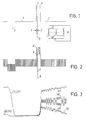
- Figure 1 shows, in correspondence to a refresh operation, the selection voltage used, the related control window and two values of the data voltage segment within the window, while, in respect of a cell controlled therewith and in the same time scale,
- Figure 2 shows two variations of the difference voltage at the ends of the cell and
- Figure 3 shows the optical transmission in four different operation conditions.
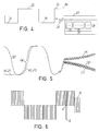
- Figure 4 shows, in correspondence to a refresh operation, the selection voltage used, the related control window and two cases of the data voltage segment within the window, while, in respect of a cell controlled therewith and in the same time scale,
- Figure 5 shows the optical transmission in three different operation conditions and
- Figure 6 shows, in expanded time scale, two variations of the difference voltage at the ends of the cell.
- Figure 7 shows, in correspondence to a selection operation, the selection voltage used, with a control window divided into two spaced apart sub-windows and four cases of the data voltage segment within the so assembled window, while, for a cell controlled therewith and in the same time scale, Figure 8 shows four variations of the difference voltage at the ends of the cell and Figure 9 shows the optical transmission in five different operation conditions.
- Figure 10 shows, in expanded time scale, the eight variations used for the data voltage segment within the windows
- Figure 11 shows, in correspondence to a selection operation, the selection voltage used and the related control window and Figure 12, in the same time scale, the optical transmission of a cell controlled by a selection voltage according to Figure 11 when the eight variations of the data voltage appearing in Figure 10 are used within the control window.
- FIG. 1 shows such selection voltage 1 in correspondence to a refresh operation.
- the first pulse 2 having a smaller amplitude than the following ones, performs the erasure of the previous image, thereby driving all cells of a row into the same state, for instance corresponding to black. It is separated by a pause 3 from the voltages relating to the selection operation, namely the two write pulses 4 and 6 and the call-back pulse 5 (by which the write operation is interrupted), corresponding in this example to the second half of the control window 7 associated to voltage 1.
- the inset 8 shows, in expanded time scale, for the data voltage segment in each control window, the two cases used, namely 9, corresponding to a control for staying in the state reached with the erasure operation (for instance, a state of minimum transmission or briefly a black state), for a pixel of the row to which voltage 1 is applied, and 10, corresponding to an opposite control for switching to the other state.
- the erasure operation for instance, a state of minimum transmission or briefly a black state
- Figure 2 shows, in the same time scale, the two variations A and B of the difference voltage 11 at the ends of a cell controlled by the selection voltage 1 and by two not shown data voltages, which are different only in correspondence to the control window 7 associated to the selection voltage 1.
- variation A practically corresponds to the worst case for white and variation B to the best case for black.
- Figure 3 shows, in the same time scale, the corresponding diagrams of the optical transmission in the two extreme cases: (a) for a cell to which voltage A is applied and that should change its state, and (b) for a cell to which voltage B is applied and that should not change its state. Furthermore, additional extreme cases (c) and (d) are shown corresponding to a data voltage the sign of which is inverted outside of the control window with respect to the one that generates the voltages shown in Figure 2. It is clear that, in a general case, diagrams intermediate between (a) and (c) in the white case and between (b) and (d) in the black case are obtained for the transmission, but transmissions intermediate between (a) and (d) will never be obtained.
- the (bistable) cell relaxes to one or the other of the two extreme stable states.
- the variability of the light transmitted within the refresh interval between the various cases corresponding to black or to white is much lower than the span appearing in Figure 3 and can be considered as effectively acceptable.
- An advantage of the first exemplary embodiment when the erasure results into a black state, is the reduced perception of light flashes by the observers at each selection operation.
- a first drawback is the above mentioned relatively noticeable effect of the data voltages outside of the control window on the transmission of the cell at the end of the selection pulses. It can be nearly eliminated by use of crosstalk compensated data voltages and by changes in the level of the selection voltage only within the control window and at the boundaries of the control windows associated to other selection voltages.
- the call-back pulse 5 has been anticipated by one half of its duration, while the other transitions of the selection voltage 1 and the control window 7 have been kept constant, and by utilizing, for data, signals such as shown in the inset 28 of Figure 4, in stead of the ones shown in inset 8.
- a better operation according to this invention has been achieved, maintaining the same above mentioned advantages.
- a second drawback is the restricted range of correct operation conditions, which depend on the thickness and on the temperature of the cell. It can be noticeably reduced by use of compensation pulses in the selection voltage.
- a third drawback is the defective efficacy of the erasure pulse, which results into a dependence of the obtained transmissions on the previous state of the cell.
- the use of double erasure pulses enables also this drawback to be eliminated, even if balancement conditions of the dc component of the selection voltage are maintained at each refresh operation. Thanks to the elimination of these three undesired effects on the cell transmission at the end of the selection operation, a lower amplitude of the useful control effect becomes sufficient and the use of lower selection voltages and/or of higher data voltages becomes possible.
- a second exemplary embodiment comprises the above mentioned improvements by which the use of nearly equal amplitudes for the selection voltages and for the data voltages is made possible.
- a selection voltage 20 having null average value and consisting of six pulses, as shown in Figure 4, corresponding to a refresh operation.
- the first (balance) pulse 21 and the second (erasure) pulse 22 effect the erasure of the previous image and are followed by a compensation pulse 23.
- the first write 24, call-back 25 and second write 26 pulses follow.
- the subsequent selection voltages have equal patterns, delayed by multiples of the control window duration.
- the call-back pulse 25 corresponds to the central half of the control window 25 associated to voltage 20.
- the inset 28 shows, in expanded time scale, for the data voltage segment in each control window, the two examined cases, namely case 29 corresponding to switching a pixel to the state of maximum light transmission (white) and case 30 corresponding to switching a pixel to the state of minimum light transmission (black).
- Figure 5 shows, in the same time scale, the diagrams of the optical transmission of the cell in connection with the two extreme cases, for instance corresponding to the worst white (e) and to the best black (f).
- a third diagram (g) is additionally shown, corresponding to the worst case for black, wherefrom the middle portion has been omitted in order to avoid garbling of the representation due to its overlap to (f).
- Figure 6 shows in expanded time scale the corresponding variations E (for worst white) and F (for best black) of the difference voltage 31 at the ends of a cell controlled with the selection voltage 20 and with two not shown data voltages, different only in correspondence to the control window 27 associated to the selection voltage 20.
- Transmission (g) of Figure 5 is obtained in connection with an inverted sign data voltage outside of the control window with respect to the one producing the voltage shown in Figure 6. It should be understood that, in the general case of black, diagrams intermediate between (f) and (g) are obtained for transmission, while transmissions intermediate between (e) and (g) will never be obtained.
- the third exemplary embodiment corresponds to Figures 7, 8 and 9, which show, in the same time scale, the sole selection operations for cell initially in the state corresponding to black.
- the control method of the first embodiment, applied in a first sub-window of the control window, is combined with the "fast" control method of the prior art, which is applied in a second sub-window. This enables not only higher overall control effects at the end of the selection operation, but also intermediate effects corresponding to discrepant controls within the two sub-windows to be obtained.
- the effects of data within the first sub-window appear to be much higher than those of data within the second one and the data within the two sub-windows can be associated to bits of different weights in a binary coding of the shades to be displayed in a pixel.
- a not balanced selection voltage 40 for each row, use has been made of a not balanced selection voltage 40, as shown in Figure 7. It comprises the first write pulse 41, the call-back pulse 42 and the second write pulse 43, as well as the stop pulse 44.
- the oscillations 45 at the same frequency of the data voltages, superposed to the maximum level of the pulses, have been determined so as to minimize the undesired effects of the contemporaneously present data voltage segments, outside of the control window. Furthermore, the peak values of the voltages have been kept constant, in the presence of allowable maximum voltages for the circuits generating them.
- the long duration of pulse 43 longer than the duration of corresponding pulses in other embodiments, at its end drives in any case the state of the cell to a point, clearly beyond the middle point between the two extreme states, corresponding to a state wherein the cell is again responsive at the most to application of additional voltages having null average value, according to the "fast" or “superfast” control techniques of the prior art, while pulse 44 drives again the state of the cell near to said middle point, at either sides according to the data voltages encountered.
- the control window associated to the selection voltage 40 consists of two sub-windows 46 and 47 of equal durations, spaced apart by a time interval corresponding to four times the duration of each of them.
- the second half of the first sub-window 46 corresponds to call-back pulse 42 and the second sub-window is centered around the end of the second write pulse 43 and the begin the stop pulse 44.
- the subsequent selection voltages have equal patterns, delayed by multiples of the overall duration of the control windows, which is tw ce the duration of the sub-windows.
- Inset 48 shows, in expanded time scale, the two cases used for the data voltage in each control sub-window, resulting into four combinations.
- Cases 49 and 50 correspond to driving a pixel to a state of maximum light transmission (white) and cases 51 and 52 correspond to driving a pixel to a state of minimum light transmission (black).
- the data voltage alternately consists of first and second sub-windows. Each first sub-window is followed by the second sub-window associated to a previous selection operation. In this embodiment, each first sub-window is followed by the second sub-window associated to the second previous selection operation, so that the time interval between two sub-windows associated to the same selection operation is four times the duration of each sub-window.
- Figure 8 shows, in the same time scale as in Figure 7, the four variations HL, for maximum white; HM, for subdued white: IL, for subdued black and IM, for maximum black, of the difference voltage 53 at the ends of a cell controlled by the selection voltage 40 and by not shown data voltages, which are different only in correspondence to the control window consisting of the two sub-windows 46 and 47 and associated to the selection voltage 40.
- Figure 9 shows, in the same time scale, the corresponding diagrams of the optical transmission of the cell (hl), (hm), (il) and (im). Furthermore, the end portion of a fifth diagram 54 is shown corresponding to data voltage segments, equal within the control window, and all of which having inverted sign in the other sub-windows, with respect to the case corresponding to (il) and IL.
- the overlap of such a diagram and (il) evidences the accuracy with which it has been possible to minimize the undesired control effects by the data voltages outside of the window.
- a fourth exemplary embodiment is shown in Figures 10, 11 and 12.
- the first one shows eight variations employed for the data voltage segment in each control window.
- the last two Figures show, in the same time scale, the sole selection operations for cell initially in a state corresponding to black.
- the control method of the second example has been changed in this embodiment so as to make it adapted to realise a scale of eight shades in combination of cells wherein intermediate states or mixtures of microscopic domains of different states are stable. Aiming at minimising the undesired effects of data outside of the control window, functions of the time with null average values and substantially crosstalk compensated must be chosen therefor.
- a not balanced selection voltage 60 For each row, a not balanced selection voltage 60, as shown in Figure 11, has been used. It comprises the compensation pulse 61, the first write pulse 62, the lower voltages and the shaped call-back pulse 63 and the second write pulse 64, while the corresponding control window is designated 65.
- the shape of the lower voltages and of pulse 63 in window 65 has been determined by summing said functions, in amplitudes proportional to the established weights. Aiming at obtaining equidistant shades, weights 7, 5, 3 and 1 have been chosen for functions N, O, P and Q, respectively.
- Figure 12 shows, in the same time scale, the corresponding diagrams of the optical transmission of cell (n), (o), (p), (q), (-q), (-p), (-o) and (-n), the initial portion of some of which having been omitted to avoid garbling the figure due to overlap thereof with other ones.
- amplitudes of 40 volts have been employed for the selection voltage and amplitudes of 13 volts have been used for the data voltages.
- a row addressing time of 36 microseconds has been obtained, with an overall duration of the pulses shown in Figure 6 corresponding to 16 times the row addressing time.
- the two last examples of the control method are completed, at each refresh operation, by not shown operations wherein the dc component appearing in the illustrated portion of the selection voltage is preferably balanced and said operation can consist of a previous erasure operation or of a selection operation of the cell that initially were in the other state.
- An erasure operation can be performed as in the first or in the second example by means of single or double pulses of the selection voltage, which can be followed by a pause, immediately before the time interval shown in Figures 7, 8 and 9 or 11 and 12. Otherwise, it is possible to complete a panel refresh operation by means of selection voltages such as those shown in Figures 7 or 11, but with opposite polarities, while the data voltages are repeated with the same polarities.
Landscapes
- Engineering & Computer Science (AREA)
- Chemical & Material Sciences (AREA)
- Crystallography & Structural Chemistry (AREA)
- Physics & Mathematics (AREA)
- Computer Hardware Design (AREA)
- General Physics & Mathematics (AREA)
- Theoretical Computer Science (AREA)
- Liquid Crystal Display Device Control (AREA)
- Control Of Indicators Other Than Cathode Ray Tubes (AREA)
- Liquid Crystal (AREA)
Description
Claims (25)
- A method for controlling a matrix panel in which each picture element ideally corresponds to the intersection of an element of a first electrode set and an element of a second electrode set and materially it corresponds to an electro-optical cell comprising a ferroelectric liquid crystal in the room existing between two facing electrodes belonging to said two electrode sets, said multistable cell featuring a minimum product pulse time x pulse voltage(Amin), within the voltage range from one to eight tenths of the pulse voltage allowing the minimum pulse time(Vtmin),when spaced apart rectangular pulses having alternately opposite polarities are applied switching the cell from an extreme state to the other one, when between the pulses a high frequency voltage of constant rms amplitude(Vhf)is applied, and in which selection voltages (1) are applied to the electrodes of the first set and each of these voltages is associated, at each selection operation, to a different control time window (7), namely a time window allocated to the control by the voltage of the stable states latched by all the cells corresponding to the electrode of the first set, and in which data voltages are applied to the electrodes belonging to the second set and each of these data voltages is formed by superposing the data voltage segments for each pixel namely the voltages applied within the different control time windows (7) associated to the selection voltages and designed to control each of the cells corresponding to the electrode belonging to the second set, said voltage segments depending on each data item describing a pixel of the image to be displayed in correspondence to the electrode of the second set, in description pixel-by-pixel of the image, and wherein, upon extracting the possible voltage function of the time added to all said voltages to facilitate the implementation of the circuits generating therm, each data voltage segment has an identical average value independent of the considered electrode, of the position of the pixel and of the data item, and each selection voltage has an identical average value as the data voltages, taken as a reference value for measuring each voltage,
characterized in that the waveforms of selection voltages (1) comprise, at each selection operation, two pulses (4, 16), namely voltages having substantially always the same polarity within finite time intervals, which are of the same polarity and are spaced apart by an interruption (5), wherein voltages of opposite polarity are present, and the second of which has an absolute value of the time integral of the voltage within 0.2 Amin and 5 Amin, which is larger than the absolute value of the time integral of the voltage in the interruption,
in that the corresponding associated control time window (7) includes time intervals extending in total for at least one and no more than four fifths of the duration of said window, corresponding to the presence within the interruption of said voltages of opposite polarity,
and in that the absolute value of the time integral of said voltages of opposite polarity extended to the assembly of said time intervals is within 0.05 Amin and Amin. - A method according to claim 1, characterized in that, as concerns the first of said two pulses of the same polarity, the absolute value of the time integral of the voltage is less than 4 Amin and more than one third of the above said value for the voltages of opposite polarity within the interruption and within the control window.
- A method according to one or more of the preceding claims, characterized in that the voltages of opposite polarity within the interruption consist in no more than three half cycles of an alternate voltage.
- A method according to one or more of the preceding claims characterized in that polarity changes are present in the data voltage segment in time correspondence to the polarity changes in the selection voltages within the control windows.
- A method according to one or more of the preceding claims, characterized in that, in the selection voltages, the peak amplitude of the voltages of opposite polarity used within the interruption is between twice and one fifth of the voltage Vtmin, that is the voltage for which the cells of the panel, when they are subjected to rectangular spaced apart pulses of alternately opposite polarities and to a high frequency voltage applied within the intervals, change their states with pulses of minimum duration, and in that the peak amplitudes of the other pulses are lower than four thirds of the abovesaid peak amplitude.
- A method according to one or more of the preceding claims, characterized in that one or more pulses (23,61) are present in the selection voltage, before the write pulses and with opposite polarity, and such pulses have an absolute value of the time integral of the voltage between 0.8 Amin and 5 Amin.
- A method according to one or more of the preceding claims characterized in that further pulses or pauses (2, 3, 21, 22, 61) are present in the selection voltages.
- A method according to one or more of the preceding claims characterized in that, in each selection voltage, level changed (45) not contained in the control window are substantially centered on time instants which delimitate immediately preceding and following portions of the data voltages having null average value for any data.
- A method according to claim 8, characterized in that it holds in connection with the begin of the write pre-pulse.
- A method according to claim 9, characterized in that said write pre-pulse begins in correspondence to the begin of the control window.
- A method according to claim 8, characterized in that it holds in connection with the end of the write post-pulse.
- A method according to one or more of the preceding claims characterized in that voltages of substantially constant levels during portions of the data voltages having null average values are present in each selection voltage.
- A method according to claims 8 and 12, characterized in that, in each selection voltage, corrective terms (45) are added which produce correlations with the data voltages outside of the control window, which compensate undesired control effects.
- A method according to one or more of the preceding claims characterized in that the selection voltages within the control windows are such that their correlations with the variations employed for the data voltage segments define a scale of different correlation levels.
- A method according to one or more of the preceding claims characterized by control windows which are divided into sub-windows (46, 47), namely spaced apart time intervals, intercalated with those corresponding to the control of other electrodes of the first set.
- A method according to claim 15, characterized in that use is made of two sub-windows (46, 47) the second of which is overlapping to the end of the write post-pulse.
- A method according to one or more of the preceding claims characterized by control windows consisting of portions with corresponding different weights of the partial control effect obtained.
- A method according to one or more of the preceding claims characterized in that, besides the pulses, a high frequency voltage having a constant rms amplitude is present in the selection voltages.
- A method according to one or more of the preceding claims characterized in that the differences between the data voltage segments and any voltages present besides the pulses within the selection voltages have a substantially constant rms amplitude.
- A method according to the preceding claim characterized in that a high frequency stabilisation of the cells is carried out.
- A method according to one or more of the preceding claims characterized in that the rms amplitude of the data voltages is between one tenth and four thirds of the peak amplitude of the selection voltages.
- A method according to claims 3, 4, 14 and 19, characterized in that the data voltage segments consist of three consecutive pulses of opposite polarity, wherein, when the time integral of the voltage of the first pulse increases, the time integral of the voltage of the last pulse decreases or vice versa, being it possible to reduce the number of such pulses to two in particular variations, in which the extreme pulses vanish.
- A method according to one or more of the preceding claims characterized in that the data voltage segments are such that the time integral of the voltage from the begin of the corresponding control time window to a generic time instant therein is a function of the time wherein the average value in the control window is less than one tenth of the peak value.
- A method according to claims 3, 4, 14 and 19, characterized in that the data voltage segments consist of four consecutive pulses of opposite polarity, in variations of which the condition mentioned in claim 23 is fulfilled and, when the time integrals of the voltages of the first and of the second pulse are increased, the time integrals of the voltages of the third and of the fourth pulses are decreased or vice versa, being it possible to reduce the number of such pulses to three in particular variations, in which the extreme pulses vanish.
- A method according to one or more of the preceding claims characterized in that, in said selection voltages, stop pulses (44) can be contained, the polarities can be inverted in consecutive selection operations and the control window can be preceded by erasure pulses (2, 22), possibly preceded by dc balance pulses (21) and/or followed by a pause (3), the duration of which is less than one half minimum time between two refresh operations.
Applications Claiming Priority (3)
| Application Number | Priority Date | Filing Date | Title |
|---|---|---|---|
| ITRM940102A IT1271866B (en) | 1994-02-25 | 1994-02-25 | METHOD OF CONTROL OF A FERROELECTRIC LIQUID CRYSTAL MATERIAL PANEL. |
| ITRM940102 | 1994-02-25 | ||
| PCT/IT1995/000029 WO1995023402A1 (en) | 1994-02-25 | 1995-02-22 | A control method for a ferroelectric liquid crystal matrix panel |
Publications (2)
| Publication Number | Publication Date |
|---|---|
| EP0746839A1 EP0746839A1 (en) | 1996-12-11 |
| EP0746839B1 true EP0746839B1 (en) | 2001-10-24 |
Family
ID=11402289
Family Applications (1)
| Application Number | Title | Priority Date | Filing Date |
|---|---|---|---|
| EP95909948A Expired - Lifetime EP0746839B1 (en) | 1994-02-25 | 1995-02-22 | A control method for a ferroelectric liquid crystal matrix panel |
Country Status (7)
| Country | Link |
|---|---|
| US (1) | US6052106A (en) |
| EP (1) | EP0746839B1 (en) |
| CN (1) | CN1141683A (en) |
| AU (1) | AU1822995A (en) |
| DE (1) | DE69523444T2 (en) |
| IT (1) | IT1271866B (en) |
| WO (1) | WO1995023402A1 (en) |
Families Citing this family (8)
| Publication number | Priority date | Publication date | Assignee | Title |
|---|---|---|---|---|
| US7193625B2 (en) | 1999-04-30 | 2007-03-20 | E Ink Corporation | Methods for driving electro-optic displays, and apparatus for use therein |
| KR100542619B1 (en) * | 1997-06-20 | 2006-01-11 | 시티즌 워치 콤파니, 리미티드 | Antiferroelectric liquid crystal display and its driving method |
| US20130063333A1 (en) | 2002-10-16 | 2013-03-14 | E Ink Corporation | Electrophoretic displays |
| US11250794B2 (en) | 2004-07-27 | 2022-02-15 | E Ink Corporation | Methods for driving electrophoretic displays using dielectrophoretic forces |
| US7813169B2 (en) * | 2008-01-18 | 2010-10-12 | Qimonda Flash Gmbh | Integrated circuit and method to operate an integrated circuit |
| US20130100109A1 (en) * | 2011-10-21 | 2013-04-25 | Qualcomm Mems Technologies, Inc. | Method and device for reducing effect of polarity inversion in driving display |
| CN103530096B (en) * | 2012-07-03 | 2018-11-16 | 索尼公司 | Long-range control method, remote control equipment and display equipment |
| CN117316337B (en) * | 2023-09-04 | 2024-03-29 | 中国人民解放军国防科技大学 | Numerical simulation method and device applied to defect structures in liquid crystal systems |
Family Cites Families (3)
| Publication number | Priority date | Publication date | Assignee | Title |
|---|---|---|---|---|
| US5095377A (en) * | 1990-08-02 | 1992-03-10 | Matsushita Electric Industrial Co., Ltd. | Method of driving a ferroelectric liquid crystal matrix panel |
| JP3753440B2 (en) * | 1992-05-07 | 2006-03-08 | セイコーエプソン株式会社 | Liquid crystal display device and driving method of liquid crystal display device |
| JP3489169B2 (en) * | 1993-02-25 | 2004-01-19 | セイコーエプソン株式会社 | Driving method of liquid crystal display device |
-
1994
- 1994-02-25 IT ITRM940102A patent/IT1271866B/en active IP Right Grant
-
1995
- 1995-02-22 US US08/693,315 patent/US6052106A/en not_active Expired - Lifetime
- 1995-02-22 CN CN95191771A patent/CN1141683A/en active Pending
- 1995-02-22 DE DE69523444T patent/DE69523444T2/en not_active Expired - Lifetime
- 1995-02-22 WO PCT/IT1995/000029 patent/WO1995023402A1/en not_active Ceased
- 1995-02-22 EP EP95909948A patent/EP0746839B1/en not_active Expired - Lifetime
- 1995-02-22 AU AU18229/95A patent/AU1822995A/en not_active Abandoned
Also Published As
| Publication number | Publication date |
|---|---|
| ITRM940102A1 (en) | 1995-08-25 |
| US6052106A (en) | 2000-04-18 |
| EP0746839A1 (en) | 1996-12-11 |
| IT1271866B (en) | 1997-06-09 |
| DE69523444T2 (en) | 2002-06-27 |
| CN1141683A (en) | 1997-01-29 |
| DE69523444D1 (en) | 2001-11-29 |
| ITRM940102A0 (en) | 1994-02-25 |
| AU1822995A (en) | 1995-09-11 |
| WO1995023402A1 (en) | 1995-08-31 |
Similar Documents
| Publication | Publication Date | Title |
|---|---|---|
| US5691740A (en) | Liquid crystal apparatus and driving method | |
| US4770502A (en) | Ferroelectric liquid crystal matrix driving apparatus and method | |
| US5448383A (en) | Method of driving ferroelectric liquid crystal optical modulation device | |
| US6204835B1 (en) | Cumulative two phase drive scheme for bistable cholesteric reflective displays | |
| US5900852A (en) | Liquid crystal display device having two metastable states and driving method therefor | |
| US5092665A (en) | Driving method for ferroelectric liquid crystal optical modulation device using an auxiliary signal to prevent inversion | |
| US6567065B1 (en) | Ferroelectric liquid crystal display and method of driving the same | |
| US6052106A (en) | Control method for a ferroelectric liquid crystal matrix panel | |
| US5886678A (en) | Driving method for liquid crystal device | |
| JPH0968696A (en) | Driving method of liquid crystal element and liquid crystal device using the driving method | |
| US6351256B1 (en) | Addressing method and apparatus | |
| US6388650B1 (en) | Low voltage control method for a ferroelectric liquid crystal matrix display panel | |
| US5973657A (en) | Liquid crystal display apparatus | |
| Maltese et al. | Addressing cycles for fast settling grey shades in ferroelectric liquid crystal matrices | |
| JP3171713B2 (en) | Antiferroelectric liquid crystal display | |
| US5841419A (en) | Control method for ferroelectric liquid crystal matrix display | |
| JP3302752B2 (en) | Driving method of antiferroelectric liquid crystal panel | |
| JPH05303076A (en) | Liquid crystal device | |
| EP0698264B1 (en) | Addressing ferroelectric liquid crystal displays | |
| JP2637517B2 (en) | Liquid crystal device | |
| JP2584767B2 (en) | Driving method of liquid crystal device | |
| JP2584752B2 (en) | Liquid crystal device | |
| JPS62273513A (en) | Driving method for liquid-crystal electrooptic element | |
| US5757350A (en) | Driving method for optical modulation device | |
| CA1258327A (en) | Driving method for optical modulation device |
Legal Events
| Date | Code | Title | Description |
|---|---|---|---|
| PUAI | Public reference made under article 153(3) epc to a published international application that has entered the european phase |
Free format text: ORIGINAL CODE: 0009012 |
|
| 17P | Request for examination filed |
Effective date: 19960720 |
|
| AK | Designated contracting states |
Kind code of ref document: A1 Designated state(s): DE ES FR GB |
|
| 17Q | First examination report despatched |
Effective date: 19990115 |
|
| GRAG | Despatch of communication of intention to grant |
Free format text: ORIGINAL CODE: EPIDOS AGRA |
|
| GRAG | Despatch of communication of intention to grant |
Free format text: ORIGINAL CODE: EPIDOS AGRA |
|
| GRAH | Despatch of communication of intention to grant a patent |
Free format text: ORIGINAL CODE: EPIDOS IGRA |
|
| GRAH | Despatch of communication of intention to grant a patent |
Free format text: ORIGINAL CODE: EPIDOS IGRA |
|
| GRAA | (expected) grant |
Free format text: ORIGINAL CODE: 0009210 |
|
| AK | Designated contracting states |
Kind code of ref document: B1 Designated state(s): DE ES FR GB |
|
| REF | Corresponds to: |
Ref document number: 69523444 Country of ref document: DE Date of ref document: 20011129 |
|
| REG | Reference to a national code |
Ref country code: GB Ref legal event code: IF02 |
|
| PG25 | Lapsed in a contracting state [announced via postgrant information from national office to epo] |
Ref country code: GB Free format text: LAPSE BECAUSE OF NON-PAYMENT OF DUE FEES Effective date: 20020222 |
|
| ET | Fr: translation filed | ||
| PG25 | Lapsed in a contracting state [announced via postgrant information from national office to epo] |
Ref country code: ES Free format text: LAPSE BECAUSE OF FAILURE TO SUBMIT A TRANSLATION OF THE DESCRIPTION OR TO PAY THE FEE WITHIN THE PRESCRIBED TIME-LIMIT Effective date: 20020430 |
|
| PLBE | No opposition filed within time limit |
Free format text: ORIGINAL CODE: 0009261 |
|
| STAA | Information on the status of an ep patent application or granted ep patent |
Free format text: STATUS: NO OPPOSITION FILED WITHIN TIME LIMIT |
|
| GBPC | Gb: european patent ceased through non-payment of renewal fee |
Effective date: 20020222 |
|
| 26N | No opposition filed | ||
| PGFP | Annual fee paid to national office [announced via postgrant information from national office to epo] |
Ref country code: FR Payment date: 20120203 Year of fee payment: 18 |
|
| PGFP | Annual fee paid to national office [announced via postgrant information from national office to epo] |
Ref country code: DE Payment date: 20120229 Year of fee payment: 18 |
|
| REG | Reference to a national code |
Ref country code: FR Ref legal event code: ST Effective date: 20131031 |
|
| REG | Reference to a national code |
Ref country code: DE Ref legal event code: R119 Ref document number: 69523444 Country of ref document: DE Effective date: 20130903 |
|
| PG25 | Lapsed in a contracting state [announced via postgrant information from national office to epo] |
Ref country code: FR Free format text: LAPSE BECAUSE OF NON-PAYMENT OF DUE FEES Effective date: 20130228 Ref country code: DE Free format text: LAPSE BECAUSE OF NON-PAYMENT OF DUE FEES Effective date: 20130903 |