EP0746796B1 - Cathode for plasma addressed liquid crystal display - Google Patents
Cathode for plasma addressed liquid crystal display Download PDFInfo
- Publication number
- EP0746796B1 EP0746796B1 EP95936724A EP95936724A EP0746796B1 EP 0746796 B1 EP0746796 B1 EP 0746796B1 EP 95936724 A EP95936724 A EP 95936724A EP 95936724 A EP95936724 A EP 95936724A EP 0746796 B1 EP0746796 B1 EP 0746796B1
- Authority
- EP
- European Patent Office
- Prior art keywords
- plasma
- electrodes
- cathode
- electro
- electron affinity
- Prior art date
- Legal status (The legal status is an assumption and is not a legal conclusion. Google has not performed a legal analysis and makes no representation as to the accuracy of the status listed.)
- Expired - Lifetime
Links
- 239000004973 liquid crystal related substance Substances 0.000 title description 20
- 239000000463 material Substances 0.000 claims description 30
- 239000010432 diamond Substances 0.000 claims description 20
- 229910003460 diamond Inorganic materials 0.000 claims description 19
- OKTJSMMVPCPJKN-UHFFFAOYSA-N Carbon Chemical compound [C] OKTJSMMVPCPJKN-UHFFFAOYSA-N 0.000 claims description 8
- 229910052799 carbon Inorganic materials 0.000 claims description 6
- 239000000382 optic material Substances 0.000 claims description 6
- 230000003213 activating effect Effects 0.000 claims description 2
- PMHQVHHXPFUNSP-UHFFFAOYSA-M copper(1+);methylsulfanylmethane;bromide Chemical compound Br[Cu].CSC PMHQVHHXPFUNSP-UHFFFAOYSA-M 0.000 claims description 2
- 239000010408 film Substances 0.000 description 20
- YCLAMANSVUJYPT-UHFFFAOYSA-L aluminum chloride hydroxide hydrate Chemical compound O.[OH-].[Al+3].[Cl-] YCLAMANSVUJYPT-UHFFFAOYSA-L 0.000 description 19
- 239000007789 gas Substances 0.000 description 13
- 239000000758 substrate Substances 0.000 description 10
- 238000004544 sputter deposition Methods 0.000 description 6
- 239000010409 thin film Substances 0.000 description 6
- 238000000034 method Methods 0.000 description 5
- 239000000203 mixture Substances 0.000 description 5
- 239000010949 copper Substances 0.000 description 3
- 229910025794 LaB6 Inorganic materials 0.000 description 2
- 230000008901 benefit Effects 0.000 description 2
- 230000015572 biosynthetic process Effects 0.000 description 2
- 230000008859 change Effects 0.000 description 2
- 239000004020 conductor Substances 0.000 description 2
- 238000010276 construction Methods 0.000 description 2
- 230000000593 degrading effect Effects 0.000 description 2
- 238000000151 deposition Methods 0.000 description 2
- 230000000694 effects Effects 0.000 description 2
- 230000005684 electric field Effects 0.000 description 2
- 239000011521 glass Substances 0.000 description 2
- 229910002804 graphite Inorganic materials 0.000 description 2
- 239000010439 graphite Substances 0.000 description 2
- 239000001307 helium Substances 0.000 description 2
- 229910052734 helium Inorganic materials 0.000 description 2
- SWQJXJOGLNCZEY-UHFFFAOYSA-N helium atom Chemical compound [He] SWQJXJOGLNCZEY-UHFFFAOYSA-N 0.000 description 2
- 239000012535 impurity Substances 0.000 description 2
- 238000004519 manufacturing process Methods 0.000 description 2
- 230000004048 modification Effects 0.000 description 2
- 238000012986 modification Methods 0.000 description 2
- 230000009467 reduction Effects 0.000 description 2
- RYGMFSIKBFXOCR-UHFFFAOYSA-N Copper Chemical compound [Cu] RYGMFSIKBFXOCR-UHFFFAOYSA-N 0.000 description 1
- 241000769223 Thenea Species 0.000 description 1
- XAGFODPZIPBFFR-UHFFFAOYSA-N aluminium Chemical compound [Al] XAGFODPZIPBFFR-UHFFFAOYSA-N 0.000 description 1
- 229910052782 aluminium Inorganic materials 0.000 description 1
- 229910052785 arsenic Inorganic materials 0.000 description 1
- 230000009286 beneficial effect Effects 0.000 description 1
- 125000004432 carbon atom Chemical group C* 0.000 description 1
- 230000015556 catabolic process Effects 0.000 description 1
- 238000000576 coating method Methods 0.000 description 1
- 239000002772 conduction electron Substances 0.000 description 1
- 229910052802 copper Inorganic materials 0.000 description 1
- 210000002858 crystal cell Anatomy 0.000 description 1
- 238000013500 data storage Methods 0.000 description 1
- 238000006731 degradation reaction Methods 0.000 description 1
- 238000002242 deionisation method Methods 0.000 description 1
- 230000008021 deposition Effects 0.000 description 1
- 238000010586 diagram Methods 0.000 description 1
- 239000003989 dielectric material Substances 0.000 description 1
- 239000007772 electrode material Substances 0.000 description 1
- 238000005516 engineering process Methods 0.000 description 1
- 230000001747 exhibiting effect Effects 0.000 description 1
- AMGQUBHHOARCQH-UHFFFAOYSA-N indium;oxotin Chemical class [In].[Sn]=O AMGQUBHHOARCQH-UHFFFAOYSA-N 0.000 description 1
- 239000012212 insulator Substances 0.000 description 1
- 238000010849 ion bombardment Methods 0.000 description 1
- 238000005468 ion implantation Methods 0.000 description 1
- 150000002500 ions Chemical class 0.000 description 1
- CPLXHLVBOLITMK-UHFFFAOYSA-N magnesium oxide Inorganic materials [Mg]=O CPLXHLVBOLITMK-UHFFFAOYSA-N 0.000 description 1
- 239000000395 magnesium oxide Substances 0.000 description 1
- AXZKOIWUVFPNLO-UHFFFAOYSA-N magnesium;oxygen(2-) Chemical compound [O-2].[Mg+2] AXZKOIWUVFPNLO-UHFFFAOYSA-N 0.000 description 1
- 238000012423 maintenance Methods 0.000 description 1
- 239000011159 matrix material Substances 0.000 description 1
- 229910052757 nitrogen Inorganic materials 0.000 description 1
- 229910052698 phosphorus Inorganic materials 0.000 description 1
- 230000010287 polarization Effects 0.000 description 1
- 230000008569 process Effects 0.000 description 1
- 230000001902 propagating effect Effects 0.000 description 1
- 230000004044 response Effects 0.000 description 1
- 239000004065 semiconductor Substances 0.000 description 1
- WFKWXMTUELFFGS-UHFFFAOYSA-N tungsten Chemical compound [W] WFKWXMTUELFFGS-UHFFFAOYSA-N 0.000 description 1
- 229910052721 tungsten Inorganic materials 0.000 description 1
- 239000010937 tungsten Substances 0.000 description 1
Images

Classifications
-
- G—PHYSICS
- G02—OPTICS
- G02F—OPTICAL DEVICES OR ARRANGEMENTS FOR THE CONTROL OF LIGHT BY MODIFICATION OF THE OPTICAL PROPERTIES OF THE MEDIA OF THE ELEMENTS INVOLVED THEREIN; NON-LINEAR OPTICS; FREQUENCY-CHANGING OF LIGHT; OPTICAL LOGIC ELEMENTS; OPTICAL ANALOGUE/DIGITAL CONVERTERS
- G02F1/00—Devices or arrangements for the control of the intensity, colour, phase, polarisation or direction of light arriving from an independent light source, e.g. switching, gating or modulating; Non-linear optics
- G02F1/01—Devices or arrangements for the control of the intensity, colour, phase, polarisation or direction of light arriving from an independent light source, e.g. switching, gating or modulating; Non-linear optics for the control of the intensity, phase, polarisation or colour
- G02F1/13—Devices or arrangements for the control of the intensity, colour, phase, polarisation or direction of light arriving from an independent light source, e.g. switching, gating or modulating; Non-linear optics for the control of the intensity, phase, polarisation or colour based on liquid crystals, e.g. single liquid crystal display cells
- G02F1/133—Constructional arrangements; Operation of liquid crystal cells; Circuit arrangements
- G02F1/1333—Constructional arrangements; Manufacturing methods
- G02F1/1343—Electrodes
-
- H—ELECTRICITY
- H01—ELECTRIC ELEMENTS
- H01J—ELECTRIC DISCHARGE TUBES OR DISCHARGE LAMPS
- H01J17/00—Gas-filled discharge tubes with solid cathode
- H01J17/38—Cold-cathode tubes
- H01J17/48—Cold-cathode tubes with more than one cathode or anode, e.g. sequence-discharge tube, counting tube, dekatron
- H01J17/485—Plasma addressed liquid crystal displays [PALC]
-
- G—PHYSICS
- G02—OPTICS
- G02F—OPTICAL DEVICES OR ARRANGEMENTS FOR THE CONTROL OF LIGHT BY MODIFICATION OF THE OPTICAL PROPERTIES OF THE MEDIA OF THE ELEMENTS INVOLVED THEREIN; NON-LINEAR OPTICS; FREQUENCY-CHANGING OF LIGHT; OPTICAL LOGIC ELEMENTS; OPTICAL ANALOGUE/DIGITAL CONVERTERS
- G02F1/00—Devices or arrangements for the control of the intensity, colour, phase, polarisation or direction of light arriving from an independent light source, e.g. switching, gating or modulating; Non-linear optics
- G02F1/01—Devices or arrangements for the control of the intensity, colour, phase, polarisation or direction of light arriving from an independent light source, e.g. switching, gating or modulating; Non-linear optics for the control of the intensity, phase, polarisation or colour
- G02F1/13—Devices or arrangements for the control of the intensity, colour, phase, polarisation or direction of light arriving from an independent light source, e.g. switching, gating or modulating; Non-linear optics for the control of the intensity, phase, polarisation or colour based on liquid crystals, e.g. single liquid crystal display cells
- G02F1/133—Constructional arrangements; Operation of liquid crystal cells; Circuit arrangements
- G02F1/1333—Constructional arrangements; Manufacturing methods
- G02F1/13334—Plasma addressed liquid crystal cells [PALC]
-
- H—ELECTRICITY
- H01—ELECTRIC ELEMENTS
- H01J—ELECTRIC DISCHARGE TUBES OR DISCHARGE LAMPS
- H01J17/00—Gas-filled discharge tubes with solid cathode
- H01J17/02—Details
- H01J17/04—Electrodes; Screens
- H01J17/06—Cathodes
- H01J17/066—Cold cathodes
Definitions
- This invention relates to plasma-addressed electro-optic display panels commonly referred to as "PALC” display devices.
- These devices comprise, typically, a sandwich of: a first substrate having deposited on it parallel transparent column electrodes, commonly referred to as "ITO” columns or electrodes since indium-tin oxides are typically used, on which is deposited a colour filter layer; a second substrate comprising parallel sealed plasma channels corresponding to rows of the display crossing all of the ITO columns each of which is filled with a low pressure ionizable gas, such as helium, and containing spaced cathode and anode electrodes along the channel for ionizing the gas to create a plasma, which channels are closed off by a thin transparent insulator; and an electro-optic material, such as a liquid crystal (LC) material, located between the substrates.
- LC liquid crystal
- the structure behaves like an active matrix liquid crystal display in which the thin film transistor switches at each pixel are replaced by a plasma channel acting as a row switch and capable of selectively addressing a row of LC pixel elements.
- a plasma channel acting as a row switch and capable of selectively addressing a row of LC pixel elements.
- successive lines of data signals representing an image to be displayed are sampled at column positions and the sampled data voltages are respectively applied to the ITO columns. All but one of the row plasma channels are in the de-ionized or non-conducting state.
- the plasma of the one ionized selected channel is conducting and, in effect, establishes a reference potential on the adjacent side of a row of pixels of the LC layer, causing each LC pixel to charge up to the applied column potential of the data signal.
- the ionized channel is turned off, isolating the LC pixel charge and storing the data voltage for a frame period.
- the next row of data appears on the ITO columns, only the succeeding plasma channel row is ionized to store the data voltages in the succeeding row of LC pixels, and so on.
- the attenuation of each LC pixel to backlight or incident light is a function of the stored voltage across the pixel. A more detailed description is unnecessary because the construction, fabrication, and operation of such PALC devices can be found in Buzak et al., "A 16-Inch Full Colour Plasma Addressed Liquid Crystal Display", Digest of Tech. Papers, 1993 SID Int. Symp., Soc. for Info. Displ. pp. 883-886.
- the ideal plasma channel would allow the plasma to be established over the entire length of the channel in a short time (plasma formation time) and at low voltages. At the same time, the ideal channel would allow the plasma to be maintained for a certain time, after the ionizing voltage has been switched off, in a sufficiently conductive state so as to allow time for the pixel capacitance to charge up to the data signal voltage to be acquired by the liquid crystal pixel (data setup and capture time). After this time, the plasma must become non-conducting after a certain time (plasma decay time), so that the pixel voltage does not change after the data line is switched off.
- the ideal case would require the plasma to be established over the length of the channel and remain in enough of a conducting state to allow the data to be written on the LC pixels in less than one-half the maximum available row address time. After that the plasma must become non-conducting. This allows the rest of the line time to be used for available crosstalk reduction techniques.
- the present state of the art uses Cr/Cu/Cr electrodes coated with a layer of LaB 6 or GdB 6 .
- the present gas fill uses pure helium as the plasma gas.
- the plasma can be switched on within 3 ⁇ s by applying 350V between the anode and the cathode electrodes within the plasma channel.
- the plasma remains in a conductive state much longer (18 ⁇ s) than is required. This results in degradation of the signal on the LC pixel and does not allow time for the use of crosstalk reduction techniques.
- This can be improved by using gas mixtures that have more suitable decay times such as He-Ne.
- the electrode sputtering during the plasma state worsens with this and other gas mixtures and the lifetime of the display panel degrades.
- EP-A-545,569 and EP-A-628,944 describe PALC devices whose cathode electrodes are coated with a dielectric material which may be magnesium oxide.
- US-A-5,141,460 does not relate to PALC display devices, but relates to electron emission. It describes the use of carbon ion implantation for diamond formation on the surface of selectively shaped electrodes.
- An object of the invention is an improved PALC display device.
- a further object of the invention is a PALC display device having improved performance, reliability and lifetime.
- Another object of the invention is a PALC display device exhibiting reduced ignition voltage and having electrodes more resistant to sputtering.
- a PALC display devices comprises in the plasma channel at least on the cathode electrode a surface of a negative electron affinity (NEA) material, which means that the conduction energy band in the surface material is sufficiently close to the vacuum energy level, within 5 kT of energy, that it allows the surface to emit electrons at relatively low electric fields.
- NAA negative electron affinity
- the plasma cathode electrode comprises a conductive substrate coated with a thin film of a hard refractory NEA material that is sufficiently conductive to support electron emission.
- a preferred refractory NEA material is diamond or diamond-like carbon (DLC).
- Fig. 1 shows a flat panel display system 10, which represents a typical PALC display device and the operating electronic circuitry.
- the flat panel display system comprises a display panel 12 having a display surface 14 that contains a pattern formed by a rectangular planar array of nominally identical data storage or display elements 16 mutually spaced apart by predetermined distances in the vertical and horizontal directions.
- Each display element 16 in the array represents the overlapping portions of thin, narrow electrodes 18 arranged in vertical columns and elongate, narrow channels 20 arranged in horizontal rows.
- the electrodes 18 are hereinafter referred to from time to time as "column electrodes").
- the display elements 16 in each of the rows of channels 20 represent one line of data.
- column electrodes 18 and channels 20 determine the dimensions of display elements 16, which are typically of rectangular shape.
- Column electrodes 18 are deposited on a major surface of a first electrically nonconductive, optically transparent substrate 34, and the channel rows are usually built into a second transparent substrate 36. Skilled persons will appreciate that certain systems, such as reflective display of either the direct view or projection type, would require that only one substrate be optically transparent.
- Column electrodes 18 receive data drive signals of the analog voltage type developed on parallel output conductors 22' by different ones of output amplifiers 23 (Fig. 2) of a data driver or drive circuit 24, and channels 20 receive data strobe signals of the voltage pulse type developed on parallel output conductors 26' by different ones of output amplifiers 21 (Fig. 2) of a data strobe or strobe means or strobe circuit 28.
- Each of the channels 20 includes a reference electrode 30 (Fig. 2) to which a reference potential, such as ground, common to each channel 20 and data strobe 28 is applied.
- display system 10 employs a scan control circuit 32 that coordinates the functions of data driver 24 and data strobe 28 so that all columns of display elements 16 of display panel 12 are addressed row by row in row scan fashion.
- Display panel 12 may employ electro-optic materials of different types. For example, if it uses such material that changes the polarization state of incident light rays, display panel 12 is positioned between a pair of light polarizing filters, which cooperate with display panel 12 to change the luminance of light propagating through them. The use of a scattering liquid crystal cell as the electro-optic material would not require the use of polarizing filters, however.
- a colour filter (not shown) may be positioned within display panel 12 to develop multi-coloured images of controllable colour intensity.
- colour can also be achieved by using three separate monochrome panels 12, each of which controls one primary colour.
- Fig. 2 illustrates the PALC version of such a display panel using LC material. Only 3 of the column electrodes 18 are shown.
- the row electrodes 20 are constituted by a plurality of parallel elongated sealed channels underlying (in Fig. 2) a layer 42 of the LC material. Each of the channels 20 is filled with an ionizable gas 44, closed off with a thin dielectric sheet 45 typically of glass, and contains on an interior channel surface first and second spaced elongated electrodes 30, 31 which extend the full length of each channel.
- the first electrode 30 is grounded and is commonly called the cathode.
- the second electrode 31 is called the anode, because to it will be supplied relative to the cathode electrode a positive strobe pulse sufficient to cause electrons to be emitted from the cathode 30 to ionize the gas.
- each channel 20 has its gas ionized with a strobe pulse to form a plasma and a grounded line connection to a row of pixels in the LC layer 42 above.
- the strobe pulse terminates, and after deionization has occurred, the next channel is strobed and turned on. Since the column electrodes 18 each cross a whole column of pixels, only one plasma row connection at a time is allowed on to avoid crosstalk.
- the cathode electrode 30 is bombarded with positive ions created in the plasma, commonly called sputtering, which evaporates material from the cathode electrode and erodes the cathode to the point where ignition of the plasma or maintenance of a stable plasma is hindered.
- sputtering positive ions created in the plasma
- the commonly used Cr/Cu/Cr electrodes coated with a layer of LaB 6 or GdB 6 are subject to this sputtering problem.
- the plasma can be switched on within a sufficiently short time by applying a sufficiently high strobe pulse, after termination of the strobe pulse, the plasma remains in a conducting state much longer (18 ⁇ s) than required.
- At least the cathode electrode of a PALC display channel is provided with a surface of a NEA material.
- the NEA surface is provided on a conductive base by a thin film of a hard, refractory NEA material that has sufficient conductivity to support electron emission.
- a preferred material is a thin vapour-deposited conductive or semiconductive diamond or diamond-like carbon (DLC) film.
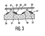
- Fig. 3 illustrates just a substrate portion of the PALC display device containing the channels 20.
- the substrate 46 typically of glass, has the channels 20 etched as described in the referenced patents and publication, and the cathode 47 and anode 48 electrodes are typically vapour deposited.
- a thin film of diamond or DLC 50 is provided over a cathode base 51 by vapour deposition. This construction will improve the switching properties of the plasma channel of the PALC display and without degrading its lifetime.
- Any electrode material which has sufficient conductivity and on which diamond or DLC thin films can be deposited can be used for the base 51. Examples are copper, aluminum and tungsten.
- Diamond and DLC films are known to possess the property of negative electron affinity (NEA), and a high density of electron emission into vacuum has been demonstrated from diamond films at low electric fields. See, for example, F.J. Himpsel et al., Phys.Rev.B,Vol. 20, No.2, July 15, 1979. pp 20 624-20 626; N. Kumar et al., IEEE Colloq. on "Diamonds In Electronics And Optics", Digest No. 1993/204, 1993, pg. 1459.
- the use of NEA films such as diamond or DLC films will have several beneficial effects on the PALC display. The ignition voltage will be lowered, so that the strobe voltages required from the drive electronics can be lowered.
- the electron emission currents will be higher, so that the plasma can be established uniformly in a short time.
- the lower voltages needed and the hardness of these diamond and DLC films will make them more resistant to sputtering than the present materials. This will not only improve the performance, but also the reliability and lifetime of the PALC display.
- the ruggedness of a diamond or DLC cathode surface will allow the use of different gas mixtures, such as He-Ne, so that the optimum gas mixture can be used without fear of degrading the lifetime or reliability of the PALC display.
- a film with a conductivity of at least 10 -4 mho/cm is preferred so that it is sufficiently electrically conductive to allow electrons to be conducted to the surface to replenish those emitted.
- Most diamond films have sufficient imperfections or inclusions, for example of graphite, which will make them sufficiently conductive to serve as cathode surfaces for establishing a plasma.
- the better quality diamond films can be doped n-type to provide the conduction electrons to the surface.
- diamond films can be made semi-conducting by doping with impurities as one would dope semiconductors, using for example impurities such as N, P or As which are co-vapour-deposited with the carbon atoms, or by using DLC films.
- DLC films naturally have graphite carbon inclusions which will provide a conduction path for electrons to the diamond crystallites which rest on the surface, as has been described in C. Wang et al., Electronics Letters, Aug. 1, 1991, Vol.27, No.16, pp.1459-1461; and N.S. Xu et al., Electronics Letters, Sept. 2, 1993, Vol.29, No.18, pp.1596-1597.
- the methods described in the above referenced publications describe in detail various ways of vapour-depositing thin films of such materials. All of the methods described will be suitable for making NEA surfaces that can serve as cathodes in an ionizable atmosphere.
- the films need not be particularly thick. Film thicknesses of at least 100 ⁇ are preferred to ensure adequate coverage of the cathode. Film thicknesses not exceeding 1 ⁇ m are preferred to ensure sufficient electron replenishment.
- the cathode electrode need be coated with the diamond or DLC film, since it is the electrode required to emit electrons and is subject to the positive ion bombardment.
- the diamond or DLC films can be coated on the anode also, without any significant loss of performance, when of reasonable conductivity. This has the advantage that it can simplify the fabrication process of the display since both electrodes can thus be coated at the same time.
- NEA materials of comparable properties can be used as coatings on top of the cathode electrode.
- One such material is AlN.
- the presence of an NEA surface has been demonstrated on AlN films grown heteroepitaxially on a conducting SiC substrates as described in M.C. Benjamin et al., Appl. Phys. Lett 64(24), June 13, 1994, pp 3288-3290.
- the channel gas filling can be the same as is used in previous PALC panels, or can be replaced by more desirable mixtures, such as He-Ne.
- the invention relates to a plasma-addressed electro-optic display device comprising a layer of electro-optic material, data electrodes coupled to the electro-optic layer and adapted to receive data voltages for activating portions of the electro-optic layer, and a plurality of plasma channels extending generally transverse to the data electrodes for selectively switching on said electro-optic portions.
- the plasma channels each comprise spaced elongated cathode and anode plasma electrodes and an ionizable gas filling.
- at least the cathode electrodes have surface portions comprised of a negative electron affinity material.
- the negative electron affinity material is a film of conductive or semiconductive diamond, diamond-like carbon, or aluminum nitride.
Landscapes
- Physics & Mathematics (AREA)
- Nonlinear Science (AREA)
- Chemical & Material Sciences (AREA)
- Crystallography & Structural Chemistry (AREA)
- Engineering & Computer Science (AREA)
- Plasma & Fusion (AREA)
- Mathematical Physics (AREA)
- General Physics & Mathematics (AREA)
- Optics & Photonics (AREA)
- Devices For Indicating Variable Information By Combining Individual Elements (AREA)
- Liquid Crystal (AREA)
- Gas-Filled Discharge Tubes (AREA)
Description
Claims (6)
- A plasma-addressed electro-optic display device (10) comprising a layer (42) of electro-optic material, data electrodes (28) coupled to the electro-optic layer and adapted to receive data voltages for activating portions of the electro-optic layer, and a plurality of plasma channels (20) extending generally transverse to the data electrodes for selectively switching on said electro-optic portions, said plasma channels each comprising spaced cathode and anode plasma electrodes (30, 31; 47, 48) and an ionizable gas filling (44), characterized in that the cathode electrodes have surface portions (50) comprised of a negative electron affinity material.
- The device of claim 1, wherein the cathode electrodes each comprise a conductive base and a film of the negative electron affinity material on the base.
- The device of claim 2, wherein the negative electron affinity material film comprises a hard refractory conductive or semiconductive material.
- The device of claim 3, wherein the negative electron affinity material film has a conductivity of at least 10-4 mho/cm.
- The device of claim 4, wherein the negative electron affinity material film has a thickness of at least 100 Å.
- The device of claim 1 or claim 4, wherein the negative electron affinity material is diamond, diamond-like carbon, or aluminum nitride.
Applications Claiming Priority (3)
| Application Number | Priority Date | Filing Date | Title |
|---|---|---|---|
| US361079 | 1994-12-21 | ||
| US08/361,079 US5705886A (en) | 1994-12-21 | 1994-12-21 | Cathode for plasma addressed liquid crystal display |
| PCT/IB1995/001074 WO1996019750A1 (en) | 1994-12-21 | 1995-11-29 | Cathode for plasma addressed liquid crystal display |
Publications (2)
| Publication Number | Publication Date |
|---|---|
| EP0746796A1 EP0746796A1 (en) | 1996-12-11 |
| EP0746796B1 true EP0746796B1 (en) | 2003-02-12 |
Family
ID=23420561
Family Applications (1)
| Application Number | Title | Priority Date | Filing Date |
|---|---|---|---|
| EP95936724A Expired - Lifetime EP0746796B1 (en) | 1994-12-21 | 1995-11-29 | Cathode for plasma addressed liquid crystal display |
Country Status (6)
| Country | Link |
|---|---|
| US (1) | US5705886A (en) |
| EP (1) | EP0746796B1 (en) |
| JP (1) | JPH09509760A (en) |
| KR (1) | KR100385498B1 (en) |
| DE (1) | DE69529608T2 (en) |
| WO (1) | WO1996019750A1 (en) |
Families Citing this family (14)
| Publication number | Priority date | Publication date | Assignee | Title |
|---|---|---|---|---|
| US5764001A (en) * | 1995-12-18 | 1998-06-09 | Philips Electronics North America Corporation | Plasma addressed liquid crystal display assembled from bonded elements |
| EP0852738A2 (en) * | 1996-07-01 | 1998-07-15 | Koninklijke Philips Electronics N.V. | A device having a plurality of channels filled with an ionizable gas |
| US5838398A (en) | 1996-09-30 | 1998-11-17 | Tektronix, Inc. | Cathode structure for a plasma addressed liquid crystal display panel |
| JP2001506800A (en) * | 1997-05-09 | 2001-05-22 | コーニンクレッカ フィリップス エレクトロニクス エヌ ヴィ | Display device |
| TW383123U (en) * | 1997-07-18 | 2000-02-21 | Koninkl Philips Electronics Nv | Display device |
| DE69804594T2 (en) * | 1997-12-19 | 2002-10-24 | Koninklijke Philips Electronics N.V., Eindhoven | DISPLAY DEVICE |
| US6236440B1 (en) * | 1998-07-22 | 2001-05-22 | U.S. Philips Corporation | Display device in which one of the two electrodes of a pixel is coated with a dipole material to equalize the electrode work functions |
| KR100292469B1 (en) * | 1998-09-14 | 2001-07-12 | 구자홍 | Lower substrate of plasma display panel and its manufacturing method |
| GB0011080D0 (en) * | 2000-05-08 | 2000-06-28 | Wang Wang N | Electrodes and plasma generating devices including electrodes |
| US6614410B2 (en) * | 2000-05-12 | 2003-09-02 | Tektronix, Inc. | Method of operating a plasma addressed liquid crystal display device to reduce sputtering |
| DE10023341A1 (en) * | 2000-05-12 | 2001-11-29 | Philips Corp Intellectual Pty | Plasma screen with protective layer |
| US6479945B2 (en) * | 2000-08-09 | 2002-11-12 | Tektronix, Inc. | Plasma addressed liquid crystal display device |
| US6897564B2 (en) * | 2002-01-14 | 2005-05-24 | Plasmion Displays, Llc. | Plasma display panel having trench discharge cells with one or more electrodes formed therein and extended to outside of the trench |
| JP5207026B2 (en) | 2007-11-30 | 2013-06-12 | トヨタ自動車株式会社 | Battery electrode current collector and battery electrode manufacturing method including the electrode current collector |
Family Cites Families (12)
| Publication number | Priority date | Publication date | Assignee | Title |
|---|---|---|---|---|
| JPS6489242A (en) * | 1987-09-30 | 1989-04-03 | Mitsubishi Electric Corp | Electrode for discharge light source |
| US5077553A (en) * | 1988-01-19 | 1991-12-31 | Tektronix, Inc. | Apparatus for and methods of addressing data storage elements |
| US5272472A (en) * | 1988-01-19 | 1993-12-21 | Tektronix, Inc. | Apparatus for addressing data storage elements with an ionizable gas excited by an AC energy source |
| US4896149A (en) * | 1988-01-19 | 1990-01-23 | Tektronix, Inc. | Addressing structure using ionizable gaseous medium |
| US5283501A (en) * | 1991-07-18 | 1994-02-01 | Motorola, Inc. | Electron device employing a low/negative electron affinity electron source |
| US5141460A (en) * | 1991-08-20 | 1992-08-25 | Jaskie James E | Method of making a field emission electron source employing a diamond coating |
| US5311204A (en) * | 1991-08-28 | 1994-05-10 | Tektronix, Inc. | Offset electrodes |
| US5536193A (en) * | 1991-11-07 | 1996-07-16 | Microelectronics And Computer Technology Corporation | Method of making wide band gap field emitter |
| US5276384A (en) * | 1992-08-26 | 1994-01-04 | Tektronix, Inc. | Electrode configuration for channel confinement of plasma discharge in an electrode structure using an ionizable gaseous medium |
| TW228592B (en) * | 1992-08-26 | 1994-08-21 | Tektronix Inc | |
| JP3319042B2 (en) * | 1993-05-25 | 2002-08-26 | ソニー株式会社 | Plasma address display |
| US5455489A (en) * | 1994-04-11 | 1995-10-03 | Bhargava; Rameshwar N. | Displays comprising doped nanocrystal phosphors |
-
1994
- 1994-12-21 US US08/361,079 patent/US5705886A/en not_active Expired - Fee Related
-
1995
- 1995-11-29 WO PCT/IB1995/001074 patent/WO1996019750A1/en not_active Ceased
- 1995-11-29 JP JP8519632A patent/JPH09509760A/en not_active Abandoned
- 1995-11-29 KR KR1019960704658A patent/KR100385498B1/en not_active Expired - Fee Related
- 1995-11-29 DE DE69529608T patent/DE69529608T2/en not_active Expired - Fee Related
- 1995-11-29 EP EP95936724A patent/EP0746796B1/en not_active Expired - Lifetime
Also Published As
| Publication number | Publication date |
|---|---|
| WO1996019750A1 (en) | 1996-06-27 |
| KR100385498B1 (en) | 2003-12-31 |
| JPH09509760A (en) | 1997-09-30 |
| KR970701372A (en) | 1997-03-17 |
| DE69529608T2 (en) | 2003-11-13 |
| US5705886A (en) | 1998-01-06 |
| DE69529608D1 (en) | 2003-03-20 |
| EP0746796A1 (en) | 1996-12-11 |
Similar Documents
| Publication | Publication Date | Title |
|---|---|---|
| US5705886A (en) | Cathode for plasma addressed liquid crystal display | |
| JP2663083B2 (en) | Address device | |
| US5783906A (en) | Sputter-resistant, low-work-function, conductive coatings for cathode electrodes in DC plasma addressing structure | |
| CA2104193C (en) | Bi-channel electrode configuration for an addressing structure using an ionizable gaseous medium and method of operating it | |
| US6007399A (en) | Hollow cathodes for plasma-containing display devices and method of producing same | |
| US5868811A (en) | Method of making a channel plate for a flat display device | |
| JP2552989B2 (en) | Plasma addressed liquid crystal display device | |
| EP0763228A1 (en) | Plasma addressed liquid crystal display with etched electrodes | |
| US6052160A (en) | Display device with sputter-resistant electrode layer for providing plasma discharge | |
| US5626772A (en) | Plasma addressed liquid crystal display with etched plasma channels | |
| US5835167A (en) | Plasma addressed liquid crystal display with reduced column voltages | |
| EP0746836B1 (en) | Channel configuration for plasma addressed liquid crystal display | |
| EP0827617B1 (en) | Plasma-addressed colour display | |
| JP3218430B2 (en) | Cathode for addressing structure | |
| US5939827A (en) | Non-reactive cathode for a PALC display panel using hydrogen-doped helium gas | |
| WO1998057219A1 (en) | Display device | |
| JPH1010561A (en) | Electro-optical device and address structure and method | |
| US6110562A (en) | Conductive anode for a PALC display panel using hydrogen-doped helium gas | |
| JP2003511716A (en) | Plasma address display |
Legal Events
| Date | Code | Title | Description |
|---|---|---|---|
| PUAI | Public reference made under article 153(3) epc to a published international application that has entered the european phase |
Free format text: ORIGINAL CODE: 0009012 |
|
| AK | Designated contracting states |
Kind code of ref document: A1 Designated state(s): DE FR GB NL |
|
| 17P | Request for examination filed |
Effective date: 19961227 |
|
| GRAG | Despatch of communication of intention to grant |
Free format text: ORIGINAL CODE: EPIDOS AGRA |
|
| 17Q | First examination report despatched |
Effective date: 20020312 |
|
| GRAG | Despatch of communication of intention to grant |
Free format text: ORIGINAL CODE: EPIDOS AGRA |
|
| GRAH | Despatch of communication of intention to grant a patent |
Free format text: ORIGINAL CODE: EPIDOS IGRA |
|
| GRAH | Despatch of communication of intention to grant a patent |
Free format text: ORIGINAL CODE: EPIDOS IGRA |
|
| GRAA | (expected) grant |
Free format text: ORIGINAL CODE: 0009210 |
|
| AK | Designated contracting states |
Designated state(s): DE FR GB NL |
|
| PG25 | Lapsed in a contracting state [announced via postgrant information from national office to epo] |
Ref country code: NL Free format text: LAPSE BECAUSE OF FAILURE TO SUBMIT A TRANSLATION OF THE DESCRIPTION OR TO PAY THE FEE WITHIN THE PRESCRIBED TIME-LIMIT Effective date: 20030212 |
|
| REG | Reference to a national code |
Ref country code: GB Ref legal event code: FG4D |
|
| REG | Reference to a national code |
Ref country code: GB Ref legal event code: 746 Effective date: 20030219 |
|
| REF | Corresponds to: |
Ref document number: 69529608 Country of ref document: DE Date of ref document: 20030320 Kind code of ref document: P |
|
| NLV1 | Nl: lapsed or annulled due to failure to fulfill the requirements of art. 29p and 29m of the patents act | ||
| ET | Fr: translation filed | ||
| REG | Reference to a national code |
Ref country code: FR Ref legal event code: D6 |
|
| PGFP | Annual fee paid to national office [announced via postgrant information from national office to epo] |
Ref country code: FR Payment date: 20031126 Year of fee payment: 9 |
|
| PGFP | Annual fee paid to national office [announced via postgrant information from national office to epo] |
Ref country code: GB Payment date: 20031128 Year of fee payment: 9 |
|
| PLBE | No opposition filed within time limit |
Free format text: ORIGINAL CODE: 0009261 |
|
| STAA | Information on the status of an ep patent application or granted ep patent |
Free format text: STATUS: NO OPPOSITION FILED WITHIN TIME LIMIT |
|
| PGFP | Annual fee paid to national office [announced via postgrant information from national office to epo] |
Ref country code: DE Payment date: 20040121 Year of fee payment: 9 |
|
| 26N | No opposition filed |
Effective date: 20031113 |
|
| PG25 | Lapsed in a contracting state [announced via postgrant information from national office to epo] |
Ref country code: GB Free format text: LAPSE BECAUSE OF NON-PAYMENT OF DUE FEES Effective date: 20041129 |
|
| PG25 | Lapsed in a contracting state [announced via postgrant information from national office to epo] |
Ref country code: DE Free format text: LAPSE BECAUSE OF NON-PAYMENT OF DUE FEES Effective date: 20050601 |
|
| GBPC | Gb: european patent ceased through non-payment of renewal fee |
Effective date: 20041129 |
|
| PG25 | Lapsed in a contracting state [announced via postgrant information from national office to epo] |
Ref country code: FR Free format text: LAPSE BECAUSE OF NON-PAYMENT OF DUE FEES Effective date: 20050729 |
|
| REG | Reference to a national code |
Ref country code: FR Ref legal event code: ST |