EP0744701A2 - Arithmetic unit and method for Fourier transform using a simplex arrangement of butterfly operation - Google Patents
Arithmetic unit and method for Fourier transform using a simplex arrangement of butterfly operation Download PDFInfo
- Publication number
- EP0744701A2 EP0744701A2 EP96303719A EP96303719A EP0744701A2 EP 0744701 A2 EP0744701 A2 EP 0744701A2 EP 96303719 A EP96303719 A EP 96303719A EP 96303719 A EP96303719 A EP 96303719A EP 0744701 A2 EP0744701 A2 EP 0744701A2
- Authority
- EP
- European Patent Office
- Prior art keywords
- data
- output
- input
- groups
- delay
- Prior art date
- Legal status (The legal status is an assumption and is not a legal conclusion. Google has not performed a legal analysis and makes no representation as to the accuracy of the status listed.)
- Withdrawn
Links
Images


Classifications
-
- G—PHYSICS
- G06—COMPUTING; CALCULATING OR COUNTING
- G06F—ELECTRIC DIGITAL DATA PROCESSING
- G06F17/00—Digital computing or data processing equipment or methods, specially adapted for specific functions
- G06F17/10—Complex mathematical operations
-
- G—PHYSICS
- G06—COMPUTING; CALCULATING OR COUNTING
- G06F—ELECTRIC DIGITAL DATA PROCESSING
- G06F17/00—Digital computing or data processing equipment or methods, specially adapted for specific functions
- G06F17/10—Complex mathematical operations
- G06F17/14—Fourier, Walsh or analogous domain transformations, e.g. Laplace, Hilbert, Karhunen-Loeve, transforms
- G06F17/141—Discrete Fourier transforms
- G06F17/142—Fast Fourier transforms, e.g. using a Cooley-Tukey type algorithm
Definitions
- the present invention relates to an arithmetic unit and a method for Fourier transform and, more particularly, to an arithmetic unit and a method enabling Fourier transform using a simpler arrangement of butterfly operations.
- high-speed Fourier transform has been performed by using a software means, i.e., programmed operation of a digital signal processor (DSP).
- DSP digital signal processor
- IC chips special hardware for performing arithmetic processing for high-speed Fourier transform have recently been brought to use.
- Such hardware means are arranged in such a manner that one butterfly operation circuit is repeatedly used or a plurality of butterfly operation circuits are arranged in parallel with each other.
- a memory for storing input data successively processed and a multiplying clock for performing arithmetic processing at a high speed are required.
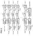
- processing data in a pipeline processing manner as shown in Fig. 11, for example, may be taken into consideration.
- input data is divided into two groups of data: one corresponding to the first half of one symbol (data supplied precedently with respect to time) and the other corresponding to the second half (data supplied by being delayed) by a distribution switch 1 of a processing circuit forming a first processing stage.
- the first-half data is supplied to a delay circuit 2 which delays data by an amount of time corresponding to N/2 (N: the number of data items (number of points) of one symbol).
- N the number of data items (number of points) of one symbol.
- the data is supplied to one (first) input of terminal (shown as an upper input terminal in Fig. 11) of a butterfly operation device 4.
- the second-half data separated by the distribution switch 1 is supplied to a multiplier 3 for the twiddle factors which performs multiplication using complex coefficients stored in a memory such as a ROM (not shown).
- a multiplier 3 for the twiddle factors which performs multiplication using complex coefficients stored in a memory such as a ROM (not shown).
- the data is supplied to the other (second) input terminal (shown as a lower input terminal in Fig. 11) of the butterfly operation device 4.
- the butterfly operation device 4 performs butterfly operation of the two inputs and outputs the result of the operation to a processing circuit forming a subsequent stage (second-stage).
- the data output from one (first) output terminal (upper output terminal in Fig. 11) of the first-stage butterfly operation device 4 is supplied to one (first) input terminal (shown as an upper input terminal in Fig. 11) of a changing switch 6-1 while the data output from the other (second) output terminal (lower output terminal in Fig. 11) of the butterfly operation device 4 is delayed by N/4 by a delay circuit 5-1 and then supplied to the other (second) input terminal (shown as a lower input terminal in Fig. 11) of the changing switch 6-1.
- the changing switch 6-1 suitably changes the data input through its two input terminals and outputs the changed data through its two output terminals.
- the data output from one (first) output terminal of the changing switch 6-1 is delayed by N/4 by a delay circuit 7-1 and then supplied to one (first) input terminal of a butterfly operation device 9-1.
- the data output from the other (second) output terminal of the changing switch 6-1 undergoes multiplication for the twiddle factors in a multiplier 8-1 for the twiddle factors and is then supplied to the other (second) input terminal of the butterfly operation device 9-1.
- the butterfly operation device 9-1 performs butterfly operation of the data input through its two input terminals and outputs the result of the operation through its two output terminals.
- Third-stage and other subsequent processing circuits have the same configuration as the second-stage processing circuit.
- the delay time of delay circuits 5-i and 7-i in the processing circuit forming each intermediate stage is 1/2 of that in the processing circuit forming the preceding stage.
- the data output from one (first) output terminal of butterfly operation device 9-k of the processing circuit forming the preceding stage is supplied directly to one (first) input terminal of a change-over switch 11 while data output from the other (second) output terminal of butterfly operation device 9-k is delayed by N/2 by a delay circuit 10A and then supplied to the other input terminal of the change-over switch 11.
- the change-over switch 11 is arranged to change the data input through the two input terminals into data in serial form and to output this data, and the output from the change-over switch 11 is rearranged by a rearrangement circuit 12.
- butterfly operation is achieved by performing both the processing of butterfly operation device 4 and the processing of the multiplier 3 for the twiddle factors in the first-stage processing circuit, for example.
- processing including no multiplication for the twiddle factors is referred to as butterfly operation (butterfly operation in a narrow sense).
- the distribution switch 1 divides each of series of data input with respect to unit symbols into first-half data (half data supplied precedently with respect to time) and second-half data (half data supplied after with respect to time).
- the distribution switch 1 supplies the first-half data to the delay circuit 2 and supplies the second-half data to the multiplier 3 for the twiddle factors.
- the delay circuit 2 delays the input first-half data by N/2 (i.e., an amount corresponding to half data of one symbol) and supplies the delayed data to one of the two input terminal of the butterfly operation device 4.
- the second-half data having being output from the distribution switch 1 and having undergone multiplication for the twiddle factors in the multiplier 3, is supplied to the other input terminal of the butterfly operation device 4.
- the multiplication time of the multiplier 3 for the twiddle factors has been ignored. If this multiplication time is not negligible, the delay time of the delay circuit 2 is set by also considering this multiplication time. Time setting is also made in the same manner with respect to the other delay circuits.).
- the delay circuit 2 the first-half data and the second half-data of the same symbol are supplied to the butterfly operation device 4 by the same timing to be input thereto simultaneously with each other (the items of each of the first-half data and second-half data being input one by one in order from the leading item).
- the butterfly operation device 4 performs radix-2 butterfly operation with respect to corresponding data items of the two groups of input data.
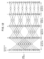
- Fig. 12 shows the principle of radix-2 butterfly operation.
- the number N of data items of one symbol is 16.
- the butterfly operation device 4 adds the first one of first-half data items represented by numbers 0 to 7, i.e., data item 0, and the first one of second-half data items represented by numbers 8 to 15, i.e., data item 8, in sixteen data items constituting a symbol g and represented by numbers 0 to 15 in Fig. 12.
- the butterfly operation device 4 also performs subtraction between the data items 0 and 8.
- the value obtained by the addition is set as data item 0 in a column p shown in Fig. 12 while the value obtained by the subtraction is set as a data item 8 in column p.
- the sum and the difference between the second one of the first-half data items of the symbol g, i.e., data item 1, and the second one of the second-half data items of the symbol g, i.e., data item 9, are calculated.
- the sum is set as data item 1 in column p while the difference is set as data item 9 in column p.
- the subsequent data items are processed in the same manner.
- sixteen data items represented by numbers 0 to 15 in column p are obtained.
- the group of eight data items in the first half of column p, represented by numbers 0 to 7, and the group of eight data items in the second half of column p, represented by numbers 8 to 15, are supplied in parallel with each other to the processing circuit forming the subsequent stage, each group of data items being sent in serial order.
- the second-stage processing circuit eight data items 0 to 7 in the first half of column p, output from the first-stage butterfly operation device 4, are supplied directly to one of the two input terminals of the changing switch 6-1 while eight data items 8 to 15 in the second half are input to the delay circuit 5-1.
- the data items input to the delay circuit 5-1 are delayed by N/4 (i.e., an amount corresponding to a quarter of the symbol) and then supplied to the other input terminal of the changing switch 6-1.
- the changing switch 6-1 executes processing for suitably changing the data items supplied to the two input terminals shown as upper and lower terminals in Fig. 11.
- first-half four data items 0 to 3 in column-p data items 0 to 7 supplied through the upper input terminal are supplied to the delay circuit 7-1.
- second-half four data items 4 to 7 in column-p data items 0 to 7 are output to the multiplier 8-1 for the twiddle factors.
- Four column-p data items 8 to 11 which are supplied to the lower input terminal of the changing switch 6-1 when four column-p data items 4 to 7 are supplied to the upper input terminal of the changing switch 6-1 are supplied to the delay circuit 7-1.
- Four column-p data items 12 to 15, input subsequently, are supplied to the multiplier 8-1 for the twiddle factors.
- data items 0 to 3 and 8 to 11 are successively output from the first output terminal of the changing switch 6-1 while data items 4 to 7 and 12 to 15 are successively output from the second output terminal.
- the delay circuit 7-1 delays four input column-p data items 0 to 3 by N/4 and supplies these data items to one of the two input terminals of the butterfly operation device 9-1. At this time, four data items 4 to 7 which have undergone multiplication for the twiddle factors in the multiplier 8-1 are supplied to the other input terminal of the butterfly operation device 9-1. That is, by virtue of the delay circuit 7-1, data items 0 to 3 and data items 4 to 7 are supplied to the butterfly operation device 9-1 by the same timing to be input thereto simultaneously with each other.
- the butterfly operation device 9-1 calculates the sum and difference between column-p data items 0 and 4, sets the sum as data item 0 in column q and sets the difference as data item 4 in column q.
- the butterfly operation device 9-1 also calculates the sum and difference between column-p data items 1 and 5, sets the sum as data item 1 in column q and sets the difference as data item 5 in column q.
- the same processing is repeated to obtain eight column-q data items 0 to 7 from column-p data items 0 to 7.
- the delay circuit 7-1 delays four subsequently-input data items 8 to 11 by N/4 and supplies these data items to the above-mentioned one input terminal of the butterfly operation device 9-1.
- four data items 12 to 15 which have undergone multiplication for the twiddle factors in the multiplier 8-1 are supplied to the other input terminal of the butterfly operation device 9-1. That is, four data items 8 to 11 and four data items 12 to 15 are supplied to the two input terminals of the butterfly operation device 9-1 by the same timing to be input thereto simultaneously with each other.
- the butterfly operation device 9-1 calculates the sum and difference between column-p data items 8 and 12, sets the sum as data item 8 in column q and sets the difference as data item 12 in column q.
- the butterfly operation device 9-1 also calculates the sum and difference between column-p data items 9 and 13, sets the sum as data item 9 in column q and sets the difference as data item 13 in column q.
- the subsequent column-p data items are processed in the same manner.
- eight column-q data items 8 to 15 are obtained from eight column-p data items 8 to 15.
- the data output from the upper output terminal of the butterfly operation device 9-k as shown in Fig. 11 is supplied to the upper input terminal of the change-over switch 11 while the data output from the lower output terminal of the butterfly operation device 9-k is delayed by N/2 by the delay circuit 10A and then supplied to the lower input terminal of the change-over switch 11.
- the change-over switch 11 first selects and outputs data items 0, 2, 4, 6, 8, 10, 12, and 14 in column G shown in Fig. 12, which are supplied to the upper input terminal.
- the change-over switch 11 next selects and outputs data items 1, 3, 5, 7, 9, 11, 13, and 15 in column G, which are input from the delay circuit 10A.
- the rearrangement circuit 12 rearrange these data items into a sequence, e.g., 0, 8, 4, 12, 2, 10, 6, 14, 1, 9, 5, 13, 3, 11, 7, 15 (by so-called bit reverse processing mentioned below in the description of an embodiment of the present invention) and outputs this sequence of data items.
- serial data input to the distribution switch 1 is successively processed in a pipeline processing manner through the processing stages by being divided into groups of data items processed in parallel with each other, and the processed data items are again changed into serial data by the change-over switch 11.
- This serial data is output at the same clock rate as the serial data input to the distribution switch 1.
- the distribution switch 1, the changing switch 6-1 to 6-k and the change-over switch 11 in the processing stages are controlled by predetermined timing by a timing control circuit (not shown).
- the number of delay circuits required in this example is 2(N - 1).
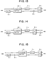
- the multiplier 8-i for the twiddle factors (multiplier 3) in each stage is inserted between the lower output terminal of the changing switch 6-i (distribution switch 1) and the lower input terminal of the butterfly operation device 9-i (butterfly operation device 4), as shown in Fig. 13.
- it may be connected to the lower output terminal of the butterfly operation device 9-i, as shown in Fig. 14.
- multiplier 8-i for the twiddle factors may alternatively be inserted between the delay circuit 5-i and the lower input terminal of the changing switch 6-i. In each case, the same operation result can be obtained as in the case of using the arrangement shown in Fig. 13. However, multiplying values of multiplication for the twiddle factors are changed according to the inserted position.
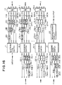
- Fig. 16 shows an example of radix-4 butterfly operation relating to radix-2 butterfly operation of the processing system shown in Fig. 11.
- a first-stage distribution switch 11 divides data of each of input symbols into quarters and outputs the divided data items.
- the first quarter of the data is delayed by N/4 by each of delay circuits 12A, 12B, and 12C, that is, delayed by 3N/4 in total and then supplied to a first input terminal of a butterfly operation device 14.
- the second quarter of the data is delayed by N/4 by each of delay circuits 12D and 12E, that is, delayed by N/2 in total and then input to a multiplier 13A for the twiddle factors.
- the multiplier 13A multiplies the input data by complex coefficients stored in a memory such as a ROM (not shown) and supplies the result of this multiplication to a second input terminal of the butterfly operation device 14.
- the third quarter of the data output from the distribution switch 11 is delayed by N/4 by a delay circuit 12F and then input to a multiplier 13B for the twiddle factors.
- the multiplier 13B performs multiplication of the input data with respect to the twiddle factors and supplies the result of this multiplication to a third input terminal of the butterfly operation device 14.
- the fourth quarter of the data output from the distribution switch 11 undergoes multiplication for the twiddle factors performed by a multiplier 13C for the twiddle factors and is then supplied to a fourth input terminal of the butterfly operation device 14.
- the butterfly operation device 14 performs butterfly operation of the groups of data input through the four input terminals and successively outputs each of the four parallel groups of data to a second-stage processing circuit.
- the data output from a first output terminal of the first-stage butterfly operation device 14 is input directly to a first input terminal of a changing switch 16-1.
- the data output from a second output terminal of the butterfly operation device 14 is delayed by N/16 by a delay circuit 15F-1 and then supplied to a second input terminal of the changing switch 16-1.
- the data output from a third output terminal of the butterfly operation device 14 is delayed by N/16 by each of delay circuits 15D-1 and 15E-1, that is, delayed by N/8 in total and then supplied to a third input terminal of the changing switch 16-1.
- the data output from a fourth output terminal of the butterfly operation device 14 is delayed by N/16 by each of delay circuits 15A-1, 15B-1, and 15C-1, that is, delayed by 3N/16 in total and then supplied to a fourth input terminal of the changing switch 16-1.
- the changing switch 16-1 suitably selects data items input through its four input terminals and outputs the selected data items through its four output terminals.
- the data output from the first output terminal of the changing switch 16-1 is delayed by N/16 by each of delay circuits 17A-1, 17B-1, and 17C-1, that is, delayed by 3N/16 in total and then supplied to a first input terminal of a butterfly operation device 19-1.
- the data output from the second output terminal of the changing switch 16-1 is delayed by N/16 by each of delay circuits 17D-1 and 17E-1, that is, delayed by N/8 in total and then input to a multiplier 18A-1 for the twiddle factors.
- the multiplier 18A-1 performs multiplication of the input data with respect to the twiddle factors and supplies the result of this multiplication to a second input terminal of the butterfly operation device 19-1.
- the data output from the third output terminal of the changing switch 16-1 is delayed by N/16 by a delay circuit 17F-1 and then input to a multiplier 18B-1 for the twiddle factors.
- the multiplier 18B-1 performs multiplication of the input data with respect to the twiddle factors and supplies the result of this multiplication to a third input terminal of the butterfly operation device 19-1.
- the data output from the fourth output terminal of the changing switch 16-1 undergoes multiplication for the twiddle factors performed by a multiplier 18C-1 for the twiddle factors and is then supplied to a fourth input terminal of the butterfly operation device 19-1.
- the delay time of the delay circuits in each stage is 1/2 of that of the delay circuits in the preceding stage. In contrast, in this example, the delay time of each stage is 1/4 of that of the preceding stage.
- the data output from each of first to fourth output terminals of a butterfly operation device 19-k in a stage in which the delay time of delay circuits corresponds to one data item is supplied to the corresponding one of first to fourth input terminals of a change-over switch 21 directly or after being delayed by N/4 by a delay circuit 20F, delay circuits 20D and 20E or delay circuits 20A to 20C.
- the change-over switch 21 suitably selects data items input through the first to fourth terminals in parallel with each other and outputs the selected data items as serial data.
- a rearrangement circuit 22 rearranges outputs from the change-over switch 11 and outputs rearranged data.
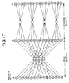
- the distribution switch 11 divides each of series of data input with respect to unit symbols into four groups and outputs the divided groups of data through the first to fourth output terminals. For example, if one symbol is constituted of 16 data items as shown in Fig. 17, four data items of symbol g represented by numbers 0 to 3 are output through the first terminal; four data items represented by numbers 4 to 7, through the second output terminal; four data items represented by numbers 8 to 11, through the third output terminal; and four data items represented by numbers 12 to 15, through the fourth output terminal.
- Four data items 0 to 3 ahead of the others with respect to time are delayed by a total of 3N/4 by the delay circuits 12A, 12B, and 12C and supplied to the first input terminal of the butterfly operation device 14.
- Four data items 4 to 7 are delayed by a total of N/2 by the delay circuits 12D and 12E, then undergo multiplication for the twiddle factors in the multiplier 13A for the twiddle factors, and are supplied to the second input terminal of the butterfly operation device 14.
- Four data items 8 to 11 are delayed by N/4 by the delay circuit 12F and then input to the multiplier 13B for the twiddle factors. These data items are supplied to the third input terminal of the butterfly operation device 14 after undergoing multiplication for the twiddle factors.
- Four data items 12 to 15 undergo multiplication for the twiddle factors in the multiplier 13C for the twiddle factors and are thereafter supplied to the fourth input terminal of the butterfly operation device 14.
- the groups of four data items are respectively supplied to the four input terminals of the butterfly operation device 14 by the same timing to be input thereto simultaneously with each other, the data items in each group being input in serial order.
- the butterfly operation device 14 performs butterfly operation of data items 0, 4, 8, and 12 respectively input from the four input terminals, as shown in Fig. 17. As the result of this operation, data items 0, 4, 8, and 12 in column p shown in Fig. 17 are set.
- butterfly operation of data items 1, 5, 9, and 13 of symbol g are performed to set data items 1, 5, 9, and 13 in column p.
- the subsequent data items of symbol g are processed in the same manner.
- sixteen data items in column p are calculated from the sixteen data items of symbol g. These operation results are output to the second-stage processing circuit.
- p-column data items 0 to 3 are supplied to the first terminal of the changing switch 16-1, and column-p data items 4 to 7 are delayed by N/16 by the delay circuit 15F-1 and then supplied to the second input terminal.
- Data items 8 to 11 are delayed by a total of N/8 by the delay circuits 15D-1 and 15E-1 and then supplied to the third input terminal.
- Data items 12 to 15 are delayed by a total of 3N/16 by the delay circuits 15A-1, 15B-1, and 15C-1 and then supplied to the fourth input terminal.
- the changing switch 16-1 first selects column-p data item 0 output from the first output terminal of the butterfly operation device 14 and input through the first input terminal of the changing switch 16-1, and outputs this data item through the first output terminal.
- Data item 0 output from the first output terminal of the changing switch 16-1 is delayed by 3N/16 by the delay circuits 17A-1, 17B-1, and 17C-1 and then supplied to the first input terminal of the butterfly operation device 19-1.
- data items 1 and 4 are respectively supplied to the first input terminal and the second input terminal of the changing switch 16-1.
- Data item 1 is output through the second output terminal while data item 4 is output through the first output terminal.
- data items 2, 5, and 8 supplied next time are output through the third, second and first output terminals, respectively;
- data items 3, 6, 9, and 12 are output through the fourth, third, second and first output terminals, respectively;
- data items 7, 10, and 13 are output through the fourth, third and second output terminals, respectively;
- data items 11 and 14 are output through the fourth and third output terminals, respectively; and
- data item 15 is output through the fourth output terminal.
- column-p data items 0 to 3 are respectively supplied to the first to fourth input terminals of the butterfly operation device 19-1 by the same timing to be input thereto simultaneously with each other.
- the butterfly operation device 19-1 performs butterfly operation of these four data items to form data items 0 to 3 in column G.
- the operation of the butterfly operation devices is completed by the above-descried processing. If the number of data items of one symbol is larger than sixteen, the same processing is performed in other one or more subsequent processing circuits.
- data item 0 is supplied to the first input terminal of the change-over switch 21 without being delayed.
- Data item 1 is delayed by N/4 by the delay circuit 20F
- data item 2 is delayed by N/2 by the delay circuit 20D and 20E
- data item 3 is delayed by 3N/4 by the delay circuits 20A, 20B, and 20C before they are respectively supplied to the second to third input terminals of the change-over switch 21.
- the change-over switch 21 selects and outputs data items 0, 4, 8, and 12 input through the first input terminal in the first period of N/4 and selects and outputs data items 1, 5, 9, and 13 input through the second input terminal in the next N/4 period. In the subsequent periods, the change-over switch 21 selects and outputs data items 2, 6, 10, and 14 input through the second input terminal and data items 3, 7, 11, and 15 input through the third input terminal.
- the data items are output in serial form and are rearranged in the order from 0 to 15 in the rearrangement circuit 22.
- the number of delay circuits is 2(N - 1). In the case of the system shown in Fig. 16, in which the radix is 4, the number of delay circuits is 4(N - 1). (If the radix is R, the number of delay circuits is R(N - 1).
- the position of the multipliers for the twiddle factors is not restricted and there is no limit to the radix of fast Fourier transform. Further, there is no restriction on setting the amount of delay.
- series of data are input to or output from each stage in parallel with each other.
- each butterfly operation device in the conventional Fourier transform arithmetic unit, a plurality of operations are performed by each butterfly operation device at a time. Accordingly, the construction of each butterfly operation device is complicated, so that the overall size of the arithmetic unit is large and the cost for manufacturing the arithmetic unit is high.
- an object of the present invention is to provide an arithmetic unit and a method which enable Fourier transform using simpler butterfly operation devices such that the size and the manufacturing cost of the arithmetic unit are reduced.
- a Fourier transform arithmetic unit comprising a plurality of processing stages for performing fast Fourier transform by pipeline processing, each of the plurality of processing stages having timing control means for dividing input data responding to one symbol into a plurality of groups of data and for outputting the plurality of divided groups of data a certain number of times by the same timing, and first operation means supplied with the plurality of groups of data output a certain number of times by the same timing by the timing control means, the first operation means performing predetermined operation each time the plurality of groups of data are input, the first operation means outputting a result of butterfly operation in a time division manner.
- a Fourier transform operation method of performing fast Fourier transform by pipeline processing using a plurality of processing stages comprising, in each of the plurality of processing stages, a first step of dividing input data corresponding to one symbol into a plurality of groups of data, a second step of outputting the plurality of divided groups of data a certain number of times by the same timing, and a third step of performing predetermined operation each time the plurality of groups of data are supplied by the same timing, and outputting a result of butterfly operation in a time division manner.
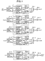
- Fig. 1 is a block diagram showing the configuration of a first embodiment of a Fourier transform arithmetic unit in accordance with the present invention.
- a distribution switch 31-1 of a processing circuit forming an initial stage divides input data into first-half data preceding with respect to time and second-half data following the first-half data.
- the first-half data is supplied to a delay circuit 32A-1 via a second input terminal of a change-over switch 36A-1.
- An output from the delay circuit 32A-1 obtained by delaying the data by N/2 (N: the number of data items of one symbol) is again input to the delay circuit 32A-1 via a first input terminal of the change-over switch 36A-1.
- the second-half data distributed by the distribution switch 31-1 is input to a delay circuit 32B-1 via a first input terminal of a change-over switch 36B-1.
- the data output from the delay circuit 32B-1 after being delayed by N/2 by this circuit is again input to the delay circuit 32B-1 via a second input terminal of the change-over switch 36B-1.
- a butterfly operation device 34-1 fetches the data output from the delay circuit 32A-1 and the data output from the change-over switch 36B-1, performs butterfly operation using these groups of data and outputs the result of this operation to a multiplier 33-1 for the twiddle factors.
- the multiplier 33-1 performs multiplication of the input data with respect to the twiddle factors and outputs the result of this multiplication to a processing circuit forming a subsequent stage.
- Processing circuits forming the second and other subsequent processing stages are arranged in the same manner as the first-stage processing circuit. However, the delay time of the delay circuits in each of the subsequent processing stages is 1/2 of that in the preceding stage.
- the distribution switch 31-1 divides input data corresponding to each of unit symbols into first-half data and second-half data (Fig. 2(A)), supplies the first-half data to the second input terminal of the change-over switch 36A-1 (Fig. 2(B)) and supplies the second-half data to the first input terminal of the change-over switch 36B-1 (Fig. 2(C)).
- the data input to the change-over switch 36A-1 through the second input terminal of this switch is supplied and written to the delay circuit 32A-1.
- first-half data f 0 of a symbol f is written to the delay circuit 32A-1.
- this data f 0 is read out from the delay circuit 32A-1 to be supplied to the first input terminal of the butterfly operation device 34-1.
- Second-half data f 1 distributed by the distribution switch 31-1 is input to the change-over switch 36B-1 through the first input terminal of this switch by the same timing as data f 0 supplied to the first input terminal of the butterfly operation device 34-1. Second-half data f 1 is thereby supplied to the second input terminal of the butterfly operation device 34-1.
- the butterfly operation device 34-1 performs one of two necessary operations, e.g., addition (f 0 + f 1 ) with respect to first-half data f 0 and second-half data f 1 simultaneously input to its two input terminals and outputs the result of this operation (Fig. 2(F)).
- first-half data f 0 read out from delay circuit 32A-1 is again written to the delay circuit 32A-1 via the first input terminal of the change-over switch 36A-1 (Fig. 2(D)).
- second-half data f 1 output from the change-over switch 36B-1 is written to the delay circuit 32B-1 (Fig. 2(E)) while the operation of this data is being performed by the butterfly operation device 34-1.
- first-half data f 0 is again output from the delay circuit 32A-1 and second-half data f 1 is read out from the delay circuit 32B-1.
- first-half data f 0 and second-half data f 1 are output through the change-over switch 36B-1.
- the same data is again input to the butterfly operation device 34-1.
- the butterfly operation device 34-1 performs the other of its operations not performed at the preceding time, e.g., subtraction (f 0 - f 1 ) of first-half data f 0 and second-half data f 1 again input and outputs the result of this operation.
- first-half data f0 When first-half data f0 is being read out from the delay circuit 32A-1, first-half data g 0 of the next symbol g is supplied from the distribution switch 31-1 and written to the delay circuit 32A-1 via the second input terminal of the change-over switch 36A-1.
- butterfly operation can be performed continually with respect to the data of input symbols.
- the result of butterfly operation performed by the butterfly operation device 34-1 is input to the multiplier 33-1 for the twiddle factors. After undergoing multiplication for the twiddle factors, the operation result is output to the processing circuit forming the subsequent stage.
- butterfly operation is performed in the butterfly operation device 34-1 in a time division manner. It is sufficient for the butterfly operation device 34-1 to perform one operation (addition or subtraction) at a time. Therefore, the scale of the circuit of the present invention can be reduced in comparison with the circuit arranged to perform two operations (both addition and subtraction) at a time.
- the number of delay circuits in this embodiment is 2(N - 1).
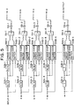
- Fig. 3 shows the configuration of another embodiment of the present invention in which radix-4 operation relating to the radix-2 operation of the embodiment of radix-2 operation shown in Fig. 1 is performed.
- a distribution switch 41A-1 divides input data into quarters and outputs the divided data through its first to fourth output terminals. It is necessary for the data output from the first output terminal of the distribution switch 41A-1 to be delayed by a total of 3N/4 before being supplied to a first input terminal of a butterfly operation device 44-1. It is necessary for the data output from the second output terminal to be delayed by N/2 before being supplied to a second input terminal of the butterfly operation device 44-1.
- the data output from the first output terminal of the distribution switch 41A-1 in a processing circuit forming an initial stage is supplied to a second input terminal of a change-over switch 46A-1 or to a second input terminal of a changeover switch 46B-1 via a first or second output terminal of a distribution switch 41B-1.
- the change-over switch 46A-1 selects one of an output from a delay circuit 42A-1 which delays data by N/4 and an output from a first output terminal of the distribution switch 41B-1, and supplies the selected data to the delay circuit 42A-1.
- the change-over switch 46B-1 selects one of an output from a delay circuit 42B-1 which delays data by N/4 and an output from a second output terminal of the distribution switch 41B-1, and outputs the selected data to the delay circuit 42B-1.
- a change-over switch 46F-1 selects one of an output from a delay circuit 42A-1 and an output from the delay circuit 42B-1 and supplies the selected data to the first input terminal of the butterfly operation device 44-1.
- a change-over switch 46C-1 selects one of the data output from the second output terminal of the distribution switch 41A-1 and an output from a delay circuit 42C-1 which delays data by N/4.
- the change-over switch 46C-1 outputs the selected data to the delay circuit 42C-1.
- a delay circuit 42E-1 delays an output from the delay circuit 42C-1 and supplies the delayed data to the second input terminal of the butterfly operation device 44-1.
- a change-over switch 46D-1 selects one of the data output from the third output terminal of the distribution switch 41A-1 and data output from a delay circuit 46D-1 which delays data by N/4.
- the change-over switch 46D-1 supplies the selected data to the delay circuit 46D-1.
- An output from the delay circuit 46D-1 is supplied to the third input terminal of the butterfly operation device 44-1.
- a change-over switch 46E-1 selects one of the data output from the fourth output terminal of the distribution switch 41A-1 and data output from a delay circuit 42F-1 which delays data by N/4.
- the change-over switch 46E-1 supplies the selected data to the delay circuit 46D-1 and to the fourth input terminal of the butterfly operation device 44-1.
- One output from the butterfly operation device 44-1 is input to a multiplier for the twiddle factors 43-1. After undergoing multiplication for the twiddle factors, the data is output to a processing circuit forming a subsequent stage.
- Processing circuits forming the second and other subsequent stages are arranged in the same manner. However, the delay time of the delay circuits in each of the subsequent processing stages is 1/4 of that in the preceding stage.
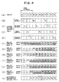
- the initial-stage distribution switch 41A-1 divides input data corresponding to each of unit symbols (Fig. 4(A)) into quarters. For example, the distribution switch 41A-1 divides a symbol f into first-quarter data f 0 , second-quarter data f 1 , third-quarter data f 2 and fourth-quarter data f 3 .
- the distribution switch 41A-1 outputs these groups of data through its first to fourth output terminals (Figs. 4(B) to 4(E)).
- the data output from the first output terminal of the distribution switch 41A-1 is input to the distribution switch 41B-1 to be supplied to the change-over switch 46A-1 or to the change-over switch 46B-1.
- the distribution switch 41B-1 distributes input data to the change-over switch 46A-1 and to the change-over switch 46B-1 alternately with respect to unit symbols. For example, if the data of symbol f is supplied to the change-over switch 46A-1, the data of the next symbol g is output to the change-over switch 46B-1. The data of the next but one symbol h is again supplied to the change-over switch 46A-1.
- data f 0 of the first symbol f is supplied to the change-over switch 46A-1.
- the change-over switch 46A-1 supplies this data to the delay circuit 42A-1 to write the data to this delay circuit (Fig. 4(F)).
- Data f 0 written to the delay circuit 42A-1 is delayed by N/4 and then read out to be again input to the same delay circuit 42A-1 through the change-over switch 46A-1.
- data f 0 is delayed by a total of 3N/4 by repeating this operation, it is supplied to the first input terminal of the butterfly operation device 44-1 through the change-over switch 46F-1.
- Second-quarter data f 1 output from the second output terminal of the distribution switch 41A-1 is input and written to the delay circuit 42C-1 through the change-over switch 46C-1 (Fig. 4(H)).
- the delay circuit 42C-1 delays the input data by N/4 and outputs the delayed data.
- This data f 1 output from the delay circuit 42C-1 is again input and written to the delay circuit 42C-1 through the change-over switch 46C-1. This operation is repeatedly performed.
- the delay circuit 42E-1 further delays by N/4 the data delayed by N/4 by the delay circuit 42C-1 and supplies the data to the second input terminal of the butterfly operation device 44-1 (Fig. 4(J)). Accordingly, data f 1 is input to the second terminal of the butterfly operation device 44-1 when data f 0 is input to the first input terminal of the butterfly operation device 44-1.
- Third-quarter data f 2 output from the third output terminal of the distribution switch 41A-1 is input and written to the delay circuit 42D-1 via the second input terminal of the change-over switch 46D-1 (Fig. 4(I)). After being delayed by N/4 by the delay circuit 42D-1, data f 2 is again input to the delay circuit 42D-1 via the first input terminal of the change-over switch 46D-1 to be delayed. This operation is repeatedly performed.
- data f 2 from the delay circuit 42D-1 is supplied to the third input terminal of the butterfly operation device 44-1 when data f 0 and data f 1 are supplied to the first and second input terminals of the butterfly operation device 44-1.
- Fourth-quarter data f 3 output from the fourth output terminal of the distribution switch 41A-1 is written to the delay circuit 42F-1 via the first input terminal of the change-over switch 46E-1 (Fig. 4(K)) and is simultaneously supplied to the fourth input terminal of the butterfly operation device 44-1.
- groups of data f 0 to f 3 as the quarters of symbol f are supplied to the first to fourth input terminals of the butterfly operation device 44-1 simultaneously with each other, data items in each group being input in serial order.
- the butterfly operation device 44-1 performs predetermined one of four butterfly operations which are to be performed with respect to the four groups of data f 0 to f 3 , and outputs operation result F 0 (Fig. 4(L)).
- Data f 0 is again supplied from the delay circuit 42A-1 to the first input terminal of the butterfly operation device 44-1 through the change-over switch 46F-1 at the time of the next input subsequent to the time when the butterfly operation device 44-1 finishes outputting the operation result F 0 (Fig. 4(F)).
- data f 1 is supplied from the delay circuit 42E-1 to the second input terminal (Fig. 4(J))
- data f 2 is supplied from the delay circuit 42D-1 to the third input terminal (Fig. 4(I))
- data f 3 is supplied from the delay circuit 42F-1 to the fourth input terminal via the change-over switch 46E-1 (Fig. 4(K)).
- the butterfly operation device 44-1 performs the second one of the four butterfly operations and outputs operation result F 1 (Fig. 4(L)).
- the first data g 0 cannot be supplied and written to the delay circuit 42A-1. That is, it is still necessary for the delay circuit 42A-1 to hold data f 0 and to supply this data to the butterfly operation device 44-1. Therefore, the distribution switch 41B-1 supplies data g 0 to the delay circuit 42B-1 through the change-over switch 46B-1, thereby writing the data to the delay circuit 42B-1 (Fig. 4(G)).
- the delay circuit 42B-1 delays the input data g 0 by N/4 and outputs the delayed data. This delayed data g 0 is again input to the delay circuit 42B-1 through the change-over switch 46B-1 to be delayed. This operation is repeatedly executed.
- the data output from the butterfly operation device 44-1 is input to the multiplier 43-1 for the twiddle factors. After undergoing multiplication for twiddle factors, the data is output to the processing circuit forming the subsequent stage.
- Processing similar to that of the first-stage processing circuit is performed in each of the second-stage and other subsequent processing circuits.
- the number of delay circuits in this embodiment is 2(N - 1).
- Fig. 5 shows a third embodiment of the present invention in which radix-2 fast Fourier transform is performed.
- no distribution switch corresponding to the distribution switch 31-1 of the embodiment shown in Fig. 1 is used and input data is successively delayed by delay circuits 52A-1 and 52B-1 instead of being distributed by a distribution switch before it is input to a first input terminal of a change-over switch 56A-1.
- Each of the delay circuits 52A-1 and 52B-1 delays the data by N/2.
- An output from the delay circuit 52A-1 is supplied to a second input terminal of the change-over switch 56A-1.
- the output from the delay circuit 52A-1 is also supplied to a first input terminal of a change-over switch 56B-1.
- Data input to an input terminal of the delay circuit 52A-1 is supplied to a second input terminal of the change-over switch 56B-1.
- Data selected by the change-over switches 56A-1 and 56B-1 is supplied to first and second input terminals of a butterfly operation device 54-1.
- An output from the butterfly operation device 54-1 undergoes operation for the twiddle factors performed by an operation device 53-1 and is thereafter output to a processing circuit forming a subsequent stage.
- Processing circuits forming the second and other subsequent stages are arranged in the same manner as the initial-stage processing circuit. However, the delay time of the delay circuits in each of the subsequent processing stages is 1/2 of that in the preceding stage.
- the butterfly operation device 54-1 performs the first one of two butterfly operations, e.g., addition and outputs the value of the addition result (f 0 + f 1 ) (Fig. 6(F)).
- the change-over switches 56A-1 and 56B-1 are changed to the upper positions as seen in the figure.
- the change-over switch 56A-1 thereby fetches first-half data f 0 delayed by a total of N by the delay circuits 52A-1 and 52B-1 (Fig. 6(C)).
- the change-over switch 56B-1 fetches second-half data f 1 delayed by N/2 by the delay circuit 52A-1 (Fig. 6(B)).
- the butterfly operation device 54-1 performs the other butterfly operation not performed at the preceding time, e.g., subtraction and outputs the value of the subtraction result (f 0 - f 1 ) (Fig. 6(F)).
- the embodiment shown in Fig. 5 may alternatively be such that, for example, as shown in Fig. 8, only one change-over switch 56 is provided in one stage, the output of the delay circuit 52B-1 is supplied to the first input terminal of the change-over switch 56, the output of the delay circuit 52A-1 is supplied directly to the first input terminal of the butterfly operation device 54-1, and the data supplied to the input terminal of the delay circuit 52A-1 is supplied to the second input terminal of the change-over switch 56. (The processing circuits of the other stages are arranged in the same manner.)
- first-half data f 0 is supplied first time from the delay circuit 52A-1 to the first input terminal of the butterfly operation device 54-1
- second-half data f 1 is supplied first time to the second input terminal of the butterfly operation device 54-1 via the second input terminal of the switch 56.
- the butterfly operation device 54-1 performs the predetermined one of the butterfly operations (e.g., addition (f 0 + f 1 )) with respect to these groups of data.
- first-half data f 0 delayed by the delay circuit 52B-1 is supplied second time to the second input terminal of the butterfly operation device 54-1 through the switch 56.
- the butterfly operation device 54-1 performs the other butterfly operation not performed at the preceding time (e.g., subtraction (f 0 - f 1 )) and outputs the operation result.
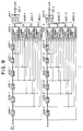
- Fig. 9 shows the configuration of a fourth embodiment of the present invention relating to the radix-2 embodiment shown in Fig. 5 but arranged to perform radix-4 processing.
- input data is successively delayed by delay circuits 62A-1 to 62F-1, each delay circuit delaying the data by N/4.
- the input data is thereby delayed by a total of 3N/2 and is supplied to a first input terminal of a change-over switch 66A-1.
- An output from the delay circuit 62E-1 is supplied to a second input terminal of the change-over switch 66A-1 and to a first input terminal of a change-over switch 66B-1.
- An output from the delay circuit 62D-1 is supplied to each of a third input terminal of the change-over switch 66A-1, a second input terminal of the change-over switch 66B-1 and a first input terminal of a change-over switch 66C-1.
- An output from the delay circuit 62C-1 is supplied to each of a fourth input terminal of the change-over switch 66A-1, a third input terminal of the change-over switch 66B-1, a second input terminal of the change-over switch 66C-1 and a first input terminal of a change-over switch 66D-1.
- An output from the delay circuit 62E-1 is supplied to each of a fourth input terminal of the change-over switch 66B-1, a third input terminal of the change-over switch 66C-1 and a second input terminal of the change-over switch 66D-1.
- An output from the delay circuit 62A-1 is supplied to a fourth input terminal of the change-over switch 66C-1 and to a third input terminal of the change-over switch 66D-1.
- Data input to an input terminal of the delay circuit 62A-1 is supplied to the fourth input terminal of the change-over switch 66D-1.
- Outputs from the change-over switches 66A-1 to 66D-1 are respectively supplied to first to fourth input terminals of a butterfly operation device 64-1.
- An output from the butterfly operation device 64-1 is supplied to a multiplier 63-1 for the twiddle factors.
- An output from the multiplier 63-1 for the twiddle factors is input to a processing circuit forming a subsequent stage.
- Processing circuits forming the second and other subsequent stages are arranged in the same manner. However, the delay time of the delay circuits in each of the subsequent processing stages is 1/4 of that in the preceding stage.
- data is supplied to the first to fourth input terminals of the change-over switch 66A-1 at different times successively shifted by a N/4 step by the delay circuits 62F-1, 62E-1, 62D-1, and 62C-1.
- data is supplied at different times successively shifted by a N/4 step.
- each of the change-over switches 66A-1 to 66D-1 selects, for example, the input to its fourth input terminal to enable groups of data corresponding to the quarters of one symbol to be supplied to the first to fourth input terminals of the butterfly operation device 64-1 simultaneously with each other.
- the butterfly operation device 64-1 performs the first one of necessary butterfly operations.
- the change-over switches 66A-1 to 66D-1 are operated to select the data supplied to the second input terminals and are then operated to select the data supplied to the third input terminals.
- the butterfly operation device 64-1 performs another of the butterfly operations.
- the number of delay circuits in this embodiment is also 2(N - 1).
- Fig. 10 shows an orthogonal frequency division multiplex (OFDM) transmitting and receiving system, which is basically formed of a transmitter 211 and a receiver 231 which receives data transmitted from the transmitter 211 via a transmission path 220.
- OFDM orthogonal frequency division multiplex
- an input symbol string is supplied to an arithmetic unit 202 containing a circuit for inverse fast Fourier transform (inverse FFT) of a pipeline type such as one of those described above.
- inverse FFT can be realized by an arrangement which is basically equal to that for FFT, and which is modified only by the changing the coefficients of multiplications in the multipliers for the twiddle factors from the corresponding coefficients in FFT if the radix is 2. If radix is larger than 2, the arrangement can readily be modified by providing a change-over switch in an input or output section for each butterfly operation device together with changing the multiplication factors.
- a rearrangement circuit 202A for rearranging outputs from the above-mentioned pipeline type inverse FFT circuit is incorporated.
- the rearrangement circuit 202A When the rearrangement circuit 202A is supplied with data, e.g., data items G0 to G15 input successively, it outputs data items, G0, G8, G4, G12, G2, G10, G6, G14, G1, G9, G5, G13, G3, G11, G7, and G15 in this order.
- This output order is determined by bit reverse. That is, if the numbers 0 to 15 indicating the order of data items G0 to G15 are expressed by binary notation, they are 0000, 0001, 0010, ⁇ , 1111. From these binary numbers, binary numbers are obtained by taking the numerals not from the most significant bit but from the least significant bit (bit reversing). The obtained binary numbers express the output order.
- the arithmetic unit 202 processes the input symbol string by inverse FFT.
- the number of points of this inverse FFT is the same as the number of carriers of the input transmitted data modulated by quadrature phase shift keying (QPSK).
- Inverse FFT can be regarded as transform from a frequency region to a time region.
- the output from the arithmetic unit 202 is input to a D/A converter circuit 203 to be converted from digital form into analog form.
- the output from the D/A converter 203 is input to a low-pass filter 204 to extract a time series signal in a base band.
- This signal is input to a multiplier 205 and is multiplied by a carrier output from a carrier generating circuit 206 to be converted into a radio frequency signal at a desired frequency. From this radio frequency signal, a signal in a predetermined pass band is extracted by a band-pass filter 207 to be transmitted through the transmission path 220.
- the receiver 231 only the signal in the predetermined band is extracted from the signal supplied from the transmission path 220 by a band-pass filter 241 and is supplied to a multiplier 242.
- the multiplier 242 multiplies the input signal by a signal at the predetermined frequency output from an oscillator 243 to obtain base band signal components.
- An A/D converter circuit 244 converts the output from the multiplier 242 from analog form into digital form, and outputs the converted signal to an arithmetic unit 245 in which the above-described pipeline type FFT circuit and a rearrangement circuit 245A for rearranging the output from the FFT circuit are incorporated.
- the arithmetic unit 245 processes the input data by FFT processing.
- FFT processing can be regarded as transform from a time region to a frequency region.
- Each of the rearrangement circuits 202A and 245A may be provided in an input section of the pipeline type FFT circuit instead of being provided in an output section.
- the delay time in the processing circuits forming a certain number of processing stages is set in such a manner as to be shortest in the initial stage and to be longer in each subsequent stage than in the preceding stage.
- an OFDM transmitting and receiving system can be realized in which the interval of symbols (symbol value) is increased so that system is not easily affected by a delay time due to reflected waves, and which is therefore strong against multipath interference.
- delay circuits and change-over switches are provided in a stage in front of a butterfly operation device and are arranged so that substantially the same data is input to the butterfly operation device a certain number of times.
- Such an arrangement can be realized as an arrangement other than those of the above-described embodiments.
- the arrangements of the above-described embodiment have a smaller number of delay circuits and correspondingly reduce the manufacturing cost and the size of the arithmetic unit.
Abstract
Description
- The present invention relates to an arithmetic unit and a method for Fourier transform and, more particularly, to an arithmetic unit and a method enabling Fourier transform using a simpler arrangement of butterfly operations.
- Previously, high-speed Fourier transform has been performed by using a software means, i.e., programmed operation of a digital signal processor (DSP). However, since such a software means requires a long processing time, IC chips (special hardware) for performing arithmetic processing for high-speed Fourier transform have recently been brought to use.
- Such hardware means are arranged in such a manner that one butterfly operation circuit is repeatedly used or a plurality of butterfly operation circuits are arranged in parallel with each other.
- If operations are performed by one butterfly operation circuit, a memory (RAM) for storing input data successively processed and a multiplying clock for performing arithmetic processing at a high speed are required.
- In the case where a plurality of butterfly operation circuits are used, a plurality of RAMs for storing intermediate operation results are required.
- If the number N of points of Fourier transform is thereby increased, the circuit scale is increased and a need for external IC chips and a high-speed multiplying clock arises, so that it is difficult for the entire system to be formed in one IC chip.
- Then, processing data in a pipeline processing manner as shown in Fig. 11, for example, may be taken into consideration. In the example shown in Fig. 11, input data is divided into two groups of data: one corresponding to the first half of one symbol (data supplied precedently with respect to time) and the other corresponding to the second half (data supplied by being delayed) by a
distribution switch 1 of a processing circuit forming a first processing stage. The first-half data is supplied to adelay circuit 2 which delays data by an amount of time corresponding to N/2 (N: the number of data items (number of points) of one symbol). After being delayed by N/2, the data is supplied to one (first) input of terminal (shown as an upper input terminal in Fig. 11) of abutterfly operation device 4. - The second-half data separated by the
distribution switch 1 is supplied to amultiplier 3 for the twiddle factors which performs multiplication using complex coefficients stored in a memory such as a ROM (not shown). After undergoing multiplication for the twiddle factors in themultiplier 3, the data is supplied to the other (second) input terminal (shown as a lower input terminal in Fig. 11) of thebutterfly operation device 4. Thebutterfly operation device 4 performs butterfly operation of the two inputs and outputs the result of the operation to a processing circuit forming a subsequent stage (second-stage). - In the second-stage processing circuit, the data output from one (first) output terminal (upper output terminal in Fig. 11) of the first-stage
butterfly operation device 4 is supplied to one (first) input terminal (shown as an upper input terminal in Fig. 11) of a changing switch 6-1 while the data output from the other (second) output terminal (lower output terminal in Fig. 11) of thebutterfly operation device 4 is delayed by N/4 by a delay circuit 5-1 and then supplied to the other (second) input terminal (shown as a lower input terminal in Fig. 11) of the changing switch 6-1. The changing switch 6-1 suitably changes the data input through its two input terminals and outputs the changed data through its two output terminals. - The data output from one (first) output terminal of the changing switch 6-1 is delayed by N/4 by a delay circuit 7-1 and then supplied to one (first) input terminal of a butterfly operation device 9-1. On the other hand, the data output from the other (second) output terminal of the changing switch 6-1 undergoes multiplication for the twiddle factors in a multiplier 8-1 for the twiddle factors and is then supplied to the other (second) input terminal of the butterfly operation device 9-1. The butterfly operation device 9-1 performs butterfly operation of the data input through its two input terminals and outputs the result of the operation through its two output terminals.
- Third-stage and other subsequent processing circuits have the same configuration as the second-stage processing circuit. However, the delay time of delay circuits 5-i and 7-i in the processing circuit forming each intermediate stage is 1/2 of that in the processing circuit forming the preceding stage.
- In the processing circuit forming a stage which is subsequent to the stage in which the delay time of delay circuits 5-k and 7-k is 1 in terms of the number of data items, the data output from one (first) output terminal of butterfly operation device 9-k of the processing circuit forming the preceding stage is supplied directly to one (first) input terminal of a change-over
switch 11 while data output from the other (second) output terminal of butterfly operation device 9-k is delayed by N/2 by a delay circuit 10A and then supplied to the other input terminal of the change-overswitch 11. The change-over switch 11 is arranged to change the data input through the two input terminals into data in serial form and to output this data, and the output from the change-over switch 11 is rearranged by arearrangement circuit 12. - Actually, butterfly operation is achieved by performing both the processing of
butterfly operation device 4 and the processing of themultiplier 3 for the twiddle factors in the first-stage processing circuit, for example. In this specification, for ease of description, processing including no multiplication for the twiddle factors is referred to as butterfly operation (butterfly operation in a narrow sense). - The operation of this processing system will next be described. The
distribution switch 1 divides each of series of data input with respect to unit symbols into first-half data (half data supplied precedently with respect to time) and second-half data (half data supplied after with respect to time). Thedistribution switch 1 supplies the first-half data to thedelay circuit 2 and supplies the second-half data to themultiplier 3 for the twiddle factors. Thedelay circuit 2 delays the input first-half data by N/2 (i.e., an amount corresponding to half data of one symbol) and supplies the delayed data to one of the two input terminal of thebutterfly operation device 4. - At this time, the second-half data, having being output from the
distribution switch 1 and having undergone multiplication for the twiddle factors in themultiplier 3, is supplied to the other input terminal of thebutterfly operation device 4. (The multiplication time of themultiplier 3 for the twiddle factors has been ignored. If this multiplication time is not negligible, the delay time of thedelay circuit 2 is set by also considering this multiplication time. Time setting is also made in the same manner with respect to the other delay circuits.). That is, by virtue of thedelay circuit 2, the first-half data and the second half-data of the same symbol are supplied to thebutterfly operation device 4 by the same timing to be input thereto simultaneously with each other (the items of each of the first-half data and second-half data being input one by one in order from the leading item). Thebutterfly operation device 4 performs radix-2 butterfly operation with respect to corresponding data items of the two groups of input data. - Fig. 12 shows the principle of radix-2 butterfly operation. In the example of operation shown in Fig. 12, the number N of data items of one symbol is 16.
- That is, the
butterfly operation device 4 adds the first one of first-half data items represented bynumbers 0 to 7, i.e.,data item 0, and the first one of second-half data items represented bynumbers 8 to 15, i.e.,data item 8, in sixteen data items constituting a symbol g and represented bynumbers 0 to 15 in Fig. 12. Thebutterfly operation device 4 also performs subtraction between thedata items data item 0 in a column p shown in Fig. 12 while the value obtained by the subtraction is set as adata item 8 in column p. - Next, the sum and the difference between the second one of the first-half data items of the symbol g, i.e.,
data item 1, and the second one of the second-half data items of the symbol g, i.e.,data item 9, are calculated. The sum is set asdata item 1 in column p while the difference is set asdata item 9 in column p. The subsequent data items are processed in the same manner. Thus, sixteen data items represented bynumbers 0 to 15 in column p are obtained. The group of eight data items in the first half of column p, represented bynumbers 0 to 7, and the group of eight data items in the second half of column p, represented bynumbers 8 to 15, are supplied in parallel with each other to the processing circuit forming the subsequent stage, each group of data items being sent in serial order. - In the second-stage processing circuit, eight
data items 0 to 7 in the first half of column p, output from the first-stagebutterfly operation device 4, are supplied directly to one of the two input terminals of the changing switch 6-1 while eightdata items 8 to 15 in the second half are input to the delay circuit 5-1. The data items input to the delay circuit 5-1 are delayed by N/4 (i.e., an amount corresponding to a quarter of the symbol) and then supplied to the other input terminal of the changing switch 6-1. - The changing switch 6-1 executes processing for suitably changing the data items supplied to the two input terminals shown as upper and lower terminals in Fig. 11.
- That is, as shown in Fig. 12, first-half four
data items 0 to 3 in column-p data items 0 to 7 supplied through the upper input terminal are supplied to the delay circuit 7-1. Following second-half fourdata items 4 to 7 in column-p data items 0 to 7 are output to the multiplier 8-1 for the twiddle factors. Four column-p data items 8 to 11 which are supplied to the lower input terminal of the changing switch 6-1 when four column-p data items 4 to 7 are supplied to the upper input terminal of the changing switch 6-1 are supplied to the delay circuit 7-1. Four column-p data items 12 to 15, input subsequently, are supplied to the multiplier 8-1 for the twiddle factors. - That is,
data items 0 to 3 and 8 to 11 are successively output from the first output terminal of the changing switch 6-1 whiledata items 4 to 7 and 12 to 15 are successively output from the second output terminal. - The delay circuit 7-1 delays four input column-
p data items 0 to 3 by N/4 and supplies these data items to one of the two input terminals of the butterfly operation device 9-1. At this time, fourdata items 4 to 7 which have undergone multiplication for the twiddle factors in the multiplier 8-1 are supplied to the other input terminal of the butterfly operation device 9-1. That is, by virtue of the delay circuit 7-1,data items 0 to 3 anddata items 4 to 7 are supplied to the butterfly operation device 9-1 by the same timing to be input thereto simultaneously with each other. - The butterfly operation device 9-1 calculates the sum and difference between column-
p data items data item 0 in column q and sets the difference asdata item 4 in column q. The butterfly operation device 9-1 also calculates the sum and difference between column-p data items data item 1 in column q and sets the difference asdata item 5 in column q. The same processing is repeated to obtain eight column-q data items 0 to 7 from column-p data items 0 to 7. - After delaying four input column-
p data items 0 to 3 by N/4, the delay circuit 7-1 delays four subsequently-input data items 8 to 11 by N/4 and supplies these data items to the above-mentioned one input terminal of the butterfly operation device 9-1. At this time, fourdata items 12 to 15 which have undergone multiplication for the twiddle factors in the multiplier 8-1 are supplied to the other input terminal of the butterfly operation device 9-1. That is, fourdata items 8 to 11 and fourdata items 12 to 15 are supplied to the two input terminals of the butterfly operation device 9-1 by the same timing to be input thereto simultaneously with each other. - The butterfly operation device 9-1 calculates the sum and difference between column-
p data items data item 8 in column q and sets the difference asdata item 12 in column q. The butterfly operation device 9-1 also calculates the sum and difference between column-p data items data item 9 in column q and sets the difference asdata item 13 in column q. - The subsequent column-p data items are processed in the same manner. Thus, eight column-
q data items 8 to 15 are obtained from eight column-p data items 8 to 15. - Column-
q data items 0 to 7 and 8 to 15 output from the second-stage butterfly operation device 9-1 are input to the third-stage processing circuit in parallel with each other. - Similar processing is subsequently performed in the third-stage and subsequent processing circuits.
- Of the data processed by the butterfly operation device 9-k in the processing circuit forming the stage including the delay circuits 5-k and 7-k for delaying data by an amount corresponding to one data item, the data output from the upper output terminal of the butterfly operation device 9-k as shown in Fig. 11 is supplied to the upper input terminal of the change-
over switch 11 while the data output from the lower output terminal of the butterfly operation device 9-k is delayed by N/2 by the delay circuit 10A and then supplied to the lower input terminal of the change-over switch 11. - The change-
over switch 11 first selects andoutputs data items over switch 11 next selects andoutputs data items rearrangement circuit 12 rearrange these data items into a sequence, e.g., 0, 8, 4, 12, 2, 10, 6, 14, 1, 9, 5, 13, 3, 11, 7, 15 (by so-called bit reverse processing mentioned below in the description of an embodiment of the present invention) and outputs this sequence of data items. - The above-described sequence of operation is repeated. Thus, serial data input to the
distribution switch 1 is successively processed in a pipeline processing manner through the processing stages by being divided into groups of data items processed in parallel with each other, and the processed data items are again changed into serial data by the change-over switch 11. This serial data is output at the same clock rate as the serial data input to thedistribution switch 1. - The
distribution switch 1, the changing switch 6-1 to 6-k and the change-over switch 11 in the processing stages are controlled by predetermined timing by a timing control circuit (not shown). - The number of delay circuits required in this example is 2(N - 1).
- In the example shown in Fig. 11, the multiplier 8-i for the twiddle factors (multiplier 3) in each stage is inserted between the lower output terminal of the changing switch 6-i (distribution switch 1) and the lower input terminal of the butterfly operation device 9-i (butterfly operation device 4), as shown in Fig. 13. Alternatively, it may be connected to the lower output terminal of the butterfly operation device 9-i, as shown in Fig. 14.
- Further, the multiplier 8-i for the twiddle factors may alternatively be inserted between the delay circuit 5-i and the lower input terminal of the changing switch 6-i. In each case, the same operation result can be obtained as in the case of using the arrangement shown in Fig. 13. However, multiplying values of multiplication for the twiddle factors are changed according to the inserted position.
- Fig. 16 shows an example of radix-4 butterfly operation relating to radix-2 butterfly operation of the processing system shown in Fig. 11. In this example, a first-
stage distribution switch 11 divides data of each of input symbols into quarters and outputs the divided data items. The first quarter of the data is delayed by N/4 by each ofdelay circuits butterfly operation device 14. The second quarter of the data is delayed by N/4 by each ofdelay circuits multiplier 13A for the twiddle factors. Themultiplier 13A multiplies the input data by complex coefficients stored in a memory such as a ROM (not shown) and supplies the result of this multiplication to a second input terminal of thebutterfly operation device 14. - The third quarter of the data output from the
distribution switch 11 is delayed by N/4 by adelay circuit 12F and then input to amultiplier 13B for the twiddle factors. Themultiplier 13B performs multiplication of the input data with respect to the twiddle factors and supplies the result of this multiplication to a third input terminal of thebutterfly operation device 14. The fourth quarter of the data output from thedistribution switch 11 undergoes multiplication for the twiddle factors performed by amultiplier 13C for the twiddle factors and is then supplied to a fourth input terminal of thebutterfly operation device 14. - The
butterfly operation device 14 performs butterfly operation of the groups of data input through the four input terminals and successively outputs each of the four parallel groups of data to a second-stage processing circuit. - In the second-stage processing circuit, the data output from a first output terminal of the first-stage
butterfly operation device 14 is input directly to a first input terminal of a changing switch 16-1. The data output from a second output terminal of thebutterfly operation device 14 is delayed by N/16 by adelay circuit 15F-1 and then supplied to a second input terminal of the changing switch 16-1. The data output from a third output terminal of thebutterfly operation device 14 is delayed by N/16 by each ofdelay circuits 15D-1 and 15E-1, that is, delayed by N/8 in total and then supplied to a third input terminal of the changing switch 16-1. The data output from a fourth output terminal of thebutterfly operation device 14 is delayed by N/16 by each ofdelay circuits 15A-1, 15B-1, and 15C-1, that is, delayed by 3N/16 in total and then supplied to a fourth input terminal of the changing switch 16-1. - The changing switch 16-1 suitably selects data items input through its four input terminals and outputs the selected data items through its four output terminals.
- The data output from the first output terminal of the changing switch 16-1 is delayed by N/16 by each of
delay circuits 17A-1, 17B-1, and 17C-1, that is, delayed by 3N/16 in total and then supplied to a first input terminal of a butterfly operation device 19-1. The data output from the second output terminal of the changing switch 16-1 is delayed by N/16 by each ofdelay circuits 17D-1 and 17E-1, that is, delayed by N/8 in total and then input to amultiplier 18A-1 for the twiddle factors. Themultiplier 18A-1 performs multiplication of the input data with respect to the twiddle factors and supplies the result of this multiplication to a second input terminal of the butterfly operation device 19-1. - The data output from the third output terminal of the changing switch 16-1 is delayed by N/16 by a
delay circuit 17F-1 and then input to amultiplier 18B-1 for the twiddle factors. Themultiplier 18B-1 performs multiplication of the input data with respect to the twiddle factors and supplies the result of this multiplication to a third input terminal of the butterfly operation device 19-1. The data output from the fourth output terminal of the changing switch 16-1 undergoes multiplication for the twiddle factors performed by amultiplier 18C-1 for the twiddle factors and is then supplied to a fourth input terminal of the butterfly operation device 19-1. - Similar processing is performed in each of subsequent stages to successively process the data. In the example shown in Fig. 11, the delay time of the delay circuits in each stage is 1/2 of that of the delay circuits in the preceding stage. In contrast, in this example, the delay time of each stage is 1/4 of that of the preceding stage.
- The data output from each of first to fourth output terminals of a butterfly operation device 19-k in a stage in which the delay time of delay circuits corresponds to one data item is supplied to the corresponding one of first to fourth input terminals of a change-
over switch 21 directly or after being delayed by N/4 by adelay circuit 20F,delay circuits delay circuits 20A to 20C. The change-over switch 21 suitably selects data items input through the first to fourth terminals in parallel with each other and outputs the selected data items as serial data. Arearrangement circuit 22 rearranges outputs from the change-over switch 11 and outputs rearranged data. - The operation of this processing system will next be described. The
distribution switch 11 divides each of series of data input with respect to unit symbols into four groups and outputs the divided groups of data through the first to fourth output terminals. For example, if one symbol is constituted of 16 data items as shown in Fig. 17, four data items of symbol g represented bynumbers 0 to 3 are output through the first terminal; four data items represented bynumbers 4 to 7, through the second output terminal; four data items represented bynumbers 8 to 11, through the third output terminal; and four data items represented bynumbers 12 to 15, through the fourth output terminal. - Four
data items 0 to 3 ahead of the others with respect to time are delayed by a total of 3N/4 by thedelay circuits butterfly operation device 14. Fourdata items 4 to 7 are delayed by a total of N/2 by thedelay circuits multiplier 13A for the twiddle factors, and are supplied to the second input terminal of thebutterfly operation device 14. - Four
data items 8 to 11 are delayed by N/4 by thedelay circuit 12F and then input to themultiplier 13B for the twiddle factors. These data items are supplied to the third input terminal of thebutterfly operation device 14 after undergoing multiplication for the twiddle factors. Fourdata items 12 to 15 undergo multiplication for the twiddle factors in themultiplier 13C for the twiddle factors and are thereafter supplied to the fourth input terminal of thebutterfly operation device 14. Thus, the groups of four data items are respectively supplied to the four input terminals of thebutterfly operation device 14 by the same timing to be input thereto simultaneously with each other, the data items in each group being input in serial order. - The
butterfly operation device 14 performs butterfly operation ofdata items data items - Next, butterfly operation of
data items data items - The subsequent data items of symbol g are processed in the same manner. Thus, sixteen data items in column p are calculated from the sixteen data items of symbol g. These operation results are output to the second-stage processing circuit.
- In the second processing circuit, p-
column data items 0 to 3 are supplied to the first terminal of the changing switch 16-1, and column-p data items 4 to 7 are delayed by N/16 by thedelay circuit 15F-1 and then supplied to the second input terminal.Data items 8 to 11 are delayed by a total of N/8 by thedelay circuits 15D-1 and 15E-1 and then supplied to the third input terminal.Data items 12 to 15 are delayed by a total of 3N/16 by thedelay circuits 15A-1, 15B-1, and 15C-1 and then supplied to the fourth input terminal. - The changing switch 16-1 first selects column-
p data item 0 output from the first output terminal of thebutterfly operation device 14 and input through the first input terminal of the changing switch 16-1, and outputs this data item through the first output terminal.Data item 0 output from the first output terminal of the changing switch 16-1 is delayed by 3N/16 by thedelay circuits 17A-1, 17B-1, and 17C-1 and then supplied to the first input terminal of the butterfly operation device 19-1. - At the next input time,
data items Data item 1 is output through the second output terminal whiledata item 4 is output through the first output terminal. - Similarly,
data items data items data items data items data item 15 is output through the fourth output terminal. - Column-
p data items delay circuits 17A-1, 17B-1, and 17C-1, and are then supplied to the first input terminal of the butterfly operation device 19-1. - Column-
p data items delay circuits 17D-1 and 17E-1, thereafter undergo multiplication for the twiddle factors performed by themultiplier 18A-1 for the twiddle factors, and are then supplied to the second input terminal of the butterfly operation device 19-1. - Column-
p data items delay circuit 17F-1, thereafter undergo multiplication for the twiddle factors performed by themultiplier 18B-1 for the twiddle factors, and are then supplied to the third input terminal of the butterfly operation device 19-1. Column-p data items multiplier 18C-1 for the twiddle factors, and are supplied to the fourth input terminal of the butterfly operation device 19-1. - As described above, column-
p data items 0 to 3 are respectively supplied to the first to fourth input terminals of the butterfly operation device 19-1 by the same timing to be input thereto simultaneously with each other. The butterfly operation device 19-1 performs butterfly operation of these four data items to formdata items 0 to 3 in column G. - Similarly, when
data items data items 4 to 7 in column G. Also, whendata items items 8 to 11 or 12 to 15 in column G shown in Fig. 17 are obtained from the first to fourth output terminals of the butterfly operation device 19-1. - If the number of data items of one symbol is sixteen, the operation of the butterfly operation devices is completed by the above-descried processing. If the number of data items of one symbol is larger than sixteen, the same processing is performed in other one or more subsequent processing circuits.
- Of the four column-
G data items 0 to 4 with which butterfly operation has been completed,data item 0 is supplied to the first input terminal of the change-over switch 21 without being delayed.Data item 1 is delayed by N/4 by thedelay circuit 20F,data item 2 is delayed by N/2 by thedelay circuit data item 3 is delayed by 3N/4 by thedelay circuits over switch 21. - The change-
over switch 21 selects andoutputs data items outputs data items over switch 21 selects andoutputs data items data items - By repeating this operation, the data items are output in serial form and are rearranged in the order from 0 to 15 in the
rearrangement circuit 22. - In the case of the system shown in Fig. 11, in which the radix is 2, the number of delay circuits is 2(N - 1). In the case of the system shown in Fig. 16, in which the radix is 4, the number of delay circuits is 4(N - 1). (If the radix is R, the number of delay circuits is R(N - 1).
- In either example, the position of the multipliers for the twiddle factors is not restricted and there is no limit to the radix of fast Fourier transform. Further, there is no restriction on setting the amount of delay. In each of the above-described examples, series of data are input to or output from each stage in parallel with each other.
- Thus, in the conventional Fourier transform arithmetic unit, a plurality of operations are performed by each butterfly operation device at a time. Accordingly, the construction of each butterfly operation device is complicated, so that the overall size of the arithmetic unit is large and the cost for manufacturing the arithmetic unit is high.
- In view of these circumstances, an object of the present invention is to provide an arithmetic unit and a method which enable Fourier transform using simpler butterfly operation devices such that the size and the manufacturing cost of the arithmetic unit are reduced.
- To achieve this object, according to one aspect of the present invention, there is provided a Fourier transform arithmetic unit comprising a plurality of processing stages for performing fast Fourier transform by pipeline processing, each of the plurality of processing stages having timing control means for dividing input data responding to one symbol into a plurality of groups of data and for outputting the plurality of divided groups of data a certain number of times by the same timing, and first operation means supplied with the plurality of groups of data output a certain number of times by the same timing by the timing control means, the first operation means performing predetermined operation each time the plurality of groups of data are input, the first operation means outputting a result of butterfly operation in a time division manner.
- According to another aspect of the present invention, there is provided a Fourier transform operation method of performing fast Fourier transform by pipeline processing using a plurality of processing stages, the method comprising, in each of the plurality of processing stages, a first step of dividing input data corresponding to one symbol into a plurality of groups of data, a second step of outputting the plurality of divided groups of data a certain number of times by the same timing, and a third step of performing predetermined operation each time the plurality of groups of data are supplied by the same timing, and outputting a result of butterfly operation in a time division manner.
- The present invention will be more clearly understood from the following description, given by way of example only, with reference to the accompanying drawings in which:
- Fig. 1 is a block diagram showing the configuration of a first embodiment of a Fourier transform arithmetic unit in accordance with the present invention;
- Fig. 2 is a diagram of the operation of the embodiment shown in Fig. 1;
- Fig. 3 is a block diagram showing the configuration of a second embodiment of the Fourier transform arithmetic unit of the present invention;
- Fig. 4 is a diagram of the operation of the embodiment shown in Fig. 3;
- Fig. 5 is a block diagram showing the configuration of a third embodiment of the Fourier transform arithmetic unit of the present invention;
- Fig. 6 is a diagram of the operation of the embodiment shown in Fig. 5;
- Fig. 7 is a diagram of the change-over operation of a change-over switch in the embodiment shown in Fig. 5;
- Fig. 8 is a block diagram showing the configuration of a Fourier transform arithmetic unit in accordance with a seventh embodiment of the present invention;
- Fig. 9 is a block diagram showing the configuration of a fourth embodiment of the Fourier transform arithmetic unit of the present invention;
- Fig. 10 is a block diagram showing the configuration of an example of an OFDM (orthogonal frequency division multiplex) transmitting and receiving system to which the Fourier transform arithmetic unit of the present invention is applied;
- Fig. 11 is a block diagram showing the configuration of an example of a Fourier transform arithmetic unit;
- Fig. 12 is a diagram of an algorithm for radix-2 fast Fourier transform;
- Fig. 13 is a diagram showing the inserted position of the multiplier for the twiddle factors in the example shown in Fig. 11;
- Fig. 14 is a diagram showing another example of the inserted position of the multiplier for the twiddle factors;
- Fig. 15 is a diagram showing still another example of the inserted position of the multiplier for the twiddle factors;
- Fig. 16 is a block diagram showing the configuration of another example of the Fourier transform arithmetic unit; and
- Fig. 17 is a diagram of an algorithm for fast Fourier transform in a case where the radix is 4.
- Fig. 1 is a block diagram showing the configuration of a first embodiment of a Fourier transform arithmetic unit in accordance with the present invention. In this embodiment, a distribution switch 31-1 of a processing circuit forming an initial stage divides input data into first-half data preceding with respect to time and second-half data following the first-half data. The first-half data is supplied to a
delay circuit 32A-1 via a second input terminal of a change-over switch 36A-1. An output from thedelay circuit 32A-1 obtained by delaying the data by N/2 (N: the number of data items of one symbol) is again input to thedelay circuit 32A-1 via a first input terminal of the change-overswitch 36A-1. - Similarly, the second-half data distributed by the distribution switch 31-1 is input to a
delay circuit 32B-1 via a first input terminal of a change-over switch 36B-1. The data output from thedelay circuit 32B-1 after being delayed by N/2 by this circuit is again input to thedelay circuit 32B-1 via a second input terminal of the change-over switch 36B-1. - A butterfly operation device 34-1 fetches the data output from the
delay circuit 32A-1 and the data output from the change-over switch 36B-1, performs butterfly operation using these groups of data and outputs the result of this operation to a multiplier 33-1 for the twiddle factors. The multiplier 33-1 performs multiplication of the input data with respect to the twiddle factors and outputs the result of this multiplication to a processing circuit forming a subsequent stage. - Processing circuits forming the second and other subsequent processing stages are arranged in the same manner as the first-stage processing circuit. However, the delay time of the delay circuits in each of the subsequent processing stages is 1/2 of that in the preceding stage.
- The operation of this embodiment will next be described with reference to Fig. 2. The distribution switch 31-1 divides input data corresponding to each of unit symbols into first-half data and second-half data (Fig. 2(A)), supplies the first-half data to the second input terminal of the change-over
switch 36A-1 (Fig. 2(B)) and supplies the second-half data to the first input terminal of the change-over switch 36B-1 (Fig. 2(C)). - The data input to the change-over
switch 36A-1 through the second input terminal of this switch is supplied and written to thedelay circuit 32A-1. For example, as shown in Fig. 2(B), first-half data f0 of a symbol f is written to thedelay circuit 32A-1. After an elapse of a delay time corresponding to N/2, this data f0 is read out from thedelay circuit 32A-1 to be supplied to the first input terminal of the butterfly operation device 34-1. - Second-half data f1 distributed by the distribution switch 31-1 is input to the change-
over switch 36B-1 through the first input terminal of this switch by the same timing as data f0 supplied to the first input terminal of the butterfly operation device 34-1. Second-half data f1 is thereby supplied to the second input terminal of the butterfly operation device 34-1. The butterfly operation device 34-1 performs one of two necessary operations, e.g., addition (f0 + f1) with respect to first-half data f0 and second-half data f1 simultaneously input to its two input terminals and outputs the result of this operation (Fig. 2(F)). - While a sequence of operation of first-half data f0 is being performed by the butterfly operation device 34-1, first-half data f0 read out from
delay circuit 32A-1 is again written to thedelay circuit 32A-1 via the first input terminal of the change-overswitch 36A-1 (Fig. 2(D)). Similarly, second-half data f1 output from the change-over switch 36B-1 is written to thedelay circuit 32B-1 (Fig. 2(E)) while the operation of this data is being performed by the butterfly operation device 34-1. When the butterfly operation device 34-1 finishes the addition of first-half data f0 and second-half data f1, first-half data f0 is again output from thedelay circuit 32A-1 and second-half data f1 is read out from thedelay circuit 32B-1. These first-half data f0 and second-half data f1 are output through the change-over switch 36B-1. Thus, the same data is again input to the butterfly operation device 34-1. - The butterfly operation device 34-1 performs the other of its operations not performed at the preceding time, e.g., subtraction (f0 - f1) of first-half data f0 and second-half data f1 again input and outputs the result of this operation.
- When first-half data f0 is being read out from the
delay circuit 32A-1, first-half data g0 of the next symbol g is supplied from the distribution switch 31-1 and written to thedelay circuit 32A-1 via the second input terminal of the change-overswitch 36A-1. Thus, butterfly operation can be performed continually with respect to the data of input symbols. - The result of butterfly operation performed by the butterfly operation device 34-1 is input to the multiplier 33-1 for the twiddle factors. After undergoing multiplication for the twiddle factors, the operation result is output to the processing circuit forming the subsequent stage.
- Similar processing is performed in the processing circuits forming the second and other subsequent stages.
- In this embodiment, as described above, butterfly operation is performed in the butterfly operation device 34-1 in a time division manner. It is sufficient for the butterfly operation device 34-1 to perform one operation (addition or subtraction) at a time. Therefore, the scale of the circuit of the present invention can be reduced in comparison with the circuit arranged to perform two operations (both addition and subtraction) at a time. The number of delay circuits in this embodiment is 2(N - 1).
- Fig. 3 shows the configuration of another embodiment of the present invention in which radix-4 operation relating to the radix-2 operation of the embodiment of radix-2 operation shown in Fig. 1 is performed. In this embodiment, a
distribution switch 41A-1 divides input data into quarters and outputs the divided data through its first to fourth output terminals. It is necessary for the data output from the first output terminal of thedistribution switch 41A-1 to be delayed by a total of 3N/4 before being supplied to a first input terminal of a butterfly operation device 44-1. It is necessary for the data output from the second output terminal to be delayed by N/2 before being supplied to a second input terminal of the butterfly operation device 44-1. It is necessary for the data output from the third output terminal to be delayed by N/4 before being supplied to a third input terminal of the butterfly operation device 44-1. Finally, it is necessary for the data output from the fourth output terminal to be supplied to the fourth input terminal of the butterfly operation device 44-1 without being specially delayed. - Therefore, the data output from the first output terminal of the
distribution switch 41A-1 in a processing circuit forming an initial stage is supplied to a second input terminal of a change-over switch 46A-1 or to a second input terminal of achangeover switch 46B-1 via a first or second output terminal of a distribution switch 41B-1. - The change-over
switch 46A-1 selects one of an output from adelay circuit 42A-1 which delays data by N/4 and an output from a first output terminal of the distribution switch 41B-1, and supplies the selected data to thedelay circuit 42A-1. The change-over switch 46B-1 selects one of an output from adelay circuit 42B-1 which delays data by N/4 and an output from a second output terminal of the distribution switch 41B-1, and outputs the selected data to thedelay circuit 42B-1. A change-over switch 46F-1 selects one of an output from adelay circuit 42A-1 and an output from thedelay circuit 42B-1 and supplies the selected data to the first input terminal of the butterfly operation device 44-1. - A change-
over switch 46C-1 selects one of the data output from the second output terminal of thedistribution switch 41A-1 and an output from adelay circuit 42C-1 which delays data by N/4. The change-overswitch 46C-1 outputs the selected data to thedelay circuit 42C-1. Adelay circuit 42E-1 delays an output from thedelay circuit 42C-1 and supplies the delayed data to the second input terminal of the butterfly operation device 44-1. - A change-
over switch 46D-1 selects one of the data output from the third output terminal of thedistribution switch 41A-1 and data output from adelay circuit 46D-1 which delays data by N/4. The change-over switch 46D-1 supplies the selected data to thedelay circuit 46D-1. An output from thedelay circuit 46D-1 is supplied to the third input terminal of the butterfly operation device 44-1. - A change-
over switch 46E-1 selects one of the data output from the fourth output terminal of thedistribution switch 41A-1 and data output from adelay circuit 42F-1 which delays data by N/4. The change-overswitch 46E-1 supplies the selected data to thedelay circuit 46D-1 and to the fourth input terminal of the butterfly operation device 44-1. - One output from the butterfly operation device 44-1 is input to a multiplier for the twiddle factors 43-1. After undergoing multiplication for the twiddle factors, the data is output to a processing circuit forming a subsequent stage.
- Processing circuits forming the second and other subsequent stages are arranged in the same manner. However, the delay time of the delay circuits in each of the subsequent processing stages is 1/4 of that in the preceding stage.
- The operation of this arithmetic unit will next be described with reference to Fig. 4. The initial-
stage distribution switch 41A-1 divides input data corresponding to each of unit symbols (Fig. 4(A)) into quarters. For example, thedistribution switch 41A-1 divides a symbol f into first-quarter data f0, second-quarter data f1, third-quarter data f2 and fourth-quarter data f3. Thedistribution switch 41A-1 outputs these groups of data through its first to fourth output terminals (Figs. 4(B) to 4(E)). - The data output from the first output terminal of the
distribution switch 41A-1 is input to the distribution switch 41B-1 to be supplied to the change-overswitch 46A-1 or to the change-over switch 46B-1. The distribution switch 41B-1 distributes input data to the change-overswitch 46A-1 and to the change-over switch 46B-1 alternately with respect to unit symbols. For example, if the data of symbol f is supplied to the change-overswitch 46A-1, the data of the next symbol g is output to the change-over switch 46B-1. The data of the next but one symbol h is again supplied to the change-overswitch 46A-1. - For example, data f0 of the first symbol f is supplied to the change-over
switch 46A-1. The change-overswitch 46A-1 supplies this data to thedelay circuit 42A-1 to write the data to this delay circuit (Fig. 4(F)). Data f0 written to thedelay circuit 42A-1 is delayed by N/4 and then read out to be again input to thesame delay circuit 42A-1 through the change-overswitch 46A-1. When data f0 is delayed by a total of 3N/4 by repeating this operation, it is supplied to the first input terminal of the butterfly operation device 44-1 through the change-overswitch 46F-1. - Second-quarter data f1 output from the second output terminal of the
distribution switch 41A-1 is input and written to thedelay circuit 42C-1 through the change-overswitch 46C-1 (Fig. 4(H)). Thedelay circuit 42C-1 delays the input data by N/4 and outputs the delayed data. This data f1 output from thedelay circuit 42C-1 is again input and written to thedelay circuit 42C-1 through the change-overswitch 46C-1. This operation is repeatedly performed. - The
delay circuit 42E-1 further delays by N/4 the data delayed by N/4 by thedelay circuit 42C-1 and supplies the data to the second input terminal of the butterfly operation device 44-1 (Fig. 4(J)). Accordingly, data f1 is input to the second terminal of the butterfly operation device 44-1 when data f0 is input to the first input terminal of the butterfly operation device 44-1. - Third-quarter data f2 output from the third output terminal of the
distribution switch 41A-1 is input and written to thedelay circuit 42D-1 via the second input terminal of the change-over switch 46D-1 (Fig. 4(I)). After being delayed by N/4 by thedelay circuit 42D-1, data f2 is again input to thedelay circuit 42D-1 via the first input terminal of the change-over switch 46D-1 to be delayed. This operation is repeatedly performed. - As a result, data f2 from the
delay circuit 42D-1 is supplied to the third input terminal of the butterfly operation device 44-1 when data f0 and data f1 are supplied to the first and second input terminals of the butterfly operation device 44-1. - Fourth-quarter data f3 output from the fourth output terminal of the
distribution switch 41A-1 is written to thedelay circuit 42F-1 via the first input terminal of the change-overswitch 46E-1 (Fig. 4(K)) and is simultaneously supplied to the fourth input terminal of the butterfly operation device 44-1. - In the above-described manner, groups of data f0 to f3 as the quarters of symbol f are supplied to the first to fourth input terminals of the butterfly operation device 44-1 simultaneously with each other, data items in each group being input in serial order. The butterfly operation device 44-1 performs predetermined one of four butterfly operations which are to be performed with respect to the four groups of data f0 to f3, and outputs operation result F0 (Fig. 4(L)).
- Data f0 is again supplied from the
delay circuit 42A-1 to the first input terminal of the butterfly operation device 44-1 through the change-overswitch 46F-1 at the time of the next input subsequent to the time when the butterfly operation device 44-1 finishes outputting the operation result F0 (Fig. 4(F)). Similarly, data f1 is supplied from thedelay circuit 42E-1 to the second input terminal (Fig. 4(J)), data f2 is supplied from thedelay circuit 42D-1 to the third input terminal (Fig. 4(I)) and data f3 is supplied from thedelay circuit 42F-1 to the fourth input terminal via the change-overswitch 46E-1 (Fig. 4(K)). - Then the butterfly operation device 44-1 performs the second one of the four butterfly operations and outputs operation result F1 (Fig. 4(L)).
- When the second operation result F1 is completed by the same operation, data f0 and data f3 are again input to the first to fourth input terminals of the butterfly operation device 44-1. The butterfly operation device 44-1 then outputs operation result F2 of the third butterfly operation. When outputting operation result F2 is completed, data f0 to data f3 are again input to undergo the fourth butterfly operation, thereby outputting operation result F3.
- When the butterfly operation device 44-1 finishes outputting the first operation result F0 of symbol f, groups of data g0 to g3 as the quarters of the next symbol g are successively output from the first to fourth output terminals of the
distribution switch 41A-1, one preceding the next by N/4. - The first data g0 cannot be supplied and written to the
delay circuit 42A-1. That is, it is still necessary for thedelay circuit 42A-1 to hold data f0 and to supply this data to the butterfly operation device 44-1. Therefore, the distribution switch 41B-1 supplies data g0 to thedelay circuit 42B-1 through the change-over switch 46B-1, thereby writing the data to thedelay circuit 42B-1 (Fig. 4(G)). Thedelay circuit 42B-1 delays the input data g0 by N/4 and outputs the delayed data. This delayed data g0 is again input to thedelay circuit 42B-1 through the change-over switch 46B-1 to be delayed. This operation is repeatedly executed. - When the last quarter data g3 of symbol g is output from the fourth output terminal of the
distribution switch 41A-1 and input to the fourth input terminal of the butterfly operation device 44-1, data g0 read out from thedelay circuit 42B-1 is supplied to the first input terminal of the butterfly operation device 44-1 through the change-overswitch 46F-1. Similarly, at this time, data g1 and data g2 output from the second and third output terminals of thedistribution switch 41A-1 are read out from thedelay circuit 42E-1 and thedelay circuit 42D-1 to be supplied to the second and third input terminals of the butterfly operation device 44-1. The butterfly operation device 44-1 then performs the first one of the butterfly operations with respect to the input data g0 and g3 and outputs operation result G0 (Fig. 4(L)). - Subsequently, the butterfly operations are performed in the time division manner to output operation results.
- The data output from the butterfly operation device 44-1 is input to the multiplier 43-1 for the twiddle factors. After undergoing multiplication for twiddle factors, the data is output to the processing circuit forming the subsequent stage.
- Processing similar to that of the first-stage processing circuit is performed in each of the second-stage and other subsequent processing circuits.
- The number of delay circuits in this embodiment is 2(N - 1).
- Fig. 5 shows a third embodiment of the present invention in which radix-2 fast Fourier transform is performed. In this embodiment, no distribution switch corresponding to the distribution switch 31-1 of the embodiment shown in Fig. 1 is used and input data is successively delayed by
delay circuits 52A-1 and 52B-1 instead of being distributed by a distribution switch before it is input to a first input terminal of a change-over switch 56A-1. Each of thedelay circuits 52A-1 and 52B-1 delays the data by N/2. An output from thedelay circuit 52A-1 is supplied to a second input terminal of the change-overswitch 56A-1. - The output from the
delay circuit 52A-1 is also supplied to a first input terminal of a change-over switch 56B-1. Data input to an input terminal of thedelay circuit 52A-1 is supplied to a second input terminal of the change-over switch 56B-1. Data selected by the change-overswitches 56A-1 and 56B-1 is supplied to first and second input terminals of a butterfly operation device 54-1. An output from the butterfly operation device 54-1 undergoes operation for the twiddle factors performed by an operation device 53-1 and is thereafter output to a processing circuit forming a subsequent stage. - Processing circuits forming the second and other subsequent stages are arranged in the same manner as the initial-stage processing circuit. However, the delay time of the delay circuits in each of the subsequent processing stages is 1/2 of that in the preceding stage.
- The operation of this embodiment will next be described with reference to Fig. 6. If, for example, data of a symbol f (Fig. 6(A)) is input, first-half data f0 delayed by N/2 by the
delay circuit 52A-1 is supplied to the second input terminal of the change-overswitch 56A-1 (Fig. 6(B)). On the other hand, second-half data f1 is supplied to the second input terminal of the change-over switch 56B-1 (Fig. 6(A)). Then, as shown in Fig. 7, each of the change-overswitches 56A-1 and 56B-1 is changed to the lower position as seen in the figure to supply first-half data f0 to the first input terminal of the butterfly operation device 54-1 (Fig. 6(D)) and to simultaneously supply second-half data f1 to the second input terminal of the butterfly operation device 54-1 (Fig. 6(E)). The butterfly operation device 54-1 performs the first one of two butterfly operations, e.g., addition and outputs the value of the addition result (f0 + f1) (Fig. 6(F)). - Next, the change-over
switches 56A-1 and 56B-1 are changed to the upper positions as seen in the figure. The change-overswitch 56A-1 thereby fetches first-half data f0 delayed by a total of N by thedelay circuits 52A-1 and 52B-1 (Fig. 6(C)). Also, the change-over switch 56B-1 fetches second-half data f1 delayed by N/2 by thedelay circuit 52A-1 (Fig. 6(B)). The butterfly operation device 54-1 performs the other butterfly operation not performed at the preceding time, e.g., subtraction and outputs the value of the subtraction result (f0 - f1) (Fig. 6(F)). - Similar processing is performed in the processing circuits forming the second and other subsequent stages.
- The embodiment shown in Fig. 5 may alternatively be such that, for example, as shown in Fig. 8, only one change-
over switch 56 is provided in one stage, the output of thedelay circuit 52B-1 is supplied to the first input terminal of the change-over switch 56, the output of thedelay circuit 52A-1 is supplied directly to the first input terminal of the butterfly operation device 54-1, and the data supplied to the input terminal of thedelay circuit 52A-1 is supplied to the second input terminal of the change-over switch 56. (The processing circuits of the other stages are arranged in the same manner.) - In such a case, when first-half data f0 is supplied first time from the
delay circuit 52A-1 to the first input terminal of the butterfly operation device 54-1, second-half data f1 is supplied first time to the second input terminal of the butterfly operation device 54-1 via the second input terminal of theswitch 56. The butterfly operation device 54-1 performs the predetermined one of the butterfly operations (e.g., addition (f0 + f1)) with respect to these groups of data. - Next, when second-half data f1 is supplied second time from the
delay circuit 52A-1 to the first input terminal of the butterfly operation device 54-1, first-half data f0 delayed by thedelay circuit 52B-1 is supplied second time to the second input terminal of the butterfly operation device 54-1 through theswitch 56. The butterfly operation device 54-1 performs the other butterfly operation not performed at the preceding time (e.g., subtraction (f0 - f1)) and outputs the operation result. - Fig. 9 shows the configuration of a fourth embodiment of the present invention relating to the radix-2 embodiment shown in Fig. 5 but arranged to perform radix-4 processing. In an initial-stage processing circuit of this embodiment, input data is successively delayed by
delay circuits 62A-1 to 62F-1, each delay circuit delaying the data by N/4. The input data is thereby delayed by a total of 3N/2 and is supplied to a first input terminal of a change-over switch 66A-1. An output from thedelay circuit 62E-1 is supplied to a second input terminal of the change-overswitch 66A-1 and to a first input terminal of a change-over switch 66B-1. An output from thedelay circuit 62D-1 is supplied to each of a third input terminal of the change-overswitch 66A-1, a second input terminal of the change-over switch 66B-1 and a first input terminal of a change-over switch 66C-1. - An output from the
delay circuit 62C-1 is supplied to each of a fourth input terminal of the change-overswitch 66A-1, a third input terminal of the change-over switch 66B-1, a second input terminal of the change-overswitch 66C-1 and a first input terminal of a change-over switch 66D-1. - An output from the
delay circuit 62E-1 is supplied to each of a fourth input terminal of the change-over switch 66B-1, a third input terminal of the change-overswitch 66C-1 and a second input terminal of the change-over switch 66D-1. - An output from the
delay circuit 62A-1 is supplied to a fourth input terminal of the change-overswitch 66C-1 and to a third input terminal of the change-over switch 66D-1. Data input to an input terminal of thedelay circuit 62A-1 is supplied to the fourth input terminal of the change-over switch 66D-1. - Outputs from the change-over
switches 66A-1 to 66D-1 are respectively supplied to first to fourth input terminals of a butterfly operation device 64-1. An output from the butterfly operation device 64-1 is supplied to a multiplier 63-1 for the twiddle factors. An output from the multiplier 63-1 for the twiddle factors is input to a processing circuit forming a subsequent stage. - Processing circuits forming the second and other subsequent stages are arranged in the same manner. However, the delay time of the delay circuits in each of the subsequent processing stages is 1/4 of that in the preceding stage.
- In this embodiment, data is supplied to the first to fourth input terminals of the change-over
switch 66A-1 at different times successively shifted by a N/4 step by thedelay circuits 62F-1, 62E-1, 62D-1, and 62C-1. Similarly, to the first to fourth input terminals of the change-overswitches 66B-1, 66C-1, and 66D-1, data is supplied at different times successively shifted by a N/4 step. - Also, the groups of data are respectively input to the change-over
switches 66A-1, 66B-1, 66C-1, and 66D-1 at different times relatively shifted by N/4. Therefore, each of the change-overswitches 66A-1 to 66D-1 selects, for example, the input to its fourth input terminal to enable groups of data corresponding to the quarters of one symbol to be supplied to the first to fourth input terminals of the butterfly operation device 64-1 simultaneously with each other. At this time, the butterfly operation device 64-1 performs the first one of necessary butterfly operations. - When the inputs to the third input terminals of the change-over
switches 66A-1 to 66D-1 are next selected, the same data as those selected at the preceding time are again supplied to the first to fourth input terminals of the butterfly operation device 64-1. At this time, the butterfly operation device 64-1 performs the second one of the butterfly operations. - Subsequently, in the same manner, the change-over
switches 66A-1 to 66D-1 are operated to select the data supplied to the second input terminals and are then operated to select the data supplied to the third input terminals. In each case, the butterfly operation device 64-1 performs another of the butterfly operations. - The number of delay circuits in this embodiment is also 2(N - 1).
- Operations for fast Fourier transform can be performed by each of the circuit arrangements described above as embodiments of the present invention. Each of the above-described Fourier transform arithmetic units can be applied to an apparatus such as that shown in Fig. 10, for example.
- Fig. 10 shows an orthogonal frequency division multiplex (OFDM) transmitting and receiving system, which is basically formed of a
transmitter 211 and areceiver 231 which receives data transmitted from thetransmitter 211 via atransmission path 220. - In the
transmitter 211, an input symbol string is supplied to anarithmetic unit 202 containing a circuit for inverse fast Fourier transform (inverse FFT) of a pipeline type such as one of those described above. Inverse FFT can be realized by an arrangement which is basically equal to that for FFT, and which is modified only by the changing the coefficients of multiplications in the multipliers for the twiddle factors from the corresponding coefficients in FFT if the radix is 2. If radix is larger than 2, the arrangement can readily be modified by providing a change-over switch in an input or output section for each butterfly operation device together with changing the multiplication factors. - In this
arithmetic unit 202, arearrangement circuit 202A for rearranging outputs from the above-mentioned pipeline type inverse FFT circuit is incorporated. When therearrangement circuit 202A is supplied with data, e.g., data items G0 to G15 input successively, it outputs data items, G0, G8, G4, G12, G2, G10, G6, G14, G1, G9, G5, G13, G3, G11, G7, and G15 in this order. - This output order is determined by bit reverse. That is, if the
numbers 0 to 15 indicating the order of data items G0 to G15 are expressed by binary notation, they are 0000, 0001, 0010, ···, 1111. From these binary numbers, binary numbers are obtained by taking the numerals not from the most significant bit but from the least significant bit (bit reversing). The obtained binary numbers express the output order. - The
arithmetic unit 202 processes the input symbol string by inverse FFT. The number of points of this inverse FFT is the same as the number of carriers of the input transmitted data modulated by quadrature phase shift keying (QPSK). Inverse FFT can be regarded as transform from a frequency region to a time region. - The output from the
arithmetic unit 202 is input to a D/A converter circuit 203 to be converted from digital form into analog form. The output from the D/A converter 203 is input to a low-pass filter 204 to extract a time series signal in a base band. This signal is input to amultiplier 205 and is multiplied by a carrier output from acarrier generating circuit 206 to be converted into a radio frequency signal at a desired frequency. From this radio frequency signal, a signal in a predetermined pass band is extracted by a band-pass filter 207 to be transmitted through thetransmission path 220. - In the
receiver 231, only the signal in the predetermined band is extracted from the signal supplied from thetransmission path 220 by a band-pass filter 241 and is supplied to amultiplier 242. Themultiplier 242 multiplies the input signal by a signal at the predetermined frequency output from anoscillator 243 to obtain base band signal components. An A/D converter circuit 244 converts the output from themultiplier 242 from analog form into digital form, and outputs the converted signal to anarithmetic unit 245 in which the above-described pipeline type FFT circuit and a rearrangement circuit 245A for rearranging the output from the FFT circuit are incorporated. - The
arithmetic unit 245 processes the input data by FFT processing. FFT processing can be regarded as transform from a time region to a frequency region. - Each of the
rearrangement circuits 202A and 245A may be provided in an input section of the pipeline type FFT circuit instead of being provided in an output section. In such a case, the delay time in the processing circuits forming a certain number of processing stages is set in such a manner as to be shortest in the initial stage and to be longer in each subsequent stage than in the preceding stage. - Thus, an OFDM transmitting and receiving system can be realized in which the interval of symbols (symbol value) is increased so that system is not easily affected by a delay time due to reflected waves, and which is therefore strong against multipath interference.
- In the above-described embodiments, delay circuits and change-over switches are provided in a stage in front of a butterfly operation device and are arranged so that substantially the same data is input to the butterfly operation device a certain number of times. Such an arrangement can be realized as an arrangement other than those of the above-described embodiments. However, the arrangements of the above-described embodiment have a smaller number of delay circuits and correspondingly reduce the manufacturing cost and the size of the arithmetic unit.
Claims (15)
- A Fourier transform arithmetic unit comprising a plurality of processing stages for performing fast Fourier transform by pipeline processing, each of said plurality of processing stages having:timing control means for dividing input data corresponding to one symbol into a plurality of groups of data and for outputting the plurality of divided groups of data a certain number of times by the same timing; andfirst operation means supplied with the plurality of groups of data output a certain number of times by the same timing by said timing control means, said first operation means performing predetermined operation each time the plurality of groups of data are input, said first operation means outputting a result of butterfly operation in a time division manner.
- An arithmetic unit according to Claim 1, wherein each of said plurality of processing stages further has second operation means for performing operation for twiddle factors with respect to the operation result output from said first operation means.
- An arithmetic unit according to Claim 1 or 2, wherein said timing control means includes delay means corresponding respectively to the plurality of divided groups of data and having corresponding one of delay times set with respect to said plurality of processing stages, and
wherein the delay time of the delay means of the kth processing stage is expressed by N/Rk where N is the number of points of Fourier transform and R is a radix. - An arithmetic unit according to Claim 1, 2 or 3, wherein said timing control means divides data corresponding to one symbol into R groups of data.
- An arithmetic unit according to Claim 4, wherein said timing control means outputs the plurality of groups of data R times by the same timing.
- An arithmetic unit according to any preceding Claim, wherein said timing control means comprises:division means for dividing input data corresponding to one symbol into a plurality of groups of data;at least one delay means provided in correspondence with each of the plurality of divided groups of data, the delay means having a predetermined delay time; andmeans for repeating supplying the groups of data to said delay means.
- An arithmetic unit according to any preceding Claim, wherein said timing control means comprises:delay means having a plurality of delay elements connected in series, each of said delay elements having a predetermined delay time; andselection means for selecting data from an input end and output end of said delay means and points of connection between said plurality of delay elements so that all the groups of data are output by the same timing.
- A Fourier transform operation method of performing fast Fourier transform by pipeline processing using a plurality of processing stages, said method comprising, in each of said plurality of processing stages:a first step of dividing input data corresponding to one symbol into a plurality of groups of data;a second step of outputting the plurality of divided groups of data a certain number of times by the same timing; anda third step of performing predetermined operation each time the plurality of groups of data are supplied by the same timing, and outputting a result of butterfly operation in a time division manner.
- A method according to Claim 8, further comprising, in each of said plurality of processing stages, a fourth step of performing operation for twiddle factors with respect to the result of the operation performed in said third step.
- A method according to Claim 8 or 9, wherein said second step includes a step of delaying each of the plurality of groups of data divided in said first step by a predetermined length of time expressed by N/Rk where N is the number of points of Fourier transform and R is a radix.
- A method according to Claim 10, wherein, in said first step, data corresponding to one symbol is divided into R groups of data.
- A method according to Claim 11, wherein, in said second step, the plurality of groups of data are output R times by the same timing.
- A method according to any one of Claims 8 to 12, wherein said second step comprises:a fourth step of supplying each of the plurality of groups of data divided in said first step to delay means having a predetermined delay time; anda fifth step of repeating supplying each of the groups of data to the delay means until the plurality of groups of data are output a predetermined number of times by the same timing.
- A method according to any one of Claims 8 to 13, wherein said first step comprises:a sixth step of supplying the data corresponding to one symbol to delay means having a plurality of delay elements connected in series, each of the delay elements having a predetermined delay time; anda seventh step of extracting data output from an input end and output end of the delay means and points of connection between the plurality of delay elements.
- A method according to Claim 14, wherein said second step comprises an eighth step of selecting the data extracted in said seventh step so that all the groups of data are output by the same timing.
Applications Claiming Priority (2)
| Application Number | Priority Date | Filing Date | Title |
|---|---|---|---|
| JP126228/95 | 1995-05-25 | ||
| JP7126228A JPH08320858A (en) | 1995-05-25 | 1995-05-25 | Unit and method for fourier transformation arithmetic operation |
Publications (2)
| Publication Number | Publication Date |
|---|---|
| EP0744701A2 true EP0744701A2 (en) | 1996-11-27 |
| EP0744701A3 EP0744701A3 (en) | 1997-09-10 |
Family
ID=14929947
Family Applications (1)
| Application Number | Title | Priority Date | Filing Date |
|---|---|---|---|
| EP96303719A Withdrawn EP0744701A3 (en) | 1995-05-25 | 1996-05-24 | Arithmetic unit and method for Fourier transform using a simplex arrangement of butterfly operation |
Country Status (5)
| Country | Link |
|---|---|
| US (1) | US5805485A (en) |
| EP (1) | EP0744701A3 (en) |
| JP (1) | JPH08320858A (en) |
| KR (1) | KR960042421A (en) |
| CN (1) | CN1146581A (en) |
Cited By (1)
| Publication number | Priority date | Publication date | Assignee | Title |
|---|---|---|---|---|
| EP0971482A1 (en) * | 1998-07-09 | 2000-01-12 | Canon Kabushiki Kaisha | Digital signal transformation device and method |
Families Citing this family (9)
| Publication number | Priority date | Publication date | Assignee | Title |
|---|---|---|---|---|
| US6167416A (en) | 1997-09-26 | 2000-12-26 | Xilinx, Inc. | System and method for RAM-partitioning to exploit parallelism of radix-2 elements in FPGAS |
| US6347071B1 (en) * | 1998-10-13 | 2002-02-12 | Lucent Technologies Inc. | Time division multiplexed transmission of OFDM symbols |
| US6658441B1 (en) * | 1999-08-02 | 2003-12-02 | Seung Pil Kim | Apparatus and method for recursive parallel and pipelined fast fourier transform |
| US20040059766A1 (en) * | 2002-09-23 | 2004-03-25 | Yeou-Min Yeh | Pipelined low complexity FFT/IFFT processor |
| KR100825771B1 (en) * | 2004-02-11 | 2008-04-28 | 삼성전자주식회사 | Fast fourier transformation processor and method using half-sized memory |
| CN101262464B (en) * | 2008-03-14 | 2010-08-18 | 南京邮电大学 | Method for reconfiguring quick Fourier conversion in OFDM system |
| CN101894095B (en) * | 2010-02-08 | 2015-08-12 | 北京韦加航通科技有限责任公司 | Fast Hadama changer and method |
| JPWO2013042249A1 (en) * | 2011-09-22 | 2015-03-26 | 富士通株式会社 | Fast Fourier transform circuit |
| CN103970718B (en) * | 2014-05-26 | 2017-03-01 | 中国传媒大学 | Device and method is realized in a kind of fast Fourier transform |
Citations (2)
| Publication number | Priority date | Publication date | Assignee | Title |
|---|---|---|---|---|
| US4058715A (en) * | 1975-06-20 | 1977-11-15 | Nippon Electric Company, Ltd. | Serial FFT processing unit |
| US5293330A (en) * | 1991-11-08 | 1994-03-08 | Communications Satellite Corporation | Pipeline processor for mixed-size FFTs |
Family Cites Families (5)
| Publication number | Priority date | Publication date | Assignee | Title |
|---|---|---|---|---|
| US3702393A (en) * | 1970-10-21 | 1972-11-07 | Bell Telephone Labor Inc | Cascade digital fast fourier analyzer |
| US3892956A (en) * | 1971-12-27 | 1975-07-01 | Bell Telephone Labor Inc | Cascade digital fast fourier analyzer |
| US4534069A (en) * | 1984-01-27 | 1985-08-13 | Kelman Charles D | Intraocular lens and method of positioning the same in an eye |
| EP0366435B1 (en) * | 1988-10-27 | 1998-12-23 | Matsushita Electric Industrial Co., Ltd. | Orthogonal and inverse orthogonal transform apparatus |
| US5365470A (en) * | 1993-02-10 | 1994-11-15 | Trw Inc. | Fast fourier transform multiplexed pipeline |
-
1995
- 1995-05-25 JP JP7126228A patent/JPH08320858A/en not_active Withdrawn
-
1996
- 1996-05-15 US US08/647,763 patent/US5805485A/en not_active Expired - Fee Related
- 1996-05-23 KR KR1019960017633A patent/KR960042421A/en not_active Application Discontinuation
- 1996-05-24 EP EP96303719A patent/EP0744701A3/en not_active Withdrawn
- 1996-05-25 CN CN96110321A patent/CN1146581A/en active Pending
Patent Citations (2)
| Publication number | Priority date | Publication date | Assignee | Title |
|---|---|---|---|---|
| US4058715A (en) * | 1975-06-20 | 1977-11-15 | Nippon Electric Company, Ltd. | Serial FFT processing unit |
| US5293330A (en) * | 1991-11-08 | 1994-03-08 | Communications Satellite Corporation | Pipeline processor for mixed-size FFTs |
Non-Patent Citations (2)
| Title |
|---|
| IEEE JOURNAL OF SOLID-STATE CIRCUITS, vol. 30, no. 3, 1 March 1995, pages 300-305, XP000502815 BIDET E ET AL: "A FAST SINGLE-CHIP IMPLEMENTATION OF 8192 COMPLEX POINT FFT" * |
| SIGNAL PROCESSING: THEORIES AND APPLICATIONS, GRENOBLE, SEPT. 5 - 8, 1988, vol. 3, 5 September 1988, LACOUME J L;CHEHIKIAN A; MARTIN N; MALBOS J, pages 1665-1668, XP000092600 ANTOLA A: "MULTIPLE-TRANSFORM PIPELINES FOR IMAGE CODING: STRUCTURAL DEFINITION" * |
Cited By (2)
| Publication number | Priority date | Publication date | Assignee | Title |
|---|---|---|---|---|
| EP0971482A1 (en) * | 1998-07-09 | 2000-01-12 | Canon Kabushiki Kaisha | Digital signal transformation device and method |
| US6523051B1 (en) | 1998-07-09 | 2003-02-18 | Canon Kabushiki Kaisha | Digital signal transformation device and method |
Also Published As
| Publication number | Publication date |
|---|---|
| JPH08320858A (en) | 1996-12-03 |
| KR960042421A (en) | 1996-12-21 |
| US5805485A (en) | 1998-09-08 |
| EP0744701A3 (en) | 1997-09-10 |
| CN1146581A (en) | 1997-04-02 |
Similar Documents
| Publication | Publication Date | Title |
|---|---|---|
| US5808925A (en) | Arithmetic unit and method for fourier transform | |
| US4689762A (en) | Dynamically configurable fast Fourier transform butterfly circuit | |
| US4754421A (en) | Multiple precision multiplication device | |
| EP0660247B1 (en) | Method and apparatus for performing discrete cosine transform and its inverse | |
| US5038311A (en) | Pipelined fast fourier transform processor | |
| US5262972A (en) | Multichannel digital filter apparatus and method | |
| US5805485A (en) | Arithmetic unit and method for fourier transform | |
| US4766561A (en) | Method and apparatus for implementing multiple filters with shared components | |
| US6775684B1 (en) | Digital matched filter | |
| US5031173A (en) | Decoder for added asynchronous bit sequences | |
| US4092723A (en) | Computer for computing a discrete fourier transform | |
| US4787055A (en) | Circuit for calculating the discrete Fourier transform | |
| US5418321A (en) | Audio channel system for providing an analog signal corresponding to a sound waveform in a computer system | |
| US6345077B1 (en) | Correlation detecting method and matched filter unit | |
| EP1355421B1 (en) | Digital matched filter | |
| US5959875A (en) | Analog signal characterizer for functional transformation | |
| KR100577005B1 (en) | Apparatus and method of selectively performing fast hadamard transform and fast fourier transform | |
| US4760549A (en) | In line testing device for a circuit calculating the discrete Fourier transform and a circuit comprising such a device | |
| EP0564751A1 (en) | High-resolution digital filter | |
| US6067331A (en) | System and method for binary correlation | |
| JPH06112769A (en) | Digital filter | |
| JP2628506B2 (en) | Digital filter | |
| JPH0832409A (en) | Digital fir filter circuit | |
| SU1187176A1 (en) | Device for impementing fast haar transform | |
| JP3865469B2 (en) | Butterfly calculator |
Legal Events
| Date | Code | Title | Description |
|---|---|---|---|
| PUAI | Public reference made under article 153(3) epc to a published international application that has entered the european phase |
Free format text: ORIGINAL CODE: 0009012 |
|
| AK | Designated contracting states |
Kind code of ref document: A2 Designated state(s): DE FR GB |
|
| PUAL | Search report despatched |
Free format text: ORIGINAL CODE: 0009013 |
|
| AK | Designated contracting states |
Kind code of ref document: A3 Designated state(s): DE FR GB |
|
| 17P | Request for examination filed |
Effective date: 19980223 |
|
| 17Q | First examination report despatched |
Effective date: 19980630 |
|
| STAA | Information on the status of an ep patent application or granted ep patent |
Free format text: STATUS: THE APPLICATION IS DEEMED TO BE WITHDRAWN |
|
| 18D | Application deemed to be withdrawn |
Effective date: 20010320 |