EP0742908B1 - Rfi suppression circuit and method - Google Patents
Rfi suppression circuit and method Download PDFInfo
- Publication number
- EP0742908B1 EP0742908B1 EP95943564A EP95943564A EP0742908B1 EP 0742908 B1 EP0742908 B1 EP 0742908B1 EP 95943564 A EP95943564 A EP 95943564A EP 95943564 A EP95943564 A EP 95943564A EP 0742908 B1 EP0742908 B1 EP 0742908B1
- Authority
- EP
- European Patent Office
- Prior art keywords
- signal
- signals
- rfi
- combiner
- delay
- Prior art date
- Legal status (The legal status is an assumption and is not a legal conclusion. Google has not performed a legal analysis and makes no representation as to the accuracy of the status listed.)
- Expired - Lifetime
Links
Images


Classifications
-
- G—PHYSICS
- G01—MEASURING; TESTING
- G01S—RADIO DIRECTION-FINDING; RADIO NAVIGATION; DETERMINING DISTANCE OR VELOCITY BY USE OF RADIO WAVES; LOCATING OR PRESENCE-DETECTING BY USE OF THE REFLECTION OR RERADIATION OF RADIO WAVES; ANALOGOUS ARRANGEMENTS USING OTHER WAVES
- G01S7/00—Details of systems according to groups G01S13/00, G01S15/00, G01S17/00
- G01S7/02—Details of systems according to groups G01S13/00, G01S15/00, G01S17/00 of systems according to group G01S13/00
- G01S7/023—Interference mitigation, e.g. reducing or avoiding non-intentional interference with other HF-transmitters, base station transmitters for mobile communication or other radar systems, e.g. using electro-magnetic interference [EMI] reduction techniques
-
- G—PHYSICS
- G01—MEASURING; TESTING
- G01S—RADIO DIRECTION-FINDING; RADIO NAVIGATION; DETERMINING DISTANCE OR VELOCITY BY USE OF RADIO WAVES; LOCATING OR PRESENCE-DETECTING BY USE OF THE REFLECTION OR RERADIATION OF RADIO WAVES; ANALOGOUS ARRANGEMENTS USING OTHER WAVES
- G01S7/00—Details of systems according to groups G01S13/00, G01S15/00, G01S17/00
- G01S7/02—Details of systems according to groups G01S13/00, G01S15/00, G01S17/00 of systems according to group G01S13/00
- G01S7/28—Details of pulse systems
- G01S7/2813—Means providing a modification of the radiation pattern for cancelling noise, clutter or interfering signals, e.g. side lobe suppression, side lobe blanking, null-steering arrays
-
- G—PHYSICS
- G01—MEASURING; TESTING
- G01S—RADIO DIRECTION-FINDING; RADIO NAVIGATION; DETERMINING DISTANCE OR VELOCITY BY USE OF RADIO WAVES; LOCATING OR PRESENCE-DETECTING BY USE OF THE REFLECTION OR RERADIATION OF RADIO WAVES; ANALOGOUS ARRANGEMENTS USING OTHER WAVES
- G01S7/00—Details of systems according to groups G01S13/00, G01S15/00, G01S17/00
- G01S7/02—Details of systems according to groups G01S13/00, G01S15/00, G01S17/00 of systems according to group G01S13/00
- G01S7/28—Details of pulse systems
- G01S7/285—Receivers
- G01S7/292—Extracting wanted echo-signals
- G01S7/2923—Extracting wanted echo-signals based on data belonging to a number of consecutive radar periods
-
- G—PHYSICS
- G01—MEASURING; TESTING
- G01S—RADIO DIRECTION-FINDING; RADIO NAVIGATION; DETERMINING DISTANCE OR VELOCITY BY USE OF RADIO WAVES; LOCATING OR PRESENCE-DETECTING BY USE OF THE REFLECTION OR RERADIATION OF RADIO WAVES; ANALOGOUS ARRANGEMENTS USING OTHER WAVES
- G01S7/00—Details of systems according to groups G01S13/00, G01S15/00, G01S17/00
- G01S7/02—Details of systems according to groups G01S13/00, G01S15/00, G01S17/00 of systems according to group G01S13/00
- G01S7/36—Means for anti-jamming, e.g. ECCM, i.e. electronic counter-counter measures
-
- G—PHYSICS
- G01—MEASURING; TESTING
- G01S—RADIO DIRECTION-FINDING; RADIO NAVIGATION; DETERMINING DISTANCE OR VELOCITY BY USE OF RADIO WAVES; LOCATING OR PRESENCE-DETECTING BY USE OF THE REFLECTION OR RERADIATION OF RADIO WAVES; ANALOGOUS ARRANGEMENTS USING OTHER WAVES
- G01S7/00—Details of systems according to groups G01S13/00, G01S15/00, G01S17/00
- G01S7/02—Details of systems according to groups G01S13/00, G01S15/00, G01S17/00 of systems according to group G01S13/00
- G01S7/28—Details of pulse systems
- G01S7/285—Receivers
- G01S7/288—Coherent receivers
- G01S7/2883—Coherent receivers using FFT processing
Definitions
- This invention relates to suppression of radio frequency interference in wideband radar and radio communication receivers and, more particularly, to a novel method and means to reliably operate pulse radar and communications systems in the presence of multiple sources of interference signals.
- radio frequency sources operating in an ever more congested radio frequency spectrum creates increasing interference to radar system operation.
- what constitutes music to the ears of those operating the other radio frequency sources is noise to one's own system, radio frequency noise, or, simply, RFI.
- RFI radio frequency noise
- the RFI level is so great that it completely obscures or masks the radar echoes produced by one's radar system and reduces the radar system's ability to detect the desired echo signal from amongst the background signals or clutter, effectively reducing radar system sensitivity.
- the interfering RF signals which the present invention addresses are principally narrow band, operating essentially at one frequency, either intermittently or continuously, as example, the higher harmonics of a shortwave broadcast station or a police radar, but also encompasses RFI over a band of frequencies, as example, produced by a television station.
- RFI energy can be very low and might be disregarded in many instances, for radar systems, RFI cannot be disregarded, since radar echoes often are very low in power level. That is especially so when the echoing surface employs modern radar suppression technologies, "stealth", to reduce radar cross section and reflected signal strength.
- Wideband radar systems generate pulses of microwave energy, having very short rise and fall times, or square pulse, as variously termed, and look for return of an echo, the signal reflected from a surface.
- the amplitude of the echo signal may vary from large to very small, depending upon the distance the echo signal travels from a reflecting object and the reflectivity characteristic of that object.
- the systems radar receiver hence, must have a wide band characteristic at least equal to that of the transmitted pulse.
- Advanced pulse communications systems may also be wide band in nature. While the station to station distance is usually known in communication systems, the range of those stations, that is, the distance between the communications stations, can be increased, assuming the power level remains fixed, by reducing RF interference.
- the notch filter is a radio frequency filter that has a sharply defined frequency characteristic that is tuned to the frequency of the offending RFI source. It selects and effectively blocks passage of the RFI through the receiver's amplifier sections.
- An adverse side effect is that the notch filter also consumes or dissipates a portion of the desired signal's power, effectively reducing receiver sensitivity. Since the notch filter remains permanently in the circuit, the side effect continues, irrespective of whether the offending station is on the air or not.
- RFI Radio Frequency Detection
- Radar antennas are designed to be highly directional. That directivity minimizes reception of RFI as may propagate to the antenna from other directions, astride the antenna's axis. Nonetheless even such highly directional antennas contain off directional areas of sensitivity, commonly referred to as side lobes. And offending levels of RFI can be received though such side lobes. While side lobes can be minimized it is not possible to eliminate them entirely.
- An apparatus for transmitting and receiving pulsed radar frequency signals in the possible presence of narrow band RFI signals created by a plurality of extraneous narrow band RFI sources comprises counter signal generating means (auxiliary antenna, receiver, detector and amplifier) for producing a counter signal of essentially the same amplitude as and phase with the RFI signal, and combiner means for subtractively combining the RFI signal with said counter signal, wherein the RFI is effectively minimized.
- cancellation consists of combining groups of signals in such a way that unwanted signals sum to zero. If a radar is subjected to a single source of interference this can be cancelled by using a single auxiliary antenna and combining its output with that of the main antenna such that the interference is of equal amplitude and antiphase. In an adaptive system this is done automatically by sensing the required adjustments and making them appropriately. If there are two sources of interference, a second auxiliary antenna is required
- An object of the invention is to further effectively minimize RF interference in radar and other receivers.
- Another object is to remove the unwanted interfering RFI produced by all stations transmitting at any given time, without removing a significant amount of the RF signal that one desires to receive.
- the invention as defined in the claims also relies upon the principles of signal cancellation.
- the amplitude and phase of each interfering signal, the RFI is measured and a like signal of equal amplitude and phase is subtracted from the interfering signal to effectively cancel the latter signal.
- the radar echo has a wide band characteristic and is short in duration, and the RFI is narrow band and thus longer in duration, a sample of the RFI is delayed the proper amount and is then subtracted from the total signal.
- received RF signals within the receiver's wide band frequency range that include the persistent interfering RFI, are separated into a plurality of frequency sub-ranges with each spurious signal, preferably, falling into a respective sub-range; a clone signal, derived from the RFI that is delayed the appropriate amount, is obtained for each spurious frequency signal that is essentially equal in amplitude and phase with the amplitude and phase of the associated spurious signal within each respective subrange; the spurious and clone signals are combined to produce corresponding difference signals, effectively canceling corresponding spurious signals, leaving primarily components of the desired radar echo; and the difference signals are recombined to form a composite signal in which any interference signals have been minimized, whereby the combined signal represents essentially only the desired radar echo.
- Fig. 1 partially illustrates a radar system containing the invention in block diagram form.
- This includes a transmitter 3, TR switch 5, a highly directional antenna 7, a wideband receiver 9, and the elements located to the right of TR switch 5.
- the receiver includes serially connected notch filters 11 and 13, low noise RF wide band amplifier 15, sometimes referred to as the front end tuner, which amplifies inputted RF signals, additional serially connected notch filters, 17 and 19, the downconverter circuits, including mixer 21 and local oscillator 23, which converts the RF signal to the lower intermediate frequencies (IF), and IF amplifier 25, which amplifies the IF signals.
- IF intermediate frequencies
- Antenna 7 serves to transmit each pulse of RF generated by transmitter 3, while TR switch 5 blocks that high power pulse from entering receiver 9.
- the antenna receives any echoes of the transmitted pulse as may be reflected by a reflective object, such as an aircraft.
- the antenna also picks up RF generated at various frequencies by extraneous sources as may be present, the RFI.
- the antenna is highly directional and thereby minimizes picking up such interference, such antennas typically contain side lobes having lesser sensitivity than the lobe representing the antenna's principal direction, as represented by the dotted pattern in Fig. 1. Thus some RFI may also be picked up by the antenna through those side lobes.
- Both the radar echo, which may be received for short pulse periods, should a reflecting object be present, and the RFI, which generally persists, are processed in the radar receiver in the customary manner.
- the RF signals are filtered, amplified, filtered again and inputted to mixer 21, which downconverts that RF to a lower intermediate frequency range, IF, that is outputted from IF amplifier 25.
- IF intermediate frequency range
- notch filters Although a purpose of the invention is to minimize or eliminate use of notch filters, in the practical world some notch filters may be required, and, hence, such notch filters are included in the principal embodiment of the invention. Strong and persistent sources of RFI are notch filtered. These notch filters are represented by 11, 13, 17, and 19 in Figure 1, even though none may be needed. Filters 11 and 13 are for the very strong RFI signals, and these filters are placed before the first amplifier because of the possibility of producing intermodulation frequency components in the first amplifier. RFI signals that are strong, but not very strong, are filtered by notch filters 17 and 19. An attempt should be made to locate the radar where there are no strong RFI signals, but since this is not always practical, and in some case strong RFI can be used as a countermeasure, the principles presented are of particular benefit to both commercial and defense applications.
- the IF output of amplifier 25 is connected to a frequency range separator formed by a plurality of bandpass filters F1, F2, F3, ... and Fx, wherein the output may be divided or parsed into component frequencies.
- Each of the band pass filters covers a range of frequencies, defining a frequency channel, and that range differs from the range of frequencies covered by any of the other corresponding band pass filters.
- the bandpass filters and the channels thereby defined complement one another and collectively cover the entire bandwidth or frequency range designed for the radar receiver.
- each channel should include only one of the interference frequencies as a design goal, although not absolutely necessary. Further the channels need not be of the same increment of frequency range. Thus if some interference sources are close to one another in frequency, while still another source of interference is widely separated in frequency from the foregoing, the frequency spectrum may be divided into small portions to compartmentalize the first sources, while the latter interference source may occupy a large portion that is of a wide frequency range.
- the signals output from the IF amplifier are parsed or compartmentalized into discrete frequency channels defining multiple outputs.
- the multiple outputs resulting from the frequency separation are applied to corresponding inputs of subtraction circuits, 27a, b, c ...x, each of which is associated with an output of a respective bandpass circuit.
- the output of band pass filter F1 is connected to an input of a subtract circuit 27a; that of F2 is connected to subtract circuit 27b; and so on, as illustrated, through band pass filter Fx connected to subtract circuit 27x.
- Each of the subtract circuits contains a second input to supply the respective subtracting signals.
- a delay circuit 29x is connected between the output of filter Fx and the second input to subtract circuit 27x, whereby, such clone signal, a delayed replica of the signal received by the radar found in the associated channel, just prior to the arrival of the echo of the signal, is applied to the second input of subtract circuit 27x. And a difference signal is output from the subtract circuit.
- Delay circuit 29x is formed of a conventional phase shifter which both delays and shifts the phase of the input signal by the appropriate number of degrees.
- a delay circuit in effect stores a signal for a time, and this causes a phase shift which can be quite large compared to 360 degrees.
- a phase shifter can be simply a short delay circuit, or it can be a circuit that changes the phase while causing very little delay.
- the phase shifter is adjustable, as indicated, and allows the amount of phase shift to be manually or automatically varied. The delay may be divided into two parts, a fixed gross delay and a small variable delay.
- the gross delay is manually set to be approximately equal to the radar pulse length plus the expected target length.
- the small variable delay is a conventional phase shifting circuit, referred to as a phase shifter, with a range of 360 degrees at the intermediate frequency (IF).
- IF intermediate frequency
- the difference signal outputted from the subtract circuit should be zero during the period in which no echoes are being received.
- Radar waveforms and hence radar echoes may be of varying bandwidths ranging typically from 1 KHz to 1000 MHz.
- the range resolution is inversely related to the bandwidth.
- the probability of RFI increases with bandwidth.
- the waveform bandwidth must be encompassed by the range of frequency channels indicated by F1 through Fx in Figure 1.
- the path taken by the echo will include as many of the frequency channels as needed. In each of the channels, the RFI occurring in that channel is subtracted from the signal formed of the RFI and the part of the echo occurring in that channel.
- the RFI could possibly change over the delay period, and the radio transmitter causing the RFI could even turn off.
- a significant variation in the RFI amplitude is unlikely, because the delay period is very short, of the order of 1 to 100 microseconds and is of the same order of duration as that of the radar pulse, and the bandwidth of the RFI is small.
- the decay time of the RFI is the reciprocal of the bandwidth.
- Subtract circuits 27 are preferably formed of conventional differential amplifiers, which is basic to the subtraction scheme.
- the differential amplifier's output is the difference of the two inputs. This difference signal is also amplified a given amount by the differential amplifier, but such amplification is not of great importance to the present application and is only incidental.
- Such amplifiers are highly developed and are available in many forms, including the form of small plug-in semiconductor chips.
- the foregoing subtract circuit employs a differential amplifier to make the subtraction, equivalent circuits may be used.
- an adder may be substituted in which case the two input signals should be of the same amplitude and one hundred and eighty degrees out of phase, whereby the adder effectively subtracts the two signals.
- the multiple difference signals obtained from the subtractor circuits are each amplified by the respective associated amplifiers 31a, 31b, ... 31x, which are gain controlled amplifiers discussed in greater detail hereafter, and are recombined into a single signal by a conventional adder circuit 33.
- the gain of each amplifier depends upon the RFI, or noise, that leaked through the previous circuits and appears at the input to the respective amplifier. The gain of each amplifier decreases when the RFI noise at its input increases.
- Adder 33 which may be called a combiner, is of known design and may be formed of a simple resistive lattice.
- the adder recombines the various spectral components of the signal forming the radar echo, as was parsed between the various channels earlier, and now separately applied to the adder's multiple inputs, into a single broadband corrected signal, thereby reproducing the radar echo.
- the outputs of each of the amplifiers 31 is connected to a respective one of the adder's multiple inputs.
- the output of the adder representing a composite of the signals applied at its input, is then applied to the remaining receiver circuits, generally indicated by block 35, and, ultimately, the corrected signal is displayed on a display device 37, such as a cathode ray tube, presenting the radar echo substantially with little or no presentation of the RFI.
- the gain of each amplifier depends upon the RFI, or noise, that leaked through the previous circuits and appears at the input to the respective amplifier.
- the RFI that leaked through might be due to a new broadband interfering station or the failure of one of the difference amplifiers. This possibility must be guarded against, and that is served by variable gain amplifiers 31a through 31x.
- the gain of each of these amplifiers is set to be inversely proportional to the square of the RFI and noise power present at its input with adjustments for bandwidth. The design of such amplifiers is known, and need not be described here in detail.
- the purpose of the delay circuit associated with each of amplifiers 31 is to provide a sample of the average noise-plus RFI level when an echo signal is not present.
- the amplifiers 31 are not needed. These amplifiers in effect weigh the individual contributions to the total signal sum presented on the output device 37. For example, when a new interfering station appears and the RFI leaks through the previous circuits, the amplifier 31 in that channel will have a low gain so that the effect of the new station is minimal.
- each channel is amplified by amplifiers 31 and the outputs of those amplifiers are then recombined at Adder 33, which outputs the corrected signal.
- any radar echo received during this period is, like the RFI, also divided into its various spectral components and parsed amongst the separate channels and those spectral components are also fed into the delay circuit through which the subtracting clone signal is formed, along with any RFI.
- the component of that echo that was not delayed will have already passed through the subtract circuit to the succeeding circuits.
- a double echo at IF will output from the subtract circuit.
- These two echoes will be delayed in time by the delay time of delay circuit 29, and the second echo will be out of phase with the first. Normally, the second echo will be expected by the operator and is either deleted out of the signal path by a gate circuit, not illustrated, or is ignored.
- the waveforms presented in Figure 2 illustrate the effects of the difference circuit 27 and the variable gain amplifier 31 of Fig. 1 and the result expected from the operation of an embodiment that includes only three frequency channels, F1, F2, and F3, amongst which to parse the signal.
- the radar echo is in these three channels, along with an RFI signal in each channel.
- the curve in Figure 2a is the total signal received including echo plus RFI as appears at the output of IF amplifier 25. Note the amplitude scale. All scales in Figure 2 are proportional to volts and are mutually consistent.
- Figure 2b shows the echo signal, only, at the output of the adder, 33, and after the subtractor circuits 27a, 27b, and 27c have removed the RFI in accordance with the invention.
- Figures 2c and 2d show the RFI and the echo component, respectively, in channel F3 before application to associated subtractor circuit 27c.
- difference circuit 27c fails to subtract the delayed signal for some reason.
- the gain of amplifier 31c is decreased a certain amount to increase the optimum signal to noise ratio at the output of the adder.
- Figure 2e shows the sum of the echoes, only, in channels F1 and F2. This represents the output of adder 33, less some residual noise, when channel F3 is disconnected.
- Figures 2f and 2g show the RFI and the echo component, respectively, in channel F3 at the output of amplifier 31c when subtractor 27c fails to function for some reason or when delay 29c is disconnected. These two figures should be compared with Figures 2c and 2d to see the effect of the variable gain circuit 31c. The gain of amplifier 31c in this situation is controlled by the level of RFI signal shown in Figure 2c.
- FIG. 3 A specific form of adjustable subtract circuit as may be used in the embodiment of Fig. 1 is illustrated in Fig. 3.
- the subtract circuit formed of differential amplifier 27, having inputs A and B, the subtract input, and output C, and delay 29, which were earlier described, are illustrated.
- a timing and control line from the radar timing circuits controls the opening and closing of switch 45 and controls compare circuits 41.
- a sample and hold circuit 43 provides signals for circuit 41 which in turn controls the level of delay introduced by variable delay circuit 29.
- Sample-and-hold circuit 43 with an input time constant of 10 to 100 periods of the intermediate frequency, IF, samples the signal from the output, C, of differential amplifier 27. An incremental change in phase or amplitude is then made and an identical sample-and-hold circuit samples output C again.
- the two levels held by the sample-and-hold circuits are compared in a DC difference amplifier as forms part of the compare and logic circuits 41. Another incremental change is made in the direction to decrease the output C level, and this is determined by which of the two samples.is larger.
- the first sample-and-hold circuit is dumped and another sample is taken and the process repeated.
- the sample-and-hold circuits, comparison circuits, the logic circuits, and phase and amplitude changing circuits are state of the art and require no further description.
- the magnitude of the incremental change in phase or amplitude may be constant or variable. If constant, the magnitude should be small and reflect the error that can be tolerated in the subtraction circuit. If variable, the magnitude should be proportional to the difference in the two sampled levels, but should be no more than ten times the error that can be tolerated.
- variable circuit shown in Figure 3 is initially adjusted manually. Even in the best electronics, gain and delay changes occur with time. These changes are often due to temperature changes. When the RFI is from a transmitter on a vehicle or airplane the phase in the omnidirectional-antenna channel changes relative to that in the radar channel. For those reasons the variable gain and variable phase circuits in Figure 3 are desirable.
- the feedback from output C of differential amplifier 27 controls the variable delay and variable gain circuits to force the output level at C to be a minimum. The resulting gains and phase shifts then are proper.
- Switch 45 is open only when the radar transmitter is transmitting or when a radar pulse is being received. This fraction of time is typically less than 10 per cent of the total time. So for most of the time, the variable circuits are being adjusted.
- a radar system's transmitter In operation, a radar system's transmitter generates and radiates the radar pulse. After the lapse of a predetermined period thereafter, the radar system then gates its associated receiver to the "on" condition for another interval to listen for any radar echoes returned to the radar system during that interval, referred to as the "receive window”. The receiver is then gated off as the system prepares to generate the next radar pulse. This sequence is repeated continuously. Modern radar systems are computer controlled and all such functions and intervals are controlled by the radar's computer.
- the radar system's timing circuits provide a signal that is used to control feedback circuits 47 via lead 46.
- switch 45 which is normally closed.
- Switch 45 is open during transmitter pulsing and for a short period thereafter. It is also open during the receive gate when the radar echo is expected.
- the receiver is on and connected to the antenna at all times, except during transmitter pulsing plus a settling time thereafter.
- switch 45 is closed the feedback circuits are being adjusted. This cycle of transmitting, receiving, and feedback adjusting is repeated over and over as the radar searches and tracks.
- the adjustment circuit of Fig. 3 operates only at preselected times.
- the frequency of operation of the feedback adjustment circuit for communication receivers depends upon the type of interference.
- An adjustment time of 0.1 second out of every 10 seconds should suffice for some cases of RFI.
- the open time of switch 45 may be as much as 99 percent.
- the variable delay and variable gain circuits are continually adjusted during the times when the radar echo or a radio communication system transmission is absent.
- FIG. 4 a still additional embodiment of the invention is illustrated in Figure 4 to which reference is made.
- This embodiment uses an analog-to-digital converter 55 to convert the analog signal from IF amplifier 25 to digital values or numbers, a Fourier transformer 56 which parses the numbers amongst the various ranges of digital data representing increments of the frequency range, and a digital processor represented in dash lines 58.
- the digital system of Fig. 4 may be compared with the analog system of Figure 1. Both systems are identical in structure up through the IF Amplifier 25. Corresponding elements of Figure 5 perform the same functions as in Figure 1, but digital numbers rather than analog signals are used for the processing.
- the subtractor circuit 27x of Figure 1 is just a subtraction of two numbers in a computer as indicated by 57x in Figure 5.
- the Adder 63 sums several weighted numbers to produce the composite output signal, which in this embodiment is represented by a number or a series of numbers. The weighting for each channel is accomplished by the multipliers 61.
- the delays represented by 59 and 60 are more easily accomplished in the digital domain than the analog.
- Delay 59 is adjustable to the same end as in the preceding analog embodiments by a feedback control loop, not illustrated.
- the digital control loop checks the output of subtract circuit 57 and adjusts the delay until the difference being outputted is at a minimum.
- Figure 4 illustrates the principle and represents one implementation.
- the Fourier transformer divides the echo spectrum into the individual bands that are needed such as F1, F2, F3, ... Fx .
- the signals in these bands are digitally detected by the transformer 56 so that subsequent phase adjustment is not needed as for Figures 1 and 3.
- the subtraction circuits 57x perform amplitude subtraction only. When there is no RFI in a channel, such as the F2 channel in Figure 4, there is no need for subtraction.
- the blocks 64 are labels showing the frequency channels. Outputs 65 of the adjustment circuits may be used elsewhere in the processor. This is indicated by the arrows 66.
- the target cannot be imaged. It remains possible to measure target velocity, however, by noting the change in range for successive received pulses.
- radars such as a search radar, the arrangement illustrated by Figure 6 would be useful and much simpler to implement than the embodiment of Figure 1.
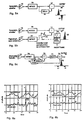
- Figure 5a shows an IF amplifier 10 followed by a detector 70.
- the output of detector 70 is a fluctuating direct current voltage.
- An example of this voltage is shown in the top trace 88 of Figure 6a.
- a subtractor circuit consisting of operational amplifier 87 and delay circuit 83, follows the detector 70 in Figure 5a.
- the delay is set prior to operation and is equal in duration to the length of the received pulse plus the expected length of the largest target. The delay time in this arrangement is not as critical as for the IF subtraction case of Fig. 1.
- An example of the output of operational amplifier 87, which produces a difference signal, is shown as the lower trace 89 in Figure 6a.
- the ideal output is illustrated by pulses 84 and 85 in Figure 5a.
- the second pulse, 85 is either gated out, using conventional circuitry not illustrated, or is ignored by the operator. Occasionally during operation, a signal may appear such as at B in the bottom curve 89 of Figure 6a that could be confused with the real echo. A verification pulse subsequently transmitted by the radar will serve to eliminate such spurious echoes.
- FIG. 5b A somewhat improved arrangement is shown as Figure 5b, though a separate broad beam antenna and receiver are needed.
- the RFI occurring at the time of pulse reception presented at detector 70' is subtracted at differential amplifier 72 from the output of detector 70 to produce output 81 which is illustrated by pulse 86. That output is also illustrated in Figure 6b as trace 91.
- Trace 90 in Figure 6b represents the output of the detector 70 in Figure 6b.
- the delays in the radar antenna channel and in the broad beam antenna channel must be set approximately equal at the time of construction, and there is no need for continual delay adjustment as for the cases of Figure 1. There is a need in most cases for a continual adjustment of the amplitude of the omnidirectional antenna signal.
- This adjustment occurs in the variable amplifier or attenuator 93, which in turn is controlled by the feedback circuit 92, which consists of a switch and sample, integrate, and hold circuits. Radar timing signals, obtained from the associated radar circuitry, not illustrated, controls the sampling time and sampling period. It also controls the resetting of the hold circuits.
- the sign of the voltage out of feedback circuit 92 positive or negative polarity, determines whether the gain of amplifier 93 is increased or decreased.
- This control is such as to force the voltage at 81 to be zero when no radar echo is present.
- the difference output 81 is not sampled by feedback circuit 92.
- a small amount of echo signal will be received by the broad beam antenna, but its power level will typically be 0.01 to 0.00001 as large as the echo signal received by the high gain radar antenna.
- circuit arrangements of Fig. 1 may be modified by replacing each channel with a circuit constructed in accordance with Fig. 5b, whereby the latter circuit is duplicated in number to equal the number of channels in those arrangements. In this case Doppler information is not lost and imaging is possible, and RFI elimination still occurs.
- FIG. 5c A somewhat better arrangement, one not requiring a separate antenna, is illustrated by Figure 5c.
- This arrangement takes samples of the RFI just before and just after the arrival of the desired radar pulse. one half of each of these two samples is subtracted from the output of detector 70 to produce output 82 which is illustrated as pulses 76, 77, and 78. Pulses 77 and 78 are one half the amplitude of pulse 76 and are either time gated out or ignored by the operator.
- the advantage of this scheme is a more accurate sample of RFI at the time of pulse reception than that illustrated by Figure 6a.
- a signal level equal one half the signal level occurring before the echo pulse plus one half the signal level occurring after the echo pulse is subtracted from the signal level at the time of the echo pulse.
- the attenuator 74 reduces the subtract signals by one half, and delays 71 and 75 provide the needed delays.
- these functions can be implemented either in analog fashion or in digital fashion.
- a digital system can also be defined and made to perform the same functions analygous to and as illustrated by the circuits of Figs. 5a, 5b and 5c, previously described.
- the Fourier transformer 56 and adder 63 found in the digital system of Fig. 4, are not needed, so there is just one broadband channel.
- Digital functions handle the processes as illustrated by Figures 5 which were previously described.
Landscapes
- Engineering & Computer Science (AREA)
- Radar, Positioning & Navigation (AREA)
- Remote Sensing (AREA)
- Computer Networks & Wireless Communication (AREA)
- Physics & Mathematics (AREA)
- General Physics & Mathematics (AREA)
- Radar Systems Or Details Thereof (AREA)
Description
Further, the target cannot be imaged. It remains possible to measure target velocity, however, by noting the change in range for successive received pulses. For some radars, such as a search radar, the arrangement illustrated by Figure 6 would be useful and much simpler to implement than the embodiment of Figure 1.
Claims (10)
- Apparatus for transmitting and receiving pulsed RF signals, comprising a transmitter (3) for radiating pulsed RF signals, a directional antenna (7), and a broad band receiver (9) led to said directional antenna (7) for receiving and processing pulsed RF signals of a given frequency in the possible presence of narrow band RFI signals created by a plurality of extraneous narrow band RFI sources, said narrow band RFI being distinct in frequency from one another and from said given frequency, whereby said receiver incidentally detects said RFI signals in addition to detecting pulsed wide band RF signals of said given frequency,
characterized by
separator means (F1, ... Fx) for parsing received signals amongst a plurality of separate and distinct frequency channels in dependence an the frequency of said signals and separately outputting each said channel, whereby a plurality of received RFI signals of different frequencies is produced at the respective channel outputs associated with such frequencies and wherein a received pulsed RF signal is divided into constituent spectral components and said constituent spectral components are individually output from respective channels associated with respective constituent spectral components;
counter signal generating means (29a, ... 29x; 48, 10, F1, 14a, 16a ... 8, 10, Fx, 14x, 16x) for producing a counter signal for each said channel; each said counter signal corresponding to at least a respective RFI signal in a respective one of said plurality of channels, each respective counter signal being of essentially the same amplitude as and phase with said associated respective RFI signal;
first combiner means (27a, ... 27x), responsive to said separator means and to said counter signal generating means, for subtractively combining signals from each of said plurality of channels with the respective ones of said plurality of counter signals from said counter signal generating means to produce a corresponding plurality of difference signals, wherein each said RFI is effectively minimized and wherein the constituent components of a received pulsed RF signal are presented; and
second combiner means (33), coupled to said first combiner means, for summing said plurality of difference signals to provide a composite output signal reproducing said pulsed RF signal. - Apparatus according to claim 1, wherein said counter signal generating means comprises:a plurality of delay means (29a, ... 29x), said plurality corresponding in number to said plurality of channels, and each of said delay means being associated with a corresponding one of said channels, each said delay means being connected to receive the output of the respective channel and output a delayed signal to a corresponding input of said first combiner means (27a, ... 27x), whereby a delayed version of the RFI in the associated channel is supplied to said first combiner means.
- Apparatus according to claim 1 wherein said counter signal generating means comprises:omnidirectional broad beam antenna means (8) for receiving RFI signals propagating from virtually any direction to thereby duplicate RFI signals received by said receiver means;second receiver means (10) for receiving said RFI signals from said omnidirectional broad beam antenna means (8);second separator means (F1, ... Fx) for parsing received signals amongst a plurality of separate and distinct frequency channels and separately outputting each said channel, whereby a plurality of received RFI signals falling within different frequency sub-ranges is produced at the respective channel outputs associated with such frequencies and wherein any received pulsed RF signal is divided into a plurality of constituent spectral components and parsed amongst said plurality of channels; anda plurality of amplitude adjustment means (14a, ... 14x) and delay means, with each of said amplitude adjusting means being serially connected with a corresponding one of said delay means, each of said amplitude adjusting means having an input connected to a respective output of a respective one of said channels defined by said second separator means (F1, ... Fx); and each said delay means having a corresponding output to provide a plurality of outputs of said separator means.
- Apparatus according to any of claims 1 to 3, wherein said separator means comprises a plurality of tuned bandpass filters (F1, ... Fx), each of said tuned bandpass filters having a defined bandwidth and a defined frequency range for selectively passing signals, said defined frequency ranges for said tuned bandpass filters being collectively equal to said predetermined frequency range of said receiver.
- Apparatus according to claim 1 wherein said first combiner means comprises a plurality of combining circuit means (27a, ... 27x), one associated with each said channel of said separator means (F1, ... Fx), for subtractively combining signals from an associated channel with a respective one of said plurality of counter signals from said counter signal generating means (29a, ... 29x; 48, 10, F1, 14a, 16a ... 8, 10, Fx, 14x, 16x), to produce a difference signal, each of said combining circuit means further comprising differential amplifier means (31a, ... 31x).
- Apparatus according to claim 2, wherein each of said delay means ( 29a, ... 29x; 48, 10, F1, 14a, 16a ... 8, 10, Fx, 14x, 16x) is adjustable and each of said delay means includes phase shifting means and further comprises a plurality of automatic adjustment means (47) for adjusting the amount of delay of each of said plurality of delay means of said counter signal generating means to minimize the output of said first combiner means (27a, ... 27x) during the presence of RFI signals at said input to said first combiner means and said counter signal generating means during the absence of a pulse RF signal,
each of said plurality of automatic adjusting means (47), comprising:said switch means (45) being connected between the output of said first combiner means (27) and said compare and logic circuit means (41);sample and hold means (43);switch means (45); andcompare and logic circuit means (41) for analyzing signal levels and for controlling said time delay means of said counter signal generating means;
said sample and hold means (43) closes said switch means (45) during the absence of a pulsed RF signal at said receiver means to provide a sample of the difference signal from said first combiner means (27) to said compare and logic circuit means (41);
said compare and logic circuit means (41) determines from consecutive samples of said difference signal any change in the level of said difference signal and, responsive to determination of an increase in level, adjusts said time delay of said counter signal generating means to produce a decrease in the level of said difference signal, whereby the amount of RFI that can pass through said first combiner means is minimized. - Apparatus according to claim 3, wherein each said delay means is adjustable and further comprises an adjustable phase adjustment circuit (14) and adjustable gain control circuit (16) in series circuit.
- Apparatus according to claim 7, wherein each said delay means is adjustable and further comprises a plurality of automatic adjustment means (47') for adjusting the amount of delay of each of said plurality of delay means of said counter signal generating means to minimize the output of said first combiner means (27) during the presence of RFI signals at said input to said first combiner means during the absence of a pulse RF signal, each of said plurality of automatic adjusting means (47'), comprising:sample and hold means (43');switch means (45');compare and logic circuit means (41') for analyzing signal levels and for controlling said time delay means of said counter signal generating means;said switch means (45') being connected between the output of said first combiner means and said compare and logic circuit means (41');said sample and hold means (43') for closing said switch means (45') during the absence of a pulsed RF signal at said receiver means provides a sample of the difference signal from said first combiner means (27) to said compare and logic circuit means;said compare and logic circuit means (41') determines from consecutive samples of said difference signal any change in the level of said difference signal and, responsive to determination of an increase in level, adjusts said time delay of said counter signal generating means and adjusts said gain to produce a decrease in the level of said difference signal,whereby the amount of RFI that can pass through said first combiner means is minimized; andchopper means (Ch) for alternately coupling the output of said compare and logic circuit means (41') to said phase adjustment circuit (14) and said gain adjustment circuit (16).
- Apparatus according to claim 1, wherein said separator means (F1, ... Fx) comprises:wherein each of said first combiner means (27), counter signal generating means (29) and said second combiner means (33) comprises, respectively, a digital first combiner means (57), a digital counter signal generating means (61) and a digital second combiner means (63).an analog to digital converter (55) for converting signals into digital form;a Fourier transformer (56) responsive to said converter (55) for digitally processing said signal and parsing said digitally processed signal into separate digital channels (F1, ... Fx), each said channel defining a separate frequency range; and
- Method of preventing a plurality of spurious RF sources of different frequencies from producing interference with the detection and processing of desired radar echoes in a wide band pulse radar receiving system capable of receiving such different frequencies, comprising the steps of:separating received signals collectively representing spurious interference signals and the desired radar echo into a plurality of frequency sub-ranges, whereby each spurious signal falls into a respective one of said sub-ranges to produce a separate plurality of spurious signals of individual amplitude and phase together with a component of any desired radar echo that is simultaneously received; generating a counter signal for each separate spurious signal, each said counter signal being equal in amplitude and phase with the amplitude and phase determined from the spurious signal within each respective subrange; subtracting each counter signal from the corresponding spurious signal plus said desired echo component in each said subrange to produce a corresponding difference signal that is essentially a component of the desired radar echo; combining all said difference signals to produce a combined signal in which any interference signals have been minimized, whereby the combined signal represents essentially the desired radar echo.
Priority Applications (1)
| Application Number | Priority Date | Filing Date | Title |
|---|---|---|---|
| EP02006694A EP1225455B1 (en) | 1994-08-10 | 1995-08-09 | Radar apparatus with RFI suppression |
Applications Claiming Priority (3)
| Application Number | Priority Date | Filing Date | Title |
|---|---|---|---|
| US08/288,373 US5473332A (en) | 1994-08-10 | 1994-08-10 | RFI suppression circuit and method |
| US288373 | 1994-08-10 | ||
| PCT/US1995/010401 WO1996008085A2 (en) | 1994-08-10 | 1995-08-09 | Rfi suppression circuit and method |
Related Child Applications (1)
| Application Number | Title | Priority Date | Filing Date |
|---|---|---|---|
| EP02006694A Division EP1225455B1 (en) | 1994-08-10 | 1995-08-09 | Radar apparatus with RFI suppression |
Publications (3)
| Publication Number | Publication Date |
|---|---|
| EP0742908A1 EP0742908A1 (en) | 1996-11-20 |
| EP0742908A4 EP0742908A4 (en) | 1999-05-06 |
| EP0742908B1 true EP0742908B1 (en) | 2003-03-26 |
Family
ID=23106828
Family Applications (2)
| Application Number | Title | Priority Date | Filing Date |
|---|---|---|---|
| EP95943564A Expired - Lifetime EP0742908B1 (en) | 1994-08-10 | 1995-08-09 | Rfi suppression circuit and method |
| EP02006694A Expired - Lifetime EP1225455B1 (en) | 1994-08-10 | 1995-08-09 | Radar apparatus with RFI suppression |
Family Applications After (1)
| Application Number | Title | Priority Date | Filing Date |
|---|---|---|---|
| EP02006694A Expired - Lifetime EP1225455B1 (en) | 1994-08-10 | 1995-08-09 | Radar apparatus with RFI suppression |
Country Status (5)
| Country | Link |
|---|---|
| US (1) | US5473332A (en) |
| EP (2) | EP0742908B1 (en) |
| AU (1) | AU4500496A (en) |
| DE (2) | DE69530069T2 (en) |
| WO (1) | WO1996008085A2 (en) |
Cited By (1)
| Publication number | Priority date | Publication date | Assignee | Title |
|---|---|---|---|---|
| CN102353943A (en) * | 2011-09-29 | 2012-02-15 | 无锡军帅电子科技有限公司 | Method for restraining radio-frequency interference and radar life-detector |
Families Citing this family (31)
| Publication number | Priority date | Publication date | Assignee | Title |
|---|---|---|---|---|
| US6063234A (en) * | 1997-09-10 | 2000-05-16 | Lam Research Corporation | Temperature sensing system for use in a radio frequency environment |
| US5920259A (en) * | 1997-11-10 | 1999-07-06 | Shmuel Hershkovitz | Motion detection with RFI/EMI protection |
| US6052421A (en) * | 1998-09-28 | 2000-04-18 | Northrop Grumman Corporation | Method for separating a desired signal from an interfering signal |
| US6049302A (en) * | 1999-05-04 | 2000-04-11 | Boeing North American | Pulsed doppler radar system with small intermediate frequency filters |
| US6711216B2 (en) * | 2001-06-28 | 2004-03-23 | Intel Corporation | Method and apparatus for an ultra-wideband radio utilizing MEMS filtering |
| EP1580573B1 (en) * | 2002-03-13 | 2006-11-15 | Raytheon Canada Limited | System and method for noise suppression in pre-processed radar data |
| ES2261927T3 (en) * | 2002-03-13 | 2006-11-16 | Raytheon Canada Limited | SYSTEM AND PROCEDURE FOR THE GENERATION OF SPECTERS IN A RADAR. |
| US6891496B2 (en) * | 2002-05-03 | 2005-05-10 | Atheros Communications, Inc. | Method and apparatus for physical layer radar pulse detection and estimation |
| US8190162B2 (en) * | 2003-09-15 | 2012-05-29 | Broadcom Corporation | Radar detection circuit for a WLAN transceiver |
| US7701382B2 (en) * | 2003-09-15 | 2010-04-20 | Broadcom Corporation | Radar detection circuit for a WLAN transceiver |
| EP1528408A1 (en) * | 2003-10-31 | 2005-05-04 | Mitsubishi Electric Information Technology Centre Europe B.V. | Radar system with decomposition of the wideband transmitted signal |
| US7388537B2 (en) * | 2005-10-14 | 2008-06-17 | Escort Inc. | Radar detector with reduced emissions |
| US7864100B2 (en) * | 2007-08-13 | 2011-01-04 | Mcewan Technologies, Llc | Self-referencing radar pulse detector |
| JP5478010B2 (en) * | 2007-11-12 | 2014-04-23 | 株式会社デンソーアイティーラボラトリ | Electronic scanning radar equipment |
| EP2342581B1 (en) * | 2008-09-30 | 2015-02-25 | Intersoft Electronics NV | Clutter reduction in detection systems |
| US20100097266A1 (en) * | 2008-10-21 | 2010-04-22 | Lockheed Martin Corporation | Single platform passive coherent location using a digital receiver |
| US8418211B2 (en) | 2008-12-31 | 2013-04-09 | Echostar Technologies L.L.C. | Antenna diversity for control device applications |
| EP2226615B1 (en) | 2009-03-02 | 2018-08-22 | VEGA Grieshaber KG | Measurement of fill levels by evaluating an echo curve |
| US8907842B1 (en) * | 2009-03-25 | 2014-12-09 | Raytheon Company | Method and apparatus for attenuating a transmitted feedthrough signal |
| JP5284230B2 (en) * | 2009-09-11 | 2013-09-11 | 株式会社東芝 | Weather radar system and its signal processing method |
| US8482364B2 (en) * | 2009-09-13 | 2013-07-09 | International Business Machines Corporation | Differential cross-coupled power combiner or divider |
| DE102010042653A1 (en) * | 2010-10-20 | 2012-04-26 | Robert Bosch Gmbh | Method and device for object detection |
| US8803730B2 (en) * | 2011-07-21 | 2014-08-12 | The Boeing Company | Radar pulse detection using a digital radar receiver |
| US9753131B2 (en) * | 2013-10-09 | 2017-09-05 | Massachusetts Institute Of Technology | Motion tracking via body radio reflections |
| US9239371B1 (en) * | 2013-10-28 | 2016-01-19 | Anritsu Company | High power input protection for signal measurement devices |
| JP6728193B2 (en) * | 2014-10-01 | 2020-07-22 | ジン チョウZHOU, Jin | Circuit and method for transceiver self-interference canceller |
| CN105158741B (en) * | 2015-06-17 | 2018-07-27 | 电子科技大学 | Adaptive anti-interference multipath multi-beam forming method based on matrix reconstruction |
| EP3353569A4 (en) * | 2015-09-21 | 2019-05-01 | Saab AB | Receiver architecture for increased robustness to radar interference |
| US12111419B1 (en) * | 2019-06-25 | 2024-10-08 | Board Of Trustees Of The University Of Alabama, For And On Behalf Of The University Of Alabama In Huntsville | Systems and methods for detecting objects |
| US11474199B2 (en) | 2020-09-03 | 2022-10-18 | Vaisala, Inc. | RFI mitigation in weather radar data |
| WO2023098809A1 (en) * | 2021-12-01 | 2023-06-08 | The University Of Hong Kong | Systems and methods for radio frequency interference suppression in radar |
Family Cites Families (14)
| Publication number | Priority date | Publication date | Assignee | Title |
|---|---|---|---|---|
| US3603996A (en) * | 1968-08-09 | 1971-09-07 | Gen Dynamics Corp | Means and method for detecting doppler signals submerged in clutter |
| US4146889A (en) * | 1972-01-20 | 1979-03-27 | Technology Service Corporation | Method and apparatus for sidelobe reduction in radar |
| US4062011A (en) * | 1972-08-21 | 1977-12-06 | Control Data Corporation | MTI System processor and method |
| US3879729A (en) * | 1973-07-23 | 1975-04-22 | Gen Electric | Moving target indicator with minimum clutter interference |
| US3962704A (en) * | 1974-05-31 | 1976-06-08 | Hughes Aircraft Company | Moving target indicator clutter tracker |
| US5296865A (en) * | 1974-08-23 | 1994-03-22 | The United States Of America As Represented By The Secretary Of The Navy | MTI compatible coherent sidelobe canceller |
| US5162805A (en) * | 1975-02-19 | 1992-11-10 | The United States Of America As Represented By The Secretary Of The Navy | Frequency diversity sidelobe canceller |
| US4153899A (en) * | 1976-03-10 | 1979-05-08 | Westinghouse Electric Corp. | MTI radar system and method |
| US4122448A (en) * | 1977-07-21 | 1978-10-24 | Westinghouse Electric Corp. | Automatic phase and gain balance controller for a baseband processor |
| DE3028225C1 (en) * | 1980-07-25 | 1992-09-17 | Siemens Ag | Radar receiver |
| FR2505052A1 (en) * | 1981-04-30 | 1982-11-05 | Thomson Csf | METHOD AND DEVICE FOR REDUCING THE POWER OF THE INTERFERENCE SIGNALS RECEIVED BY THE SECONDARY LOBES OF A RADAR ANTENNA |
| US4617570A (en) * | 1983-08-26 | 1986-10-14 | Gutleber Frank S | Interference cancelling receiver having high angular resolution intercept of transmitted radiators |
| US4622552A (en) * | 1984-01-31 | 1986-11-11 | The United States Of America As Represented By The Secretary Of The Navy | Factored matched filter/FFT radar Doppler processor |
| US5212490A (en) * | 1991-06-16 | 1993-05-18 | Hydroacoustics, Inc. | Echo ranging system for detecting velocity and range of targets using composite doppler invariant-like transmissions with suppression of false targets |
-
1994
- 1994-08-10 US US08/288,373 patent/US5473332A/en not_active Expired - Lifetime
-
1995
- 1995-08-09 EP EP95943564A patent/EP0742908B1/en not_active Expired - Lifetime
- 1995-08-09 AU AU45004/96A patent/AU4500496A/en not_active Abandoned
- 1995-08-09 DE DE69530069T patent/DE69530069T2/en not_active Expired - Lifetime
- 1995-08-09 WO PCT/US1995/010401 patent/WO1996008085A2/en not_active Ceased
- 1995-08-09 EP EP02006694A patent/EP1225455B1/en not_active Expired - Lifetime
- 1995-08-09 DE DE69533738T patent/DE69533738T2/en not_active Expired - Lifetime
Cited By (2)
| Publication number | Priority date | Publication date | Assignee | Title |
|---|---|---|---|---|
| CN102353943A (en) * | 2011-09-29 | 2012-02-15 | 无锡军帅电子科技有限公司 | Method for restraining radio-frequency interference and radar life-detector |
| CN102353943B (en) * | 2011-09-29 | 2015-07-22 | 无锡军帅电子科技有限公司 | Method for restraining radio-frequency interference and radar life-detector |
Also Published As
| Publication number | Publication date |
|---|---|
| WO1996008085A3 (en) | 1996-05-17 |
| EP0742908A4 (en) | 1999-05-06 |
| EP1225455A2 (en) | 2002-07-24 |
| DE69533738D1 (en) | 2004-12-09 |
| DE69530069D1 (en) | 2003-04-30 |
| DE69533738T2 (en) | 2005-10-27 |
| AU4500496A (en) | 1996-03-27 |
| US5473332A (en) | 1995-12-05 |
| EP0742908A1 (en) | 1996-11-20 |
| EP1225455B1 (en) | 2004-11-03 |
| EP1225455A3 (en) | 2003-05-21 |
| WO1996008085A2 (en) | 1996-03-14 |
| DE69530069T2 (en) | 2003-11-06 |
Similar Documents
| Publication | Publication Date | Title |
|---|---|---|
| US5473332A (en) | RFI suppression circuit and method | |
| WO1996008085A9 (en) | Rfi suppression circuit and method | |
| US3202990A (en) | Intermediate frequency side-lobe canceller | |
| JP2815208B2 (en) | Adaptive waveform radar | |
| Saini et al. | DTV signal ambiguity function analysis for radar application | |
| US7202812B2 (en) | Technique for compensation of transmit leakage in radar receiver | |
| US4628318A (en) | Ground clutter suppression technique | |
| US5483680A (en) | Tuning method for automatic antenna couplers | |
| US4313116A (en) | Hybrid adaptive sidelobe canceling system | |
| US20100302091A1 (en) | Wideband interference cancellation using dsp algorithms | |
| US5237332A (en) | Receiver distortion correction circuit and method | |
| US5200753A (en) | Monopulse radar jammer using millimeter wave techniques | |
| US6727840B1 (en) | Interference suppression circuit and method thereof for multi-channel receivers | |
| US5361074A (en) | Mainlobe canceller system | |
| KR100734031B1 (en) | Intermodulation Effect Cancellation Circuit and Method | |
| US20050122256A1 (en) | Signal analysis | |
| US4714927A (en) | Pulse doppler radar with variable pulse repetition rate | |
| US6653969B1 (en) | Dispersive jammer cancellation | |
| GB2221545A (en) | Simultaneous signal frequency measurement | |
| US7295145B2 (en) | Selective-sampling receiver | |
| GB2259209A (en) | Radar receivers | |
| US5101210A (en) | Signal dynamic range compression apparatus and method including clutter estimation and reduction | |
| GB2318237A (en) | Pulse doppler radar device with elimination of jammer by neutralization | |
| US6181744B1 (en) | Method and system for improving process shadow time within a pulsed signal processing system | |
| US5418540A (en) | Method and apparatus for eliminating signal sidelobes from a received signal frame in a multichannel receiver |
Legal Events
| Date | Code | Title | Description |
|---|---|---|---|
| PUAI | Public reference made under article 153(3) epc to a published international application that has entered the european phase |
Free format text: ORIGINAL CODE: 0009012 |
|
| 17P | Request for examination filed |
Effective date: 19960403 |
|
| AK | Designated contracting states |
Kind code of ref document: A1 Designated state(s): DE FR GB |
|
| A4 | Supplementary search report drawn up and despatched |
Effective date: 19990324 |
|
| AK | Designated contracting states |
Kind code of ref document: A4 Designated state(s): DE FR GB |
|
| 17Q | First examination report despatched |
Effective date: 20001003 |
|
| GRAH | Despatch of communication of intention to grant a patent |
Free format text: ORIGINAL CODE: EPIDOS IGRA |
|
| GRAH | Despatch of communication of intention to grant a patent |
Free format text: ORIGINAL CODE: EPIDOS IGRA |
|
| GRAA | (expected) grant |
Free format text: ORIGINAL CODE: 0009210 |
|
| AK | Designated contracting states |
Designated state(s): DE FR GB |
|
| REG | Reference to a national code |
Ref country code: GB Ref legal event code: FG4D |
|
| REF | Corresponds to: |
Ref document number: 69530069 Country of ref document: DE Date of ref document: 20030430 Kind code of ref document: P |
|
| ET | Fr: translation filed | ||
| PLBE | No opposition filed within time limit |
Free format text: ORIGINAL CODE: 0009261 |
|
| STAA | Information on the status of an ep patent application or granted ep patent |
Free format text: STATUS: NO OPPOSITION FILED WITHIN TIME LIMIT |
|
| 26N | No opposition filed |
Effective date: 20031230 |
|
| PGFP | Annual fee paid to national office [announced via postgrant information from national office to epo] |
Ref country code: DE Payment date: 20140827 Year of fee payment: 20 |
|
| PGFP | Annual fee paid to national office [announced via postgrant information from national office to epo] |
Ref country code: GB Payment date: 20140827 Year of fee payment: 20 Ref country code: FR Payment date: 20140818 Year of fee payment: 20 |
|
| REG | Reference to a national code |
Ref country code: DE Ref legal event code: R071 Ref document number: 69530069 Country of ref document: DE |
|
| REG | Reference to a national code |
Ref country code: GB Ref legal event code: PE20 Expiry date: 20150808 |
|
| PG25 | Lapsed in a contracting state [announced via postgrant information from national office to epo] |
Ref country code: GB Free format text: LAPSE BECAUSE OF EXPIRATION OF PROTECTION Effective date: 20150808 |