EP0742567B1 - Capacitive and inductive element - Google Patents
Capacitive and inductive element Download PDFInfo
- Publication number
- EP0742567B1 EP0742567B1 EP96107396A EP96107396A EP0742567B1 EP 0742567 B1 EP0742567 B1 EP 0742567B1 EP 96107396 A EP96107396 A EP 96107396A EP 96107396 A EP96107396 A EP 96107396A EP 0742567 B1 EP0742567 B1 EP 0742567B1
- Authority
- EP
- European Patent Office
- Prior art keywords
- plates
- element according
- capacitive
- core
- circuit
- Prior art date
- Legal status (The legal status is an assumption and is not a legal conclusion. Google has not performed a legal analysis and makes no representation as to the accuracy of the status listed.)
- Expired - Lifetime
Links
- 230000001939 inductive effect Effects 0.000 title claims description 20
- 230000005291 magnetic effect Effects 0.000 claims description 18
- 238000004804 winding Methods 0.000 claims description 12
- 239000004020 conductor Substances 0.000 claims description 6
- 239000003989 dielectric material Substances 0.000 claims description 3
- 239000003302 ferromagnetic material Substances 0.000 claims description 3
- 239000003990 capacitor Substances 0.000 description 13
- 208000028659 discharge Diseases 0.000 description 6
- 239000002184 metal Substances 0.000 description 3
- 230000003071 parasitic effect Effects 0.000 description 3
- 229920002799 BoPET Polymers 0.000 description 2
- 239000005041 Mylar™ Substances 0.000 description 2
- 238000010586 diagram Methods 0.000 description 2
- 239000011810 insulating material Substances 0.000 description 2
- ATJFFYVFTNAWJD-UHFFFAOYSA-N Tin Chemical compound [Sn] ATJFFYVFTNAWJD-UHFFFAOYSA-N 0.000 description 1
- 230000008878 coupling Effects 0.000 description 1
- 238000010168 coupling process Methods 0.000 description 1
- 238000005859 coupling reaction Methods 0.000 description 1
- 230000000694 effects Effects 0.000 description 1
- 230000005670 electromagnetic radiation Effects 0.000 description 1
- 238000000034 method Methods 0.000 description 1
- 238000007789 sealing Methods 0.000 description 1
- 238000003466 welding Methods 0.000 description 1
Images

Classifications
-
- H—ELECTRICITY
- H01—ELECTRIC ELEMENTS
- H01G—CAPACITORS; CAPACITORS, RECTIFIERS, DETECTORS, SWITCHING DEVICES, LIGHT-SENSITIVE OR TEMPERATURE-SENSITIVE DEVICES OF THE ELECTROLYTIC TYPE
- H01G4/00—Fixed capacitors; Processes of their manufacture
- H01G4/40—Structural combinations of fixed capacitors with other electric elements, the structure mainly consisting of a capacitor, e.g. RC combinations
-
- H—ELECTRICITY
- H01—ELECTRIC ELEMENTS
- H01J—ELECTRIC DISCHARGE TUBES OR DISCHARGE LAMPS
- H01J2229/00—Details of cathode ray tubes or electron beam tubes
- H01J2229/58—Electron beam control inside the vessel
- H01J2229/581—Electron beam control inside the vessel by magnetic means
-
- H—ELECTRICITY
- H01—ELECTRIC ELEMENTS
- H01J—ELECTRIC DISCHARGE TUBES OR DISCHARGE LAMPS
- H01J2229/00—Details of cathode ray tubes or electron beam tubes
- H01J2229/58—Electron beam control inside the vessel
- H01J2229/583—Electron beam control inside the vessel at the source
- H01J2229/5835—Electron beam control inside the vessel at the source cooperating with the electron gun
Definitions
- the present invention relates to a capacitive and inductive element.
- capacitors are formed from two metal plates separated by a dielectric.
- shape and parameters of the capacitor are designed in such a way as to eliminate or at least reduce undesired associated inductance and/or resistance effects due to the imperfection of the physical components.
- inductors used at present are made from coils and are optimized in such a way as to eliminate undesired parasitic effects.
- circuits in which both capacitive and inductive characteristics are required, and in which both capacitors and inductors are therefore provided separately. This results in significantly large dimensions and complexity, which is a disadvantage in certain applications in view of the current trend towards the reduction of the dimensions of electrical circuits.
- DE-A-3909528 discloses a capacitive and inductive element comprising one pair of plates formed by sheets of conductive material wound around a magnetic core of ferromagnetic material and separated from each other by dielectric material.
- the object of the present invention is to provide a component having controlled characteristics which are both capacitive and inductive and which, in particular, is straightforward and cheap to implement.
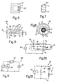
- FIGS 1 and 2 show an embodiment of the capacitive and inductive element 1 according to the invention.
- the element 1 comprises a pair of plates 2 and 3 formed by two conductive leaves or sheets (typically made of metal) wound in a spiral around a core 4 of ferromagnetic material and separated from each other and from the core 4 by a dielectric 5.
- the plates 2 and 3 have ends (corresponding to the ends of the two spirals visible in the view from above) forming terminals A, C and D, B respectively.
- the element 1 has an equivalent circuit shown in Fig. 5, in which the terminals A-D correspond to the terminals A-D in Figs. 1 and 2.
- the circuit 7, of the type with distributed constants comprises a plurality of capacitive elements dC interposed between the line delimited by the terminals A and C and the line delimited by the terminals D and B and a plurality of inductive elements dL arranged along the said lines A-C and D-B.
- the inductive elements dL are coupled together magnetically.
- FIG. 3 Simplified equivalent circuits of the circuit 7 with distributed constants as shown in Fig. 5 are shown in Figs. 3 and 4 and relate to the cases of circuits with two terminals and four terminals respectively.
- the circuit 8 shown in Fig. 3 has two terminals A and B, corresponding to the terminals A, B of the element 1, between which are arranged an inductor 10 and a capacitor 11, connected together in series.
- the circuit 15 shown in Fig. 4 has four terminals A-D, similar to the corresponding terminals of Figs. 1 and 2; an inductor 16 is arranged between the terminals A and C; a capacitor 17 is arranged between the terminals A and D; a capacitor 18 is arranged between the terminals C and B, and an inductor 19 is arranged between the terminals D and B.
- the capacitive surfaces may be insulated from each other by any dielectric material suitable for the purpose.
- the element 1 is made by winding two sheets of insulating material (for example mylar), metal-coated on one side, in a spiral around the core 4.
- insulating material for example mylar
- the magnetic circuit of the element 1 may be open or closed, according to the shape of the core 4; in particular, Fig. 6 shows a typical core 21 of square shape, around one side of which are wound the plates 2 and 3 of the capacitor, shown diagrammatically in the figure as a conductor 22, forming a closed magnetic circuit. Conversely, Fig. 7 shows a magnetic core 23 of cylindrical shape, similar to that shown in Figs. 1 and 2, forming an open magnetic circuit.
- the magnetic core may, however, have any shape suitable for forming a closed or open circuit, for example the conventional "core pot", a coupled pair of cylindrical magnetic cores, a single C-shaped core, etc.
- the magnetic circuit may be connected to other windings of the type shown, in other words formed by wound plates, or of a conventional (wire) type, thus forming a transformer with capacitive and inductive characteristics.
- a transformer element 24 of such a type, with a conventional winding around the core is shown, for example, in Fig. 8, in which a wire winding 25 is arranged around the core 4, and the plates 2, 3 are arranged around the wire winding.
- FIG. 9 shows the flat unwound plates of a capacitive and inductive element 26, also comprising a magnetic core 4 which is not shown.
- This element 26 comprises a plurality of first plates 27', 27", 27'", and a plurality of second plates 28', 28", 28'".
- the first plates 27 are arranged side by side but separated from each other and are connected together along a first end which forms a terminal A' similar to the terminal A shown in Fig. 1 (comb structure).
- the second plates 28 also form a comb structure, being connected together electrically along an end which forms a terminal B' similar to the terminal B shown in Fig. 1.
- the plates 27, 28 are arranged so that they are interposed with each other in an interdigitated configuration, in other words in such a way that each second plate 28 is arranged between a pair of adjacent first plates 27.
- the unconnected ends C', C", C'" of the first plates 27 and the unconnected ends D', D", D'" of the second plates form auxiliary terminals.
- the solution shown in Fig. 9 enables the capacitive component between the terminals A' and B' to be increased independently of the number of wound turns in each element 26.
- the capacitive and inductive element described has the following advantages. In the first place, it enables the number of components in the circuits having an equivalent circuit similar to those shown in Figs. 3-5 to be minimized, thus reducing the overall dimensions. Moreover, in the case of application to high-voltage circuits, the fact that the same insulating method is used for the capacitor and the inductor is advantageous, reducing the associated costs.
- the external connections can be reduced; consequently, in circuits in which high-frequency voltage and/or current components are present, the electromagnetic radiation is reduced and, in circuits in which high currents are present, the efficiency is improved. In high-voltage circuits, the reduction of the external connections also enables the efficiency to be improved and reduces the risk of discharges at the external connections.
- the element described may be used as a discrete element in series L/C circuits of the type illustrated in Figs. 3-5, in resonant L/C circuits, or in resonant positive boosters, for example for starting discharge lamps.
- the positive booster 29 shown in Fig. 10 comprises an alternating voltage generator 30 to which a resonant circuit 15, identical to that shown in Fig. 4 (and formed by the capacitive and inductive element 1), and a lamp 31 are connected in parallel.
- the resonant circuit 15, comprising the inductors 16, 19 and the capacitors 17, 18, is designed to resonate at the frequency of the alternating voltage v in the absence of a load (the lamp 31).
- the load the discharge lamp 31
- the circuit ceases to resonate and the system may be shown schematically as in Fig.
- the circuit 15 is replaced by two impedances 33, 34 with values Z 1 and Z 2 , arranged between terminals A and C and terminals A and D respectively.
- the impedance Z 1 may be very low, and the impedance Z 2 may be very high.
- the circuit 29 can generate the high voltage necessary to start the discharge lamp 31 before the lamp is connected, but has a lower series impedance during the operation of the lamp after starting, as required, using only the component 1 for the circuit 15.
- the capacitive and inductive element 1 can also be used to generate pulsed magnetic fields in the magnetic circuit, using the initial charging of the capacitor 11 (equivalent circuit 8 in Fig. 2) and its subsequent discharge.
- An example of the application of a circuit 38 for generating pulsed magnetic fields is shown in Fig. 12, in which the capacitive and inductive element 1 according to the invention is shown diagrammatically with the circuit 8 of Fig. 2 and is connected in parallel to a switch 39 and to a continuous voltage generator 40.
- the capacitor 11 is initially charged (with the switch 39 open) at the voltage v by means of the generator 40.
- the switch 39 When the switch 39 is closed, the capacitor 11 discharges through the inductor 10, causing a high current peak and consequently a pulsed magnetic field in the core (4 in Fig. 1) of the inductor 10.
- the circuit shown may therefore be used advantageously in machines for magnetizing permanent magnets, in machines for magnetic forming and in welding machines, by coupling the magnetic circuit to a secondary (for example the winding 25 in Fig. 8).
Landscapes
- Engineering & Computer Science (AREA)
- Power Engineering (AREA)
- Manufacturing & Machinery (AREA)
- Microelectronics & Electronic Packaging (AREA)
- Coils Or Transformers For Communication (AREA)
- Coils Of Transformers For General Uses (AREA)
- Near-Field Transmission Systems (AREA)
Description
Claims (11)
- Capacitive and inductive element (1) comprising at least one pair of plates (2, 3) formed by sheets of conductive material wound around a magnetic core (4) of ferromagnetic material and separated from each other by dielectric material (5); characterized in further comprising a plurality of first plates (27', 27", 27'") connected together at one end and a plurality of second plates (28', 28", 28'") connected together at one of their ends, each of said second plates extending between an adjacent pair of first plates, and said first and second plates being wound in a spiral around said core.
- Capacitive and inductive element according to Claim 1, wherein said plates (2, 3) are wound in a spiral, one around the other.
- Element according to Claim 1 or 2, wherein said core (21) has a closed shape.
- Element according to Claim 1 or 2, wherein said core (23) has an open shape.
- Element according to any of the preceding claims, wherein it comprises a winding (25) of conductive material extending around said magnetic core (4).
- Element according to Claim 5, wherein said winding is of the wire type.
- Element according to Claim 5, wherein said winding (25) comprises a further sheet of conductive material.
- Element according to any of the preceding claims, wherein it forms a series LC circuit (8).
- Element according to any of the preceding claims, wherein it forms a resonant LC circuit (15).
- Element according to any of the preceding claims, and forming an oscillating positive booster (29) connected between an alternating voltage generator (30) and a load (31).
- Element according to any of the preceding claims, and forming a generator of pulsed magnetic fields (38) connected in parallel to a continuous voltage generator (40) and to a switch (39).
Applications Claiming Priority (2)
| Application Number | Priority Date | Filing Date | Title |
|---|---|---|---|
| IT95TO000382A IT1279205B1 (en) | 1995-05-12 | 1995-05-12 | CAPACITIVE-INDUCTIVE ELEMENT |
| ITTO950382 | 1995-05-12 |
Publications (2)
| Publication Number | Publication Date |
|---|---|
| EP0742567A1 EP0742567A1 (en) | 1996-11-13 |
| EP0742567B1 true EP0742567B1 (en) | 2002-12-11 |
Family
ID=11413553
Family Applications (1)
| Application Number | Title | Priority Date | Filing Date |
|---|---|---|---|
| EP96107396A Expired - Lifetime EP0742567B1 (en) | 1995-05-12 | 1996-05-09 | Capacitive and inductive element |
Country Status (5)
| Country | Link |
|---|---|
| EP (1) | EP0742567B1 (en) |
| BR (1) | BR9601667A (en) |
| DE (1) | DE69625273T2 (en) |
| ES (1) | ES2188689T3 (en) |
| IT (1) | IT1279205B1 (en) |
Families Citing this family (1)
| Publication number | Priority date | Publication date | Assignee | Title |
|---|---|---|---|---|
| CN100378877C (en) | 1998-03-13 | 2008-04-02 | 松下电器产业株式会社 | Composite element and its manufacturing method |
Family Cites Families (2)
| Publication number | Priority date | Publication date | Assignee | Title |
|---|---|---|---|---|
| US4788624A (en) * | 1987-12-21 | 1988-11-29 | North American Philips Corporation | Capacitor having current surge protection |
| DE3909528A1 (en) * | 1988-03-23 | 1989-10-12 | Murata Manufacturing Co | IMPACT FILTER |
-
1995
- 1995-05-12 IT IT95TO000382A patent/IT1279205B1/en active IP Right Grant
-
1996
- 1996-05-09 DE DE69625273T patent/DE69625273T2/en not_active Expired - Fee Related
- 1996-05-09 ES ES96107396T patent/ES2188689T3/en not_active Expired - Lifetime
- 1996-05-09 EP EP96107396A patent/EP0742567B1/en not_active Expired - Lifetime
- 1996-05-13 BR BR9601667A patent/BR9601667A/en not_active Application Discontinuation
Also Published As
| Publication number | Publication date |
|---|---|
| ITTO950382A1 (en) | 1996-11-12 |
| IT1279205B1 (en) | 1997-12-04 |
| DE69625273D1 (en) | 2003-01-23 |
| EP0742567A1 (en) | 1996-11-13 |
| ITTO950382A0 (en) | 1995-05-12 |
| DE69625273T2 (en) | 2003-08-28 |
| BR9601667A (en) | 1998-03-31 |
| ES2188689T3 (en) | 2003-07-01 |
Similar Documents
| Publication | Publication Date | Title |
|---|---|---|
| CN101454957A (en) | Contactless Energy Transfer System | |
| US6529363B2 (en) | Capacitor integrated into transformer by multi-layer foil winding | |
| EP0597661A1 (en) | Improvements in or relating to an electrical arrangement | |
| US3704390A (en) | Combined capacitor-inductor reactor device having transformer characteristics | |
| WO2005122193A1 (en) | Planar high voltage transformer device | |
| US6278355B1 (en) | Transformer winding | |
| EP0742567A1 (en) | Capacitive and inductive element | |
| US7113066B2 (en) | Electronic inductive and capacitive component | |
| JP3703434B2 (en) | High voltage pulse transformer | |
| EP3607636B1 (en) | A system for wireless power transfer between low and high electrical potential, and a high voltage circuit breaker | |
| KR102554936B1 (en) | Planar transformer | |
| CN110945784A (en) | Inductor-capacitor filters and associated systems and methods | |
| JPH06132147A (en) | Step-up transformer | |
| US20240395455A1 (en) | Elecromagnetic component with reduced parasitic capacitance induced loss | |
| Duong et al. | Analysis of series-connected double-layer coils for MHz inductive power transfer | |
| JPH04285475A (en) | Power source | |
| US6320316B1 (en) | Apparatus for coupling power into a body of gas | |
| GB2263362A (en) | Radio interference suppression device | |
| SU1073808A1 (en) | High-frequency transformer | |
| SU757116A1 (en) | LINEAR INDUCTION ACCELERATOR | |
| SU1683082A1 (en) | Inductive device | |
| JPH0341707A (en) | Pulse transformer | |
| JPH04352304A (en) | Pulse transformer and high voltage pulse generator | |
| JPH07211549A (en) | Electromagnetic equipment | |
| GB2350239A (en) | Magnetic circuit laminations forming a capacitor |
Legal Events
| Date | Code | Title | Description |
|---|---|---|---|
| PUAI | Public reference made under article 153(3) epc to a published international application that has entered the european phase |
Free format text: ORIGINAL CODE: 0009012 |
|
| AK | Designated contracting states |
Kind code of ref document: A1 Designated state(s): DE ES FR GB SE |
|
| 17P | Request for examination filed |
Effective date: 19961116 |
|
| 17Q | First examination report despatched |
Effective date: 20010703 |
|
| GRAG | Despatch of communication of intention to grant |
Free format text: ORIGINAL CODE: EPIDOS AGRA |
|
| GRAG | Despatch of communication of intention to grant |
Free format text: ORIGINAL CODE: EPIDOS AGRA |
|
| GRAH | Despatch of communication of intention to grant a patent |
Free format text: ORIGINAL CODE: EPIDOS IGRA |
|
| RAP1 | Party data changed (applicant data changed or rights of an application transferred) |
Owner name: MAGNETI MARELLI POWERTRAIN S.P.A. |
|
| GRAH | Despatch of communication of intention to grant a patent |
Free format text: ORIGINAL CODE: EPIDOS IGRA |
|
| GRAA | (expected) grant |
Free format text: ORIGINAL CODE: 0009210 |
|
| AK | Designated contracting states |
Kind code of ref document: B1 Designated state(s): DE ES FR GB SE |
|
| REG | Reference to a national code |
Ref country code: GB Ref legal event code: FG4D |
|
| REF | Corresponds to: |
Ref document number: 69625273 Country of ref document: DE Date of ref document: 20030123 |
|
| REG | Reference to a national code |
Ref country code: ES Ref legal event code: FG2A Ref document number: 2188689 Country of ref document: ES Kind code of ref document: T3 |
|
| ET | Fr: translation filed | ||
| PLBE | No opposition filed within time limit |
Free format text: ORIGINAL CODE: 0009261 |
|
| STAA | Information on the status of an ep patent application or granted ep patent |
Free format text: STATUS: NO OPPOSITION FILED WITHIN TIME LIMIT |
|
| 26N | No opposition filed |
Effective date: 20030912 |
|
| PGFP | Annual fee paid to national office [announced via postgrant information from national office to epo] |
Ref country code: FR Payment date: 20050428 Year of fee payment: 10 |
|
| PGFP | Annual fee paid to national office [announced via postgrant information from national office to epo] |
Ref country code: GB Payment date: 20050504 Year of fee payment: 10 |
|
| PGFP | Annual fee paid to national office [announced via postgrant information from national office to epo] |
Ref country code: SE Payment date: 20050516 Year of fee payment: 10 Ref country code: ES Payment date: 20050516 Year of fee payment: 10 |
|
| PGFP | Annual fee paid to national office [announced via postgrant information from national office to epo] |
Ref country code: DE Payment date: 20050725 Year of fee payment: 10 |
|
| PG25 | Lapsed in a contracting state [announced via postgrant information from national office to epo] |
Ref country code: GB Free format text: LAPSE BECAUSE OF NON-PAYMENT OF DUE FEES Effective date: 20060509 |
|
| PG25 | Lapsed in a contracting state [announced via postgrant information from national office to epo] |
Ref country code: SE Free format text: LAPSE BECAUSE OF NON-PAYMENT OF DUE FEES Effective date: 20060510 Ref country code: ES Free format text: LAPSE BECAUSE OF NON-PAYMENT OF DUE FEES Effective date: 20060510 |
|
| PG25 | Lapsed in a contracting state [announced via postgrant information from national office to epo] |
Ref country code: DE Free format text: LAPSE BECAUSE OF NON-PAYMENT OF DUE FEES Effective date: 20061201 |
|
| EUG | Se: european patent has lapsed | ||
| GBPC | Gb: european patent ceased through non-payment of renewal fee |
Effective date: 20060509 |
|
| REG | Reference to a national code |
Ref country code: FR Ref legal event code: ST Effective date: 20070131 |
|
| REG | Reference to a national code |
Ref country code: ES Ref legal event code: FD2A Effective date: 20060510 |
|
| PG25 | Lapsed in a contracting state [announced via postgrant information from national office to epo] |
Ref country code: FR Free format text: LAPSE BECAUSE OF NON-PAYMENT OF DUE FEES Effective date: 20060531 |