EP0738185B1 - Spin-on-glass process with controlled environment - Google Patents
Spin-on-glass process with controlled environment Download PDFInfo
- Publication number
- EP0738185B1 EP0738185B1 EP95901797A EP95901797A EP0738185B1 EP 0738185 B1 EP0738185 B1 EP 0738185B1 EP 95901797 A EP95901797 A EP 95901797A EP 95901797 A EP95901797 A EP 95901797A EP 0738185 B1 EP0738185 B1 EP 0738185B1
- Authority
- EP
- European Patent Office
- Prior art keywords
- integrated circuit
- spinning
- controlling
- spin
- controllable environment
- Prior art date
- Legal status (The legal status is an assumption and is not a legal conclusion. Google has not performed a legal analysis and makes no representation as to the accuracy of the status listed.)
- Expired - Lifetime
Links
Images


Classifications
-
- B—PERFORMING OPERATIONS; TRANSPORTING
- B05—SPRAYING OR ATOMISING IN GENERAL; APPLYING FLUENT MATERIALS TO SURFACES, IN GENERAL
- B05C—APPARATUS FOR APPLYING FLUENT MATERIALS TO SURFACES, IN GENERAL
- B05C11/00—Component parts, details or accessories not specifically provided for in groups B05C1/00 - B05C9/00
- B05C11/02—Apparatus for spreading or distributing liquids or other fluent materials already applied to a surface ; Controlling means therefor; Control of the thickness of a coating by spreading or distributing liquids or other fluent materials already applied to the coated surface
- B05C11/08—Spreading liquid or other fluent material by manipulating the work, e.g. tilting
-
- B—PERFORMING OPERATIONS; TRANSPORTING
- B05—SPRAYING OR ATOMISING IN GENERAL; APPLYING FLUENT MATERIALS TO SURFACES, IN GENERAL
- B05D—PROCESSES FOR APPLYING FLUENT MATERIALS TO SURFACES, IN GENERAL
- B05D1/00—Processes for applying liquids or other fluent materials
- B05D1/002—Processes for applying liquids or other fluent materials the substrate being rotated
- B05D1/005—Spin coating
-
- H—ELECTRICITY
- H10—SEMICONDUCTOR DEVICES; ELECTRIC SOLID-STATE DEVICES NOT OTHERWISE PROVIDED FOR
- H10P—GENERIC PROCESSES OR APPARATUS FOR THE MANUFACTURE OR TREATMENT OF DEVICES COVERED BY CLASS H10
- H10P14/00—Formation of materials, e.g. in the shape of layers or pillars
- H10P14/60—Formation of materials, e.g. in the shape of layers or pillars of insulating materials
- H10P14/63—Formation of materials, e.g. in the shape of layers or pillars of insulating materials characterised by the formation processes
- H10P14/6326—Deposition processes
- H10P14/6328—Deposition from the gas or vapour phase
- H10P14/6334—Deposition from the gas or vapour phase using decomposition or reaction of gaseous or vapour phase compounds, i.e. chemical vapour deposition
- H10P14/6336—Deposition from the gas or vapour phase using decomposition or reaction of gaseous or vapour phase compounds, i.e. chemical vapour deposition in the presence of a plasma [PECVD]
-
- H—ELECTRICITY
- H10—SEMICONDUCTOR DEVICES; ELECTRIC SOLID-STATE DEVICES NOT OTHERWISE PROVIDED FOR
- H10P—GENERIC PROCESSES OR APPARATUS FOR THE MANUFACTURE OR TREATMENT OF DEVICES COVERED BY CLASS H10
- H10P14/00—Formation of materials, e.g. in the shape of layers or pillars
- H10P14/60—Formation of materials, e.g. in the shape of layers or pillars of insulating materials
- H10P14/63—Formation of materials, e.g. in the shape of layers or pillars of insulating materials characterised by the formation processes
- H10P14/6326—Deposition processes
- H10P14/6342—Liquid deposition, e.g. spin-coating, sol-gel techniques or spray coating
-
- H—ELECTRICITY
- H10—SEMICONDUCTOR DEVICES; ELECTRIC SOLID-STATE DEVICES NOT OTHERWISE PROVIDED FOR
- H10P—GENERIC PROCESSES OR APPARATUS FOR THE MANUFACTURE OR TREATMENT OF DEVICES COVERED BY CLASS H10
- H10P14/00—Formation of materials, e.g. in the shape of layers or pillars
- H10P14/60—Formation of materials, e.g. in the shape of layers or pillars of insulating materials
- H10P14/66—Formation of materials, e.g. in the shape of layers or pillars of insulating materials characterised by the type of materials
- H10P14/668—Formation of materials, e.g. in the shape of layers or pillars of insulating materials characterised by the type of materials the materials being characterised by the deposition precursor materials
- H10P14/6681—Formation of materials, e.g. in the shape of layers or pillars of insulating materials characterised by the type of materials the materials being characterised by the deposition precursor materials the precursor containing a compound comprising Si
- H10P14/6684—Formation of materials, e.g. in the shape of layers or pillars of insulating materials characterised by the type of materials the materials being characterised by the deposition precursor materials the precursor containing a compound comprising Si the compound comprising silicon and oxygen
- H10P14/6686—Formation of materials, e.g. in the shape of layers or pillars of insulating materials characterised by the type of materials the materials being characterised by the deposition precursor materials the precursor containing a compound comprising Si the compound comprising silicon and oxygen the compound being a molecule comprising at least one silicon-oxygen bond and the compound having hydrogen or an organic group attached to the silicon or oxygen, e.g. a siloxane
-
- H—ELECTRICITY
- H10—SEMICONDUCTOR DEVICES; ELECTRIC SOLID-STATE DEVICES NOT OTHERWISE PROVIDED FOR
- H10P—GENERIC PROCESSES OR APPARATUS FOR THE MANUFACTURE OR TREATMENT OF DEVICES COVERED BY CLASS H10
- H10P14/00—Formation of materials, e.g. in the shape of layers or pillars
- H10P14/60—Formation of materials, e.g. in the shape of layers or pillars of insulating materials
- H10P14/69—Inorganic materials
- H10P14/692—Inorganic materials composed of oxides, glassy oxides or oxide-based glasses
- H10P14/6921—Inorganic materials composed of oxides, glassy oxides or oxide-based glasses containing silicon
- H10P14/6922—Inorganic materials composed of oxides, glassy oxides or oxide-based glasses containing silicon the material containing Si, O and at least one of H, N, C, F or other non-metal elements, e.g. SiOC, SiOC:H or SiONC
- H10P14/6927—Inorganic materials composed of oxides, glassy oxides or oxide-based glasses containing silicon the material containing Si, O and at least one of H, N, C, F or other non-metal elements, e.g. SiOC, SiOC:H or SiONC the material being a silicon oxynitride, e.g. SiON or SiON:H
Definitions
- the present invention relates to planarization processes used during integrated circuit manufacturing; and more particularly to an improved spin-on-glass process in which the environment is controlled during the spread/flow-in step and other steps of the process.
- SOG Spin-on-glass
- a high degree of planarity on the wafer surface is needed for fine photolithographic resolution.
- planarity is needed to avoid metal stringers after etching of the metal lines which might be left in impressions on the surface of the wafer and cause shorts on the device.
- VLSI Multilevel Interconnection Conferences such as Ting, et al., "Planarization Process Using Spin-On-Glass", Proceedings Fourth International IEEE VLSI Multilevel Interconnection Conference, June 15-16, 1987, pages 61-67.
- a conventional SOG coating process typically consists of the following steps:
- the spin off rotation speed during the fourth step needs to be high enough to minimize excess SOG thickness on the top of wide metal structures.
- the spin off rotation speed cannot be too high such that unhardened SOG escapes filled in gaps in the underlying structure, leaving a void behind.
- US 5,013,586 relates to a technique for the uniformly even application of a resin coating on a substrate.
- the substrate is placed on a rotary plate so that rotation provokes spreading of a thin coating of the resin over the substrate.
- a cover is provided over the plate to confine a gaseous suspended solvent.
- US 4,714,926 relates to spin-coating of a substrate with a resin material in a dual spin cycle.
- the substrate is spun, coated and continued to spin until the resin is dry.
- a process for applying flowable dielectric during manufacture of an integrated circuit comprising the steps of: A) supporting the integrated circuit in a chamber; B) dispensing the flowable dielectric in a solvent on the integrated circuit in the chamber; C) covering the integrated circuit to provide a controllable environment within the chamber after the step of dispensing; D) spinning the integrated circuit while controlling the controllable environment to spread and flow-in the flowable dielectric; E) uncovering the integrated circuit within the chamber; F) spinning the integrated circuit to spin off excess flowable dielectric; and G) curing the flowable dielectric.
- Embodiments of the present invention provide an improved process for spreading and flowing in a flowable material on an irregular substrate, such as a flowable dielectric on integrated circuit during manufacture, which results in greater planarity and better gap filling ability.
- the process involves spinning the irregular substrate while controlling evaporation of the solvent from the flowable material to increase the amount of flow-in time and decrease spin velocity during flow in to improve planarity and gap filling ability.
- embodiments of the invention can be characterized as a process for applying a flowable dielectric, such as spin-on-glass, during manufacturing of an integrated circuit.
- the process comprises supporting the integrated circuit in a chamber; dispensing a solvent containing flowable dielectric on the integrated circuit in the chamber; covering the integrated circuit to provide a controllable environment around the integrated circuit after the step of dispensing; spinning the integrated circuit while controlling the controllable environment to spread and flow in the flowable dielectric; uncovering the integrated circuit within the chamber; spinning the integrated circuit to spin off flowable dielectric; and curing the flowable dielectric.
- the environment surrounding the integrated circuit is controlled to slow down evaporation of the solvent, either passively by merely enclosing the integrated circuit during the spread and flow in process within a limited space, or actively, such as by controlling the vapor pressure of selected materials, controlling the temperature of the integrated circuit, or controlling other parameters of the environment.
- the process according to embodiments of the present invention allows the step of spinning the integrated circuit for the purpose of spreading and flowing in to be accomplished at a lower speed, such as at less than 500 RPM. Also, the process provides for allowing a longer spread and flow in time, such as greater than two seconds and up to thirty seconds or more. Furthermore, because of the better spreading and flowing in process, a higher speed for spinning off the spin-on-glass can be utilized, such as greater than 3000 RPM, resulting in a thinner dielectric over the wide metal areas on the device.
- the cap may be opened and the integrated circuit exposed to the ambient, to allow the solvent to evaporate so that most of the solvent is removed.
- the integrated circuit may also be exposed to a bake or drying process to aid in removing the solvent from the deposited layer.
- the top layer of the SOG can be modified, such that a thin layer of it is made flowable.
- a flow in process is executed again.
- the top layer of the SOG can be modified according to the process described above by either introducing saturated vapor solvents into the ambient with the cap closed, or dispensing a liquid solvent directly onto the wafer surface.
- the solvent content of the modified top layer will be higher than the solvent content of deeper layers of the SOG. This will allow a very high spin off speed, such that the lower solvent content deeper layers will not be dislodged, while the top layers achieve very high planarity.
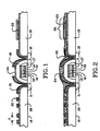
- Figs. 1-5 provide an example of a flowable dielectric according to the present invention
- Figs. 3 and 4 illustrate conceptually the equipment used to deposit the spin-on-glass layer
- Fig. 5 shows parameters of the resulting structure.
- Fig. 1 a cross sectional diagram of an integrated circuit structure is shown, where the line 10 represents the surface of an integrated circuit substrate, including for instance EPROM cells.
- An EPROM cell is formed therein having n-type buried diffusion regions 11 and 12 providing the source and drain for the memory cell.
- a thin insulator 13 is formed over the channel region of the EPROM device.
- a floating gate 14 is formed over the thin insulator 13.
- a dielectric 15 is formed over the floating gate, and a control gate, or word line, polysilicon layer 16 is formed over the dielectric 15.
- a side wall dielectric spacer 17 is formed on the side of the stack composed of the thin insulator 13, the floating gate 14, the dielectric 15 and the control gate, or word line, polysilicon layer 16.
- An insulating layer 18 is formed over the stack to isolate the control gate, or word line, polysilicon layer 16 from the metal layers following. This insulating layer also extends in the regions 19 and 20 to cover the semiconductor substrate.
- a metal contact 21 is formed in an opening established through the insulating layer 18 down to the buried diffusion region 11.
- metal lines 22 are patterned on the surface of the device for a variety of reasons. The device may have metal line spacings "X" on the order of six tenths of a micron. Also disposed on the integrated circuit over the region 19 is a metal contact pad 23.
- a high quality dielectric barrier 24 is formed over the underlying metal structures (21, 22, 23).
- the dielectric barrier 24 is formed of silicon oxynitride SION or silicon nitride using a plasma enhanced CVD process.
- the result of this process is a high quality barrier which blocks out moisture and mobile ions from reaching the underlying metal or other semiconductor structures.
- the opening over the metal contact 21 may be as narrow as 0.1 microns wide and 1.2 microns or more deep.
- Fig. 2 illustrates the result of the SOG process of the present invention, as a next step in defining a passivation layer.
- a flowable dielectric layer 25 is deposited. This dielectric layer is laid down using a spin coat of flowable glass to fill the gaps between the metal lines and to smooth out the wafer surface. The flowable glass is then cured at about 420 C° to solidify the glass.
- the properties of the spin-on-glass SOG after curing are targeted as follows:
- the flowable dielectric fills the gaps between the metal lines and the dimples within the contact holes and generally planarizes the underlying topography.
- the spin-on-glass layer is not etch backed. Further it is applied using a process which minimizes the thickness of the spin on dielectric in the region 26 generally over the metal contact pad 23.
- the spin-on-glass coating process consists of a dispense step, a spread step, and a dry setting step.
- a controlled amount of flow glass is dispensed under optimized dispense arm movement and wafer rotation speeds.
- a moveable cap making an enclosed compartment around the wafer, is then used to control the ambient above the wafer during the spin-spreading step.
- the pressure, temperature, and ambient gas composition can be controlled within the enclosed compartment.
- a saturated vapor ambient is kept inside the enclosed compartment to keep the glass under a highly flowable state during spreading.
- the centrifugal force due to the wafer rotation assists in the global smoothing of the flow glass.
- a high speed rotation is needed at the end of the spreading step to spin off the excess flow glass and reduce the flow glass thickness on top of large metal pads.
- the ambient is exhausted to dry and set the flow glass.
- the base line recipe for the SOG coating process is as follows: 1. Dispense SOG: Time (sec): 0-2 Spin Speed (rpm): 0-200 Acceleration (rpm/s): 500-2000 Exhaust (lpm): 0-200 Cup: open 2. Close Cap: Time (sec): 0-5 Spin Speed (rpm): 0 Acceleration (rpm/s):2000-3000 Exhaust (lpm): 0-200 Cup: closing 3.
- Spread/Flow-in Time (sec): 0-30 Spin Speed (rpm): 0-500 Acceleration (rpm/s): 1000-3000 Exhaust (lpm): 0-200 Cup: closed 4.
- the first step involves dispensing the SOG material such as commercially available siloxane polymer based materials, like Allied-Signal product numbers 512, 214 and 314.
- This step takes less than about 2 seconds with a final spin speed of less than about 200 revolutions per minute.
- the final spin speed is set rapidly with an acceleration rate of about 500-2000 rpm.
- Exhaust in the SOG chamber is set at less than about 200 liters per minute (lpm) with the cap open.
- the cap is closed. This process takes up to 5 seconds.
- the spin speed is set with a rapid deceleration from 2000-3000 rpm per second to 0 rpm.
- the exhaust during the cap closing step is set at up to about 200 lpm.
- the SOG material is spread and flowed in. This process takes up to about 30 seconds, preferably greater than about 20 seconds, with a relatively low spin speed of up to about 500 rpm, preferably less than about 250 rpm.
- the spin speed is set with an acceleration rate of about 1000 - 3000 rpm per second with the exhaust in the outside chamber at a value up to about 200 lpm.
- the cap is closed, isolating the space inside the closed cap from the external exhaust, so that the evaporation rate of the SOG solvent is slowed down.
- the cap is opened.
- This step takes about up to 5 seconds with a 0 rpm spin speed.
- the spinning is stopped with a deceleration in a range of 2000-3000 rpm per second.
- the exhaust is set at a value of up to about 400 lpm while the cap is being opened.
- the final step is the spin off step which takes up to about 20 seconds.
- the wafer rotates at a value between 3000-5000 rpm.
- the final spin speed is reached with rapid acceleration in the range of 5000-10000 rpm/s.
- the exhaust in the chamber is up to about 400 lpm with the cap open.
- This process allows much longer spread/ flow-in time and a much lower spread/flow-in rotation speed compared to prior art systems, and achieves superior planarity, and accomplishes a thin SOG layer over the metal contact pads without an etch back step.
- the spin-on-glass equipment includes a spin-on-glass coating chamber, generally 50, which includes a support 51 for an integrated circuit 52.
- the support 51 is mounted on a shaft 53 which is coupled to a motor 54 for spinning the support 51.
- the chamber 50 is coupled through outlet 55 to an exhaust system.
- Inlet 56 may be used for such purposes as known in the art.
- a motor 57 coupled to an extendable shaft 58 which supports a cover structure 59.
- the motor 57 and motor 54 are operated synchronously, such that the cover 59 and the support 51 may be spinned at the same rate.
- the periphery, generally 60, of the cover may comprise an elastic projection which is laid on the upward facing region of the support 51 or the integrated circuit wafer 52, as suits the needs of the particular application.
- a mechanism 61 is provided for dispensing solvent containing spin-on-glass material 62 on the integrated circuit 52.
- Fig. 4 illustrates the chamber of Fig. 3 with the cover 59 lowered over the integrated circuit 52.
- the shaft 58 connecting the cover 59 to the motor 57 is extended so that the cover encloses the integrated circuit and establishes a controllable environment, generally 63, over the integrated circuit 52.
- Fig. 4 also illustrates schematically that a source of ambient control gases, generally 70, may be coupled to the shaft 53 and supplied into the controllable environment 63 through the shaft 53 using techniques known in the art.
- the temperature of the integrated circuit 52 may be controlled by a temperature control system, generally 71, which controls the temperature of the support member 51 during the spinning processes.
- the controllable environment 63 may be passively controlled by simply enclosing the integrated circuit during the spread and flow in spinning process. This will control the evaporation rate of the solvent used to carry the spin-on-glass during these steps.
- an active control system may be applied, in which the ambient control gases 70 are injected into the region 63 to control the vapor pressure of selected materials in the environment 63.
- the temperature of the integrated circuit 52 may be controlled during these processes using temperature control systems 71.
- a combination of environmental controls might be applied to engineer the spin-on-glass material characteristics according to the need of the particular design.
- Fig. 5 shows a structure including the spin-on-glass material of the present invention illustrate certain characteristics of the process.
- the integrated circuit substrate surface is shown at line 100.
- a metal structure 101 is deposited.
- a CVD dielectric 102 is deposited over the metal structure 101.
- a spin-on-glass material 103 is deposited over the CVD dielectric 102.
- Fig. 5 The dimensions of the structure in Fig. 5 include the following:
- DOP (1-dh/a) x 100%
- the DOP depends on the aspect ratio defined as a/L of the underlying gap or trench feature, and on the strength of the centrifugal and surface tension forces occurring during the SOG process.
- the DOP can be plotted as a function of the aspect ratio and a parameter B as in Fig. 6, where the parameter B is defined as the centrifugal force divided by the surface tension. In principle at small B, the lower the spin speed (a smaller centrifugal force) and higher surface tension of SOG will improve the DOP.
- the viscosity term is assumed constant and negligible in nonvolatile fluid model such as illustrated in the Yonkoski, et al. reference.
- both viscosity and surface tension are continuously changing properties due to the evaporation of the solvent in the SOG during the spin coating process of the prior art.
- the SOG will solidify so fast that it will not flow to the edge of the wafers.
- the top layer of the SOG can be modified by introducing saturated vapor solvents into the closed cap ambient, or dispensing liquid solvent directly on the wafer surface before closing the cap for the step 7 flow in. This will create a graded solvent content profile across the thickness of the SOG such that the surface of the SOG has a higher solvent content than the deeper layers. This will allow a very high spin off speed, while preventing the SOG in deep features of the substrate from being dislodged. A fine shaping of the surface profile of the SOG may therefore be achieved.
- the coating technique of the present invention results in better planarity and gap filling than prior art systems.
- the coating technique can be applied to areas other than flowable dielectrics in integrated circuits.
- the principle applies to any process that involves coating a volatile flowable material, and wherein the process results can be improved by controlling the ambient conditions.
Landscapes
- Formation Of Insulating Films (AREA)
- Application Of Or Painting With Fluid Materials (AREA)
- Coating Apparatus (AREA)
- Encapsulation Of And Coatings For Semiconductor Or Solid State Devices (AREA)
Description
- The present invention relates to planarization processes used during integrated circuit manufacturing; and more particularly to an improved spin-on-glass process in which the environment is controlled during the spread/flow-in step and other steps of the process.
- Spin-on-glass (SOG) has been widely used in integrated circuit manufacturing to improve wafer surface planarity. A high degree of planarity on the wafer surface is needed for fine photolithographic resolution. Also, planarity is needed to avoid metal stringers after etching of the metal lines which might be left in impressions on the surface of the wafer and cause shorts on the device. Many articles have been published, for instance, in the annual VLSI Multilevel Interconnection Conferences, such as Ting, et al., "Planarization Process Using Spin-On-Glass", Proceedings Fourth International IEEE VLSI Multilevel Interconnection Conference, June 15-16, 1987, pages 61-67. Also, background concerning the SOG coating principles can be found in Yonkoski, et al., "A Mathematical Model for Planarization of Microelectronic Topographies", Journal of the Electrochemical Society, Vol 141, No. 2, February 1994, pages 585-593; and Sukanek, "A Model for Spin Coating with Topography", Journal of the Electrochemical Society, Vol. 136, No. 10, October 1989, pages 3019-3026.
- Many factors affect the results of a SOG coating profile. Properties of the materials used, including the surface tension, viscosity, solvent evaporation rate, and shrinkage due to high temperature curing are key factors in the ability of the SOG process to fill gaps and establish a planar surface. However, spin speed, SOG settling time, acceleration, the manner of dispensing the SOG, and the ambient during the coating process are important factors for establishing a quality coat on the device. There are many interacting factors involved in the SOG coating process including surface tension, SOG bulk viscosity, centrifugal force, and gravitational forces that the SOG experiences.
- A conventional SOG coating process typically consists of the following steps:
- 1) Dispense SOG at a low wafer spin speed (e.g. 0-200 RPM).
- 2) Spread SOG at a medium spin speed to get uniform wafer coverage (e.g. 500-1000 RPM).
- 3) Flow-in (planarize) SOG at a slow speed (e.g. 500-1000 RPM).
- 4) Spin off the excess top layer SOG at a high speed (e.g. 2000-3000 RPM).
- 5) Transfer the wafer from the coater to a hot plate.
- 6) Bake/dry the SOG at higher temperatures.
-
- There are several limitations to the conventional SOG coating process. First, there is a lower limit as to how slow the wafer may be spinned during the spread step, and a maximum amount of time during which the flow in step may be allowed to occur to avoid rapid viscosity changes due to loss of solvent. Further, the spin off rotation speed during the fourth step needs to be high enough to minimize excess SOG thickness on the top of wide metal structures. However, the spin off rotation speed cannot be too high such that unhardened SOG escapes filled in gaps in the underlying structure, leaving a void behind.
- Further background concerning SOG coating process can be seen in U.S. Patent No. 4,721,548 by Morimoto (SOG with etch back for semiconductor planarization); U.S. Patent No. 4,775,550 by Chu, et al. (SOG with etch back for intermetal dielectric); U.S. Patent No. 4,885,262 by Ting, et al. (chemically modified SOG); U.S. Patent No. 5,003,062 by Yen (planarization process); U.S. Patent No. 5,106,787 by Yen (high vacuum curing for SOG planarization).
- US 5,013,586 relates to a technique for the uniformly even application of a resin coating on a substrate. The substrate is placed on a rotary plate so that rotation provokes spreading of a thin coating of the resin over the substrate. A cover is provided over the plate to confine a gaseous suspended solvent.
- US 4,714,926 relates to spin-coating of a substrate with a resin material in a dual spin cycle. The substrate is spun, coated and continued to spin until the resin is dry.
- Accordingly, it is desirable to provide a spin-on-glass process resulting in better filling of voids, better planarity, and thinner structures over wide metal features on the device.
- According to one aspect of the present invention there is provided a process for applying flowable dielectric during manufacture of an integrated circuit, comprising the steps of: A) supporting the integrated circuit in a chamber; B) dispensing the flowable dielectric in a solvent on the integrated circuit in the chamber; C) covering the integrated circuit to provide a controllable environment within the chamber after the step of dispensing; D) spinning the integrated circuit while controlling the controllable environment to spread and flow-in the flowable dielectric; E) uncovering the integrated circuit within the chamber; F) spinning the integrated circuit to spin off excess flowable dielectric; and G) curing the flowable dielectric.
- Embodiments of the present invention provide an improved process for spreading and flowing in a flowable material on an irregular substrate, such as a flowable dielectric on integrated circuit during manufacture, which results in greater planarity and better gap filling ability. The process involves spinning the irregular substrate while controlling evaporation of the solvent from the flowable material to increase the amount of flow-in time and decrease spin velocity during flow in to improve planarity and gap filling ability.
- Thus, embodiments of the invention can be characterized as a process for applying a flowable dielectric, such as spin-on-glass, during manufacturing of an integrated circuit. The process comprises
supporting the integrated circuit in a chamber;
dispensing a solvent containing flowable dielectric on the integrated circuit in the chamber;
covering the integrated circuit to provide a controllable environment around the integrated circuit after the step of dispensing;
spinning the integrated circuit while controlling the controllable environment to spread and flow in the flowable dielectric;
uncovering the integrated circuit within the chamber;
spinning the integrated circuit to spin off flowable dielectric; and
curing the flowable dielectric. - The environment surrounding the integrated circuit is controlled to slow down evaporation of the solvent, either passively by merely enclosing the integrated circuit during the spread and flow in process within a limited space, or actively, such as by controlling the vapor pressure of selected materials, controlling the temperature of the integrated circuit, or controlling other parameters of the environment.
- The process according to embodiments of the present invention allows the step of spinning the integrated circuit for the purpose of spreading and flowing in to be accomplished at a lower speed, such as at less than 500 RPM. Also, the process provides for allowing a longer spread and flow in time, such as greater than two seconds and up to thirty seconds or more. Furthermore, because of the better spreading and flowing in process, a higher speed for spinning off the spin-on-glass can be utilized, such as greater than 3000 RPM, resulting in a thinner dielectric over the wide metal areas on the device.
- Because of the ability to control the wafer ambient with the moveable cap according to embodiments of the present invention, even further engineering of the SOG process can be achieved. For instance, after the spread and flow in step, the cap may be opened and the integrated circuit exposed to the ambient, to allow the solvent to evaporate so that most of the solvent is removed. During exposure to the ambient, the integrated circuit may also be exposed to a bake or drying process to aid in removing the solvent from the deposited layer. After this step, the top layer of the SOG can be modified, such that a thin layer of it is made flowable. Then, a flow in process is executed again. These steps can be iterated to achieve ultimate planarity on the device. Finally, the excess top layer is spun off at high speed and the SOG is cured by baking and drying as before.
- The top layer of the SOG can be modified according to the process described above by either introducing saturated vapor solvents into the ambient with the cap closed, or dispensing a liquid solvent directly onto the wafer surface. The solvent content of the modified top layer will be higher than the solvent content of deeper layers of the SOG. This will allow a very high spin off speed, such that the lower solvent content deeper layers will not be dislodged, while the top layers achieve very high planarity.
- Thus, a new coating scheme in which one controls the wafer ambient environment, during the spread and flow in step, or any other step in which SOG characteristics can be controlled, is provided. By controlling the intrinsic environmental parameters, the surface profile of the spin-on-glass can be engineered as needed.
- Other aspects and advantages of the present invention can be seen upon review of the figures, the detailed description in the claims which follow.
-
- Fig. 1 is a schematic diagram of an integrated circuit structure on which a flowable dielectric may be applied.
- Fig. 2 is an illustration of the structure of Fig. 1 having the flowable dielectric thereon.
- Fig. 3 is a conceptual diagram of the spin-on-glass coating chamber including a cover according the present invention.
- Fig. 4 illustrates the coating chamber of Fig. 3 having the cover closed over the integrated circuit and providing a controllable environment.
- Fig. 5 is a schematic diagram of the flowable dielectric according to the present invention used to illustrate certain features of the invention.
- Fig. 6 is a graph illustrating parameters associated with the spin-on-glass process, taken from Yonkoski, et al., cited above.
-
- The detailed description of the present invention is provided with respect to Figs. 1-5, in which Figs. 1 and 2 provide an example of a flowable dielectric according to the present invention, Figs. 3 and 4 illustrate conceptually the equipment used to deposit the spin-on-glass layer, and Fig. 5 shows parameters of the resulting structure.
- In Fig. 1, a cross sectional diagram of an integrated circuit structure is shown, where the
line 10 represents the surface of an integrated circuit substrate, including for instance EPROM cells. An EPROM cell is formed therein having n-type burieddiffusion regions thin insulator 13 is formed over the channel region of the EPROM device. A floatinggate 14 is formed over thethin insulator 13. A dielectric 15 is formed over the floating gate, and a control gate, or word line,polysilicon layer 16 is formed over the dielectric 15. A side walldielectric spacer 17 is formed on the side of the stack composed of thethin insulator 13, the floatinggate 14, the dielectric 15 and the control gate, or word line,polysilicon layer 16. An insulatinglayer 18 is formed over the stack to isolate the control gate, or word line,polysilicon layer 16 from the metal layers following. This insulating layer also extends in theregions metal contact 21 is formed in an opening established through the insulatinglayer 18 down to the burieddiffusion region 11. Also,metal lines 22 are patterned on the surface of the device for a variety of reasons. The device may have metal line spacings "X" on the order of six tenths of a micron. Also disposed on the integrated circuit over theregion 19 is ametal contact pad 23. - A high
quality dielectric barrier 24 is formed over the underlying metal structures (21, 22, 23). Thedielectric barrier 24 is formed of silicon oxynitride SION or silicon nitride using a plasma enhanced CVD process. - The result of this process is a high quality barrier which blocks out moisture and mobile ions from reaching the underlying metal or other semiconductor structures.
- After the growth of the high
quality dielectric barrier 24, the opening over themetal contact 21 may be as narrow as 0.1 microns wide and 1.2 microns or more deep. - Fig. 2 illustrates the result of the SOG process of the present invention, as a next step in defining a passivation layer. According to the next step, a
flowable dielectric layer 25 is deposited. This dielectric layer is laid down using a spin coat of flowable glass to fill the gaps between the metal lines and to smooth out the wafer surface. The flowable glass is then cured at about 420 C° to solidify the glass. The properties of the spin-on-glass SOG after curing are targeted as follows: - thickness (Angstroms): 2000 to 5500
- refractive index: 1.3-1.4
- gap fill: complete fill of 0.1µm wide and > 1.2 µm deep gaps.
- planarity: >90% at large metal spacings (> 40µm metal spacing)
- SOG thickness on top of large metal pad (Angstroms): <1000
- stress: 2x10⁻¹ - 7x10⁻¹ Nm2 (2 E8 - 7 E8 dynes/cm2) tensile.
-
- Thus, the flowable dielectric fills the gaps between the metal lines and the dimples within the contact holes and generally planarizes the underlying topography.
- The spin-on-glass layer is not etch backed. Further it is applied using a process which minimizes the thickness of the spin on dielectric in the
region 26 generally over themetal contact pad 23. - The spin-on-glass coating process consists of a dispense step, a spread step, and a dry setting step. In the dispense step, a controlled amount of flow glass is dispensed under optimized dispense arm movement and wafer rotation speeds. A moveable cap, making an enclosed compartment around the wafer, is then used to control the ambient above the wafer during the spin-spreading step. During the spreading step, the pressure, temperature, and ambient gas composition can be controlled within the enclosed compartment. Typically, a saturated vapor ambient is kept inside the enclosed compartment to keep the glass under a highly flowable state during spreading. The centrifugal force due to the wafer rotation assists in the global smoothing of the flow glass. A high speed rotation is needed at the end of the spreading step to spin off the excess flow glass and reduce the flow glass thickness on top of large metal pads. At the last dry setting step, the ambient is exhausted to dry and set the flow glass.
- The base line recipe for the SOG coating process is as follows:
1. Dispense SOG: Time (sec): 0-2 Spin Speed (rpm): 0-200 Acceleration (rpm/s): 500-2000 Exhaust (lpm): 0-200 Cup: open 2. Close Cap: Time (sec): 0-5 Spin Speed (rpm): 0 Acceleration (rpm/s):2000-3000 Exhaust (lpm): 0-200 Cup: closing 3. Spread/Flow-in: Time (sec): 0-30 Spin Speed (rpm): 0-500 Acceleration (rpm/s): 1000-3000 Exhaust (lpm): 0-200 Cup: closed 4. Open Cap: Time (sec): 0-5 Spin Speed (rpm): 0 Acceleration (rpm/s): 2000-3000 Exhaust (lpm): 0-400 Cup: opening 5. Spinoff: Time (sec): 0-20 Spin Speed (rpm): 3000-5000 Acceleration (rpm/s): 5000-10000 Exhaust (lpm): 0-400 Cup: open - Thus, the first step involves dispensing the SOG material such as commercially available siloxane polymer based materials, like Allied-Signal product numbers 512, 214 and 314. This step takes less than about 2 seconds with a final spin speed of less than about 200 revolutions per minute. The final spin speed is set rapidly with an acceleration rate of about 500-2000 rpm. Exhaust in the SOG chamber is set at less than about 200 liters per minute (lpm) with the cap open.
- After the dispense step, the cap is closed. This process takes up to 5 seconds. The spin speed is set with a rapid deceleration from 2000-3000 rpm per second to 0 rpm. The exhaust during the cap closing step is set at up to about 200 lpm.
- After the cap is closed, the SOG material is spread and flowed in. This process takes up to about 30 seconds, preferably greater than about 20 seconds, with a relatively low spin speed of up to about 500 rpm, preferably less than about 250 rpm. The spin speed is set with an acceleration rate of about 1000 - 3000 rpm per second with the exhaust in the outside chamber at a value up to about 200 lpm. During this process, the cap is closed, isolating the space inside the closed cap from the external exhaust, so that the evaporation rate of the SOG solvent is slowed down.
- In the next step, the cap is opened. This step takes about up to 5 seconds with a 0 rpm spin speed. The spinning is stopped with a deceleration in a range of 2000-3000 rpm per second. The exhaust is set at a value of up to about 400 lpm while the cap is being opened.
- The final step is the spin off step which takes up to about 20 seconds. During spin off, the wafer rotates at a value between 3000-5000 rpm. The final spin speed is reached with rapid acceleration in the range of 5000-10000 rpm/s. The exhaust in the chamber is up to about 400 lpm with the cap open.
- This process allows much longer spread/ flow-in time and a much lower spread/flow-in rotation speed compared to prior art systems, and achieves superior planarity, and accomplishes a thin SOG layer over the metal contact pads without an etch back step.
- The equipment utilized to form the foregoing process steps is conceptually illustrated in Figs. 3 and 4. Mechanically, this equipment can be implemented described for instance in German Patent Application No. DE 4203913, filed February 11, 1992, invented by Gabriel, et al., except modified for the smaller dimensions of a semiconductor wafer.
- As shown in Fig. 3, the spin-on-glass equipment includes a spin-on-glass coating chamber, generally 50, which includes a
support 51 for anintegrated circuit 52. Thesupport 51 is mounted on ashaft 53 which is coupled to amotor 54 for spinning thesupport 51. Thechamber 50 is coupled throughoutlet 55 to an exhaust system.Inlet 56 may be used for such purposes as known in the art. - Also coupled to the
chamber 50 is amotor 57 coupled to anextendable shaft 58 which supports acover structure 59. Themotor 57 andmotor 54 are operated synchronously, such that thecover 59 and thesupport 51 may be spinned at the same rate. The periphery, generally 60, of the cover may comprise an elastic projection which is laid on the upward facing region of thesupport 51 or theintegrated circuit wafer 52, as suits the needs of the particular application. Also, amechanism 61 is provided for dispensing solvent containing spin-on-glass material 62 on theintegrated circuit 52. - Fig. 4 illustrates the chamber of Fig. 3 with the
cover 59 lowered over theintegrated circuit 52. Theshaft 58 connecting thecover 59 to themotor 57 is extended so that the cover encloses the integrated circuit and establishes a controllable environment, generally 63, over theintegrated circuit 52. - Fig. 4 also illustrates schematically that a source of ambient control gases, generally 70, may be coupled to the
shaft 53 and supplied into thecontrollable environment 63 through theshaft 53 using techniques known in the art. Similarly, the temperature of theintegrated circuit 52 may be controlled by a temperature control system, generally 71, which controls the temperature of thesupport member 51 during the spinning processes. Thus, thecontrollable environment 63 may be passively controlled by simply enclosing the integrated circuit during the spread and flow in spinning process. This will control the evaporation rate of the solvent used to carry the spin-on-glass during these steps. Alternatively, an active control system may be applied, in which theambient control gases 70 are injected into theregion 63 to control the vapor pressure of selected materials in theenvironment 63. Also, the temperature of theintegrated circuit 52 may be controlled during these processes usingtemperature control systems 71. A combination of environmental controls might be applied to engineer the spin-on-glass material characteristics according to the need of the particular design. - Fig. 5 shows a structure including the spin-on-glass material of the present invention illustrate certain characteristics of the process. In Fig. 5, the integrated circuit substrate surface is shown at
line 100. On the surface, ametal structure 101 is deposited. ACVD dielectric 102 is deposited over themetal structure 101. A spin-on-glass material 103 is deposited over theCVD dielectric 102. - The dimensions of the structure in Fig. 5 include the following:
- h:
- SOG thickness in a wide open trench.
- a:
- initial step height of the integrated circuit structure before SOG coating.
- dh:
- a maximum height difference of the SOG coating on the integrated circuit.
- L:
- the width of the trench prior to deposition of the SOG.
- t:
- maximum thickness of the SOG on top of metal.
- Adopting the definition of the degree of planarity (DOP) as described in the Yonkoski, et al. reference cited above, the degree of planarity is defined by the following equation:
- Further engineering of the SOG can be provided using the moveable cap which allows for selective control of the environment over the integrated circuit during selected spinning steps of the process.
Thus, a process might be executed as follows: - 1) dispense SOG,
- 2) enclose the wafer in a controlled environment where the SOG solvent loss will be minimized,
- 3) spread the SOG,
- 4) flow in the SOG,
- 5) exhaust the ambient, bake/dry the SOG so that the solvent is almost gone,
- 6) modify the top layer of the SOG, such that a thin layer of SOG is made flowable,
- 7) flow in the SOG as modified,
- 8) steps 5-7 may be iterated to achieve ultimate planarity,
- 9) spin off the excess top layer of SOG at high speed,
- 10) bake/dry the SOG for final curing.
-
- The top layer of the SOG can be modified by introducing saturated vapor solvents into the closed cap ambient, or dispensing liquid solvent directly on the wafer surface before closing the cap for the step 7 flow in. This will create a graded solvent content profile across the thickness of the SOG such that the surface of the SOG has a higher solvent content than the deeper layers. This will allow a very high spin off speed, while preventing the SOG in deep features of the substrate from being dislodged. A fine shaping of the surface profile of the SOG may therefore be achieved.
- The coating technique of the present invention results in better planarity and gap filling than prior art systems. The coating technique can be applied to areas other than flowable dielectrics in integrated circuits. In particular, the principle applies to any process that involves coating a volatile flowable material, and wherein the process results can be improved by controlling the ambient conditions.
- The foregoing description of a preferred embodiment of the invention has been presented for purposes of illustration and description. It is not intended to be exhaustive or to limit the invention to the precise forms disclosed. Obviously, many modifications and variations will be apparent to practitioners skilled in this art. It is intended that the scope of the invention be defined by the following claims and their equivalents.
Claims (20)
- A process for applying flowable dielectric layer (25) during manufacture of an integrated circuit (52), comprising the steps of:A) supporting the integrated circuit in a chamber (50);B) dispensing the flowable dielectric in a solvent on the integrated circuit in the chamber;C) covering the integrated circuit to provide a controllable environment within the chamber after the step of dispensing;D) spinning the integrated circuit while controlling the controllable environment to spread and flow-in the flowable dielectric;E) uncovering the integrated circuit within the chamber;F) spinning the integrated circuit to spin off excess flowable dielectric; andG) curing the flowable dielectric.
- The process of claim 1, including after said step D the steps of:causing evaporation of solvent from the flowable dielectric to reduce the amount of solvent in the flowable dielectric,modifying the surface of the flowable dielectric, so that at least a top surface layer is made flowable, andspinning the integrated circuit again, to flow-in the modified top layer of the flowable dielectric.
- The process of claim 1 or 2, wherein the step of spinning the integrated circuit while controlling the controllable environment includes slowing down evaporation of the solvent.
- The process of claim 1 or 2, wherein the step of spinning the integrated circuit while controlling the controllable environment includes passively slowing down evaporation of the solvent.
- The process of claim 1 or 2, wherein the step of spinning the integrated circuit while controlling the controllable environment includes actively controlling vapor pressure in the controllable environment for selected materials.
- The process of claim 1 or 2, wherein the step of spinning the integrated circuit while controlling the controllable environment includes controlling temperature of the integrated circuit.
- The process of claim 1 or 2, wherein the step of spinning the integrated circuit while controlling the controllable environment includes spinning the integrated circuit at less than 500 revolutions per minute.
- The process of claim 1 or 2, wherein the step of spinning the integrated circuit while controlling the controllable environment includes spinning the integrated circuit at less than 250 revolutions per minute.
- The process of claim 1 or 2, wherein the step of spinning the integrated circuit while controlling the controllable environment includes spinning the integrated circuit for longer than 2 seconds.
- The process of claim 1 or 2, wherein the step of spinning the integrated circuit while controlling the controllable environment includes spinning the integrated circuit for longer than 20 seconds.
- The process of claim 1 or 2, wherein the step of spinning the integrated circuit while controlling the controllable environment includes spinning the integrated circuit at less than 500 revolutions per minute for longer than 2 seconds.
- The process of claim 1 or 2, wherein the step of spinning the integrated circuit to spin off excess flowable dielectric comprises spinning the integrated circuit at more than 3000 revolutions per minute.
- The process of claim 1, where the flowable dielectric layer (25) is spin-on-glass and step (D) comprises,
spinning the integrated circuit at less than 500 revolutions per minute for longer than 2 seconds while controlling the controllable environment to spread and flow-in the spin-on-glass. - The process of claim 13, wherein the spin-on-glass comprises a siloxane polymer.
- The process of claim 13, wherein the step of spinning the integrated circuit while controlling the controllable environment includes slowing down evaporation of the solvent.
- The process of claim 13, wherein the step of spinning the integrated circuit while controlling the controllable environment includes passively slowing down evaporation of the solvent.
- The process of claim 13, wherein the step of spinning the integrated circuit while controlling the controllable environment includes actively controlling vapor pressure in the controllable environment for selected materials.
- The process of claim 13, wherein the step of spinning the integrated circuit while controlling the controllable environment includes controlling temperature of the integrated circuit.
- The process of claim 13, wherein the step of spinning the integrated circuit to spin off excess flowable dielectric comprises spinning the integrated circuit at more than 3000 revolutions per minute.
- The process of claim 1, wherein the flowable dielectric layer (25) is spin-on-glass and step (C) comprises:covering the integrated circuit to provide a controllable environment within the chamber after the step of dispensing, so the evaporation of the solvent is controlled, the method including after step (D) the steps of:causing evaporation of a portion of the solvent and establishing a flowable top layer in the deposited spin-on-glass with less flowable lower layers; andspinning the integrated circuit again to flow in the flowable top layer of the spin-on-glass.
Applications Claiming Priority (1)
| Application Number | Priority Date | Filing Date | Title |
|---|---|---|---|
| PCT/US1994/012785 WO1996014164A1 (en) | 1994-11-07 | 1994-11-07 | Spin-on-glass process with controlled environment |
Publications (3)
| Publication Number | Publication Date |
|---|---|
| EP0738185A1 EP0738185A1 (en) | 1996-10-23 |
| EP0738185A4 EP0738185A4 (en) | 2000-04-19 |
| EP0738185B1 true EP0738185B1 (en) | 2003-07-30 |
Family
ID=22243241
Family Applications (1)
| Application Number | Title | Priority Date | Filing Date |
|---|---|---|---|
| EP95901797A Expired - Lifetime EP0738185B1 (en) | 1994-11-07 | 1994-11-07 | Spin-on-glass process with controlled environment |
Country Status (4)
| Country | Link |
|---|---|
| EP (1) | EP0738185B1 (en) |
| JP (1) | JPH09511449A (en) |
| DE (1) | DE69432989T2 (en) |
| WO (1) | WO1996014164A1 (en) |
Families Citing this family (3)
| Publication number | Priority date | Publication date | Assignee | Title |
|---|---|---|---|---|
| US6254931B1 (en) * | 1996-10-28 | 2001-07-03 | Robert D. Herpst | Method and apparatus for the production of thin films |
| US6335296B1 (en) | 1998-08-06 | 2002-01-01 | Alliedsignal Inc. | Deposition of nanoporous silica films using a closed cup coater |
| JP6437405B2 (en) * | 2015-09-10 | 2018-12-12 | 東芝メモリ株式会社 | Spin coating method and electronic component manufacturing method |
Family Cites Families (6)
| Publication number | Priority date | Publication date | Assignee | Title |
|---|---|---|---|---|
| US4741926A (en) * | 1985-10-29 | 1988-05-03 | Rca Corporation | Spin-coating procedure |
| JP2649156B2 (en) * | 1987-02-13 | 1997-09-03 | 東京エレクトロン 株式会社 | Resist coating apparatus and method |
| JPH0451907Y2 (en) * | 1987-09-18 | 1992-12-07 | ||
| FR2636546B1 (en) * | 1988-09-15 | 1991-03-15 | Sulzer Electro Tech | METHOD AND DEVICE FOR THE UNIFORMLY REGULAR APPLICATION OF A RESIN LAYER ON A SUBSTRATE |
| US4885262A (en) * | 1989-03-08 | 1989-12-05 | Intel Corporation | Chemical modification of spin-on glass for improved performance in IC fabrication |
| DE4203913C2 (en) * | 1992-02-11 | 1996-09-19 | Fairchild Convac Gmbh Geraete | Method and device for applying and / or for partially removing a thin layer on or from a substrate |
-
1994
- 1994-11-07 DE DE69432989T patent/DE69432989T2/en not_active Expired - Lifetime
- 1994-11-07 WO PCT/US1994/012785 patent/WO1996014164A1/en not_active Ceased
- 1994-11-07 JP JP8515260A patent/JPH09511449A/en active Pending
- 1994-11-07 EP EP95901797A patent/EP0738185B1/en not_active Expired - Lifetime
Also Published As
| Publication number | Publication date |
|---|---|
| EP0738185A1 (en) | 1996-10-23 |
| DE69432989D1 (en) | 2003-09-04 |
| DE69432989T2 (en) | 2004-05-27 |
| JPH09511449A (en) | 1997-11-18 |
| WO1996014164A1 (en) | 1996-05-17 |
| EP0738185A4 (en) | 2000-04-19 |
Similar Documents
| Publication | Publication Date | Title |
|---|---|---|
| US6004622A (en) | Spin-on-glass process with controlled environment | |
| EP0738424B1 (en) | Integrated circuit passivation process | |
| US6407009B1 (en) | Methods of manufacture of uniform spin-on films | |
| US5716673A (en) | Spin-on-glass process with controlled environment | |
| US4676867A (en) | Planarization process for double metal MOS using spin-on glass as a sacrificial layer | |
| US6530340B2 (en) | Apparatus for manufacturing planar spin-on films | |
| US6317642B1 (en) | Apparatus and methods for uniform scan dispensing of spin-on materials | |
| US6387825B2 (en) | Solution flow-in for uniform deposition of spin-on films | |
| KR100266428B1 (en) | Semiconductor device and method for manufacturing | |
| US5453406A (en) | Aspect ratio independent coating for semiconductor planarization using SOG | |
| US6946407B2 (en) | Method for pretreating a substrate prior to application of a polymeric coat | |
| EP0738185A1 (en) | Spin-on-glass process with controlled environment | |
| US6020265A (en) | Method for forming a planar intermetal dielectric layer | |
| US6136729A (en) | Method for improving semiconductor dielectrics | |
| US20240387188A1 (en) | Ambient controlled two-step thermal treatment for spin-on coating layer planarization | |
| US20070087582A1 (en) | Gas jet reduction of iso-dense field thickness bias for gapfill process | |
| Hirasawa et al. | Analysis of drying shrinkage and flow due to surface tension of spin-coated films on topographic substrates | |
| US6613700B2 (en) | Method for spin coating high viscosity materials on silicon wafers | |
| US5913979A (en) | Method for removing spin-on-glass at wafer edge | |
| US5918152A (en) | Gap filling method using high pressure | |
| US6485576B1 (en) | Method for removing coating bead at wafer flat edge | |
| US20070128887A1 (en) | Spin-on glass passivation process | |
| US20040248426A1 (en) | Edge peeling improvement of low-k dielectric materials stack by adjusting EBR resistance | |
| US12629725B2 (en) | Method and single wafer processing system for processing of semiconductor wafers | |
| US20250044699A1 (en) | Film deposition method, method for manufacturing device, and film deposition apparatus |
Legal Events
| Date | Code | Title | Description |
|---|---|---|---|
| PUAI | Public reference made under article 153(3) epc to a published international application that has entered the european phase |
Free format text: ORIGINAL CODE: 0009012 |
|
| 17P | Request for examination filed |
Effective date: 19960712 |
|
| AK | Designated contracting states |
Kind code of ref document: A1 Designated state(s): DE FR GB IT NL |
|
| RAP1 | Party data changed (applicant data changed or rights of an application transferred) |
Owner name: MACRONIX INTERNATIONAL CO., LTD. |
|
| A4 | Supplementary search report drawn up and despatched |
Effective date: 20000308 |
|
| AK | Designated contracting states |
Kind code of ref document: A4 Designated state(s): DE FR GB IT NL |
|
| RAP1 | Party data changed (applicant data changed or rights of an application transferred) |
Owner name: MACRONIX INTERNATIONAL CO., LTD. |
|
| 17Q | First examination report despatched |
Effective date: 20010830 |
|
| GRAH | Despatch of communication of intention to grant a patent |
Free format text: ORIGINAL CODE: EPIDOS IGRA |
|
| GRAH | Despatch of communication of intention to grant a patent |
Free format text: ORIGINAL CODE: EPIDOS IGRA |
|
| GRAA | (expected) grant |
Free format text: ORIGINAL CODE: 0009210 |
|
| AK | Designated contracting states |
Designated state(s): DE FR GB IT NL |
|
| REG | Reference to a national code |
Ref country code: GB Ref legal event code: FG4D |
|
| REF | Corresponds to: |
Ref document number: 69432989 Country of ref document: DE Date of ref document: 20030904 Kind code of ref document: P |
|
| ET | Fr: translation filed | ||
| PLBE | No opposition filed within time limit |
Free format text: ORIGINAL CODE: 0009261 |
|
| STAA | Information on the status of an ep patent application or granted ep patent |
Free format text: STATUS: NO OPPOSITION FILED WITHIN TIME LIMIT |
|
| 26N | No opposition filed |
Effective date: 20040504 |
|
| PGFP | Annual fee paid to national office [announced via postgrant information from national office to epo] |
Ref country code: GB Payment date: 20131106 Year of fee payment: 20 Ref country code: FR Payment date: 20131108 Year of fee payment: 20 Ref country code: DE Payment date: 20131030 Year of fee payment: 20 |
|
| PGFP | Annual fee paid to national office [announced via postgrant information from national office to epo] |
Ref country code: NL Payment date: 20131109 Year of fee payment: 20 Ref country code: IT Payment date: 20131107 Year of fee payment: 20 |
|
| REG | Reference to a national code |
Ref country code: DE Ref legal event code: R071 Ref document number: 69432989 Country of ref document: DE |
|
| REG | Reference to a national code |
Ref country code: NL Ref legal event code: V4 Effective date: 20141107 |
|
| REG | Reference to a national code |
Ref country code: GB Ref legal event code: PE20 Expiry date: 20141106 |
|
| PG25 | Lapsed in a contracting state [announced via postgrant information from national office to epo] |
Ref country code: GB Free format text: LAPSE BECAUSE OF EXPIRATION OF PROTECTION Effective date: 20141106 |