EP0732725B1 - Method for identifying surface atoms of solid sample and apparatus therefor - Google Patents
Method for identifying surface atoms of solid sample and apparatus therefor Download PDFInfo
- Publication number
- EP0732725B1 EP0732725B1 EP96301728A EP96301728A EP0732725B1 EP 0732725 B1 EP0732725 B1 EP 0732725B1 EP 96301728 A EP96301728 A EP 96301728A EP 96301728 A EP96301728 A EP 96301728A EP 0732725 B1 EP0732725 B1 EP 0732725B1
- Authority
- EP
- European Patent Office
- Prior art keywords
- sample
- deposits
- rays
- island
- fluorescent
- Prior art date
- Legal status (The legal status is an assumption and is not a legal conclusion. Google has not performed a legal analysis and makes no representation as to the accuracy of the status listed.)
- Expired - Lifetime
Links
- 238000000034 method Methods 0.000 title claims description 18
- 239000007787 solid Substances 0.000 title claims description 6
- 238000010894 electron beam technology Methods 0.000 claims description 20
- 239000000126 substance Substances 0.000 claims description 11
- 239000010949 copper Substances 0.000 claims description 7
- 238000010438 heat treatment Methods 0.000 claims description 4
- 239000010931 gold Substances 0.000 claims description 3
- RYGMFSIKBFXOCR-UHFFFAOYSA-N Copper Chemical compound [Cu] RYGMFSIKBFXOCR-UHFFFAOYSA-N 0.000 claims description 2
- BQCADISMDOOEFD-UHFFFAOYSA-N Silver Chemical compound [Ag] BQCADISMDOOEFD-UHFFFAOYSA-N 0.000 claims description 2
- 229910052802 copper Inorganic materials 0.000 claims description 2
- PCHJSUWPFVWCPO-UHFFFAOYSA-N gold Chemical compound [Au] PCHJSUWPFVWCPO-UHFFFAOYSA-N 0.000 claims description 2
- 229910052737 gold Inorganic materials 0.000 claims description 2
- 229910052709 silver Inorganic materials 0.000 claims description 2
- 239000004332 silver Substances 0.000 claims description 2
- 239000010410 layer Substances 0.000 description 30
- 238000002128 reflection high energy electron diffraction Methods 0.000 description 13
- 229910002370 SrTiO3 Inorganic materials 0.000 description 10
- GWEVSGVZZGPLCZ-UHFFFAOYSA-N Titan oxide Chemical compound O=[Ti]=O GWEVSGVZZGPLCZ-UHFFFAOYSA-N 0.000 description 10
- 238000004458 analytical method Methods 0.000 description 4
- 239000002344 surface layer Substances 0.000 description 4
- 230000035515 penetration Effects 0.000 description 3
- BERDEBHAJNAUOM-UHFFFAOYSA-N copper(I) oxide Inorganic materials [Cu]O[Cu] BERDEBHAJNAUOM-UHFFFAOYSA-N 0.000 description 2
- 239000013078 crystal Substances 0.000 description 2
- KRFJLUBVMFXRPN-UHFFFAOYSA-N cuprous oxide Chemical compound [O-2].[Cu+].[Cu+] KRFJLUBVMFXRPN-UHFFFAOYSA-N 0.000 description 2
- 238000005259 measurement Methods 0.000 description 2
- 230000035945 sensitivity Effects 0.000 description 2
- 238000001228 spectrum Methods 0.000 description 2
- 229910002366 SrTiO3 (001) Inorganic materials 0.000 description 1
- 238000000441 X-ray spectroscopy Methods 0.000 description 1
- 239000002099 adlayer Substances 0.000 description 1
- 230000002411 adverse Effects 0.000 description 1
- QVGXLLKOCUKJST-UHFFFAOYSA-N atomic oxygen Chemical compound [O] QVGXLLKOCUKJST-UHFFFAOYSA-N 0.000 description 1
- 238000001514 detection method Methods 0.000 description 1
- 238000000313 electron-beam-induced deposition Methods 0.000 description 1
- 238000001198 high resolution scanning electron microscopy Methods 0.000 description 1
- 238000011065 in-situ storage Methods 0.000 description 1
- 238000000608 laser ablation Methods 0.000 description 1
- 229910052760 oxygen Inorganic materials 0.000 description 1
- 239000001301 oxygen Substances 0.000 description 1
- 238000000926 separation method Methods 0.000 description 1
- 239000000758 substrate Substances 0.000 description 1
- 230000003746 surface roughness Effects 0.000 description 1
- 238000004381 surface treatment Methods 0.000 description 1
Images


Classifications
-
- G—PHYSICS
- G01—MEASURING; TESTING
- G01N—INVESTIGATING OR ANALYSING MATERIALS BY DETERMINING THEIR CHEMICAL OR PHYSICAL PROPERTIES
- G01N23/00—Investigating or analysing materials by the use of wave or particle radiation, e.g. X-rays or neutrons, not covered by groups G01N3/00 – G01N17/00, G01N21/00 or G01N22/00
- G01N23/22—Investigating or analysing materials by the use of wave or particle radiation, e.g. X-rays or neutrons, not covered by groups G01N3/00 – G01N17/00, G01N21/00 or G01N22/00 by measuring secondary emission from the material
- G01N23/225—Investigating or analysing materials by the use of wave or particle radiation, e.g. X-rays or neutrons, not covered by groups G01N3/00 – G01N17/00, G01N21/00 or G01N22/00 by measuring secondary emission from the material using electron or ion
- G01N23/2251—Investigating or analysing materials by the use of wave or particle radiation, e.g. X-rays or neutrons, not covered by groups G01N3/00 – G01N17/00, G01N21/00 or G01N22/00 by measuring secondary emission from the material using electron or ion using incident electron beams, e.g. scanning electron microscopy [SEM]
-
- H—ELECTRICITY
- H01—ELECTRIC ELEMENTS
- H01J—ELECTRIC DISCHARGE TUBES OR DISCHARGE LAMPS
- H01J37/00—Discharge tubes with provision for introducing objects or material to be exposed to the discharge, e.g. for the purpose of examination or processing thereof
- H01J37/252—Tubes for spot-analysing by electron or ion beams; Microanalysers
-
- H—ELECTRICITY
- H01—ELECTRIC ELEMENTS
- H01J—ELECTRIC DISCHARGE TUBES OR DISCHARGE LAMPS
- H01J2237/00—Discharge tubes exposing object to beam, e.g. for analysis treatment, etching, imaging
- H01J2237/25—Tubes for localised analysis using electron or ion beams
- H01J2237/2505—Tubes for localised analysis using electron or ion beams characterised by their application
- H01J2237/2538—Low energy electron microscopy [LEEM]
- H01J2237/2544—Diffraction [LEED]
- H01J2237/255—Reflection diffraction [RHEED]
-
- H—ELECTRICITY
- H01—ELECTRIC ELEMENTS
- H01J—ELECTRIC DISCHARGE TUBES OR DISCHARGE LAMPS
- H01J2237/00—Discharge tubes exposing object to beam, e.g. for analysis treatment, etching, imaging
- H01J2237/25—Tubes for localised analysis using electron or ion beams
- H01J2237/2505—Tubes for localised analysis using electron or ion beams characterised by their application
- H01J2237/2555—Microprobes, i.e. particle-induced X-ray spectrometry
- H01J2237/2561—Microprobes, i.e. particle-induced X-ray spectrometry electron
Definitions
- This invention relates to a method of determining the surface atomic layer of a solid sample by a reflection high energy electron diffraction (RHEED) method combined with (TRAXS) total reflection angle X-ray spectroscopy.
- RHEED reflection high energy electron diffraction
- TRAXS total reflection angle X-ray spectroscopy
- the characteristic X-rays emitted from a surface of a sample when an electron beam is impinged thereon are detected to determine the elements constituting the surface of the sample.
- One problem of the RHEED method is a low measurement sensitivity attributed to the low intensity of the characteristic X-rays.
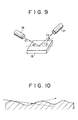
- JP-A-60-82840 discloses a RHEED/TRAXS analysis method in which, as shown in Fig. 9 of the accompanying drawings, the characteristic X-rays (fluorescent X-rays) Cx emitted from a surface of a sample 15 excited by an electron beam Ei with an incident angle a from an electron gun 16 are detected by a detector 17 at the total reflection angle ⁇ .
- This method is advantageous because of a high detection sensitivity but has a problem because the X-ray penetration depth is not sufficiently small (30-50 ⁇ ) and because the analysis is unable to be performed when the surface to be detected is not smooth.
- the present invention has been made from a consideration of the problems of the prior art.
- a method of determining the atoms constituting a surface of a solid sample comprising the steps of:
- the electron beam is impinged on the island-like deposits rather than on the sample.
- the island-like deposits serve to function as an X-ray source.
- the fluorescent X-rays emitted from the island-like deposits are impinged on a surface of the sample.
- the critical angle for total reflection of the fluorescent X-rays reflected on the surface is measured.
- the effective penetration depth of the evanescent wave is in the range of about 10-20 ⁇ , so that the outermost atomic layer can be identified with high resolution, irrespective of the incident angle of the electron beam.
- the X-ray source is small in size and is present adjacent to the surface to be measured, the surface roughness of the sample does not adversely affect the identification of the surface atomic layer thereof.
- the present invention provides a device for determining the surface atomic layer of a solid sample, comprising:
- a vessel defining therewithin an airtight chamber 1a and having an evacuation port connected to a vacuum pump (not shown) for maintaining the chamber 1a in a vacuum state.
- a sample holder 4a Disposed in the chamber 1a is a sample holder 4a for securing a sample 4 to be measured at a predetermined orientation.
- Heater means 3 is disposed in the chamber 1a for, heating the sample 4.
- Designated as 11 is a substance, e.g. gold, silver or copper, capable of generating fluorescent X-rays upon being energized by an electron beam.
- an electron gun 5 Disposed also in the chamber 1a is an electron gun 5 which may be primarily, electron beam source used in the conventional RHEED method.
- the electron gun 5 is used for forming island-like deposits 11a of the substance 11 on the sample 4 as well as for exciting the island-like deposits 11a on the sample 4 so as to emit fluorescent X-rays therefrom.
- the island state of the deposits 11a formed on the sample 4 is confirmed by a RHEED screen 10.
- the measuring means 12 may be a conventional one as used in TRAXS and includes a Si(Li) energy dispersive X-ray detector 7 arranged to receive the exiting X-rays through a slit 6 and Be windows 6a and 6b, a spectrum analyzer 8 and memorizing and display means 9.
- the orientation angle ⁇ t of the detector 7 relative to the surface of the sample 4 may be changed around the critical angle ⁇ c for total reflection.
- the substance 11 when the substance 11 is excited with the electron gun 5, while heating the sample 4 with the heater 3 at, for example, 200-300°C and while maintaining the chamber 1a in vacuum state, the substance 11 deposits on a surface of the sample 4 secured in the vacuum chamber 1a by the holder 4a, thereby to form, as shown in Fig. 2 island-like deposits 11a randomly distributed on the sample 4 and each surrounded by non-coated surface of the sample 4.
- the diameter of each of the deposits 11a is preferably 5-1,000 nm, more preferably 10-100 nm.
- the electron beam is then impinged upon the island-like deposits 11a so that the fluorescent X-rays are emitted therefrom in all directions around the islands 11a.
- the island state of the deposits 11a may be confirmed by a pattern formed on the RHEED screen 10. As shown in Fig. 3, the incoming X-rays I i impinge on the surface of the sample 4 and encounter the total reflection on the surface when the incident angle ⁇ i is smaller than the critical angle ⁇ c .
- the surface atomic layer can be identified by measuring the critical angle ⁇ c for total reflection.
- the intensity of the exiting X-rays I e at exiting angle ⁇ t is detected by the detector 7 (Fig. 1) while changing the angle of the direction of the detector 7 relative to the sample 4.
- the outputs from the detector 7 are analyzed in the spectrum analyzer 8 and the results are memorized and displayed in the device 9, whereupon the critical angle for total reflection ⁇ c is determined.
- SrTiO 3 (001) perovskite single crystal has a layer structure in which TiO 2 (2 ⁇ ) and SrO (2 ⁇ ) atomic layers are alternately stacked. It is known that the surface layer depends on the surface treatment. For example, a SrTiO 3 surface annealed shows two kinds of termination layers as shown in Fig. 5.
- a SrTiO 3 sample annealed at 1,000°C for 10 hours in 1 atm (1 bar) oxygen was measured for the identification of the surface atomic layer by the method according to the present invention.
- the sample was set in a vacuum chamber of a RHEED-TRAXS device as shown in Fig. 1 and Au deposits were formed in situ on a surface of the sample by electron beam deposition using the primary electron beam of the RHEED.
- the RHEED and high resolution scanning electron microscopy were used to confirm the island state of the Au deposits.
- the slit with a 0.2 mm separation insured an angular resolution of 0.05°.
- intensity variation of an exiting X-ray As a function of the exit angle ⁇ t , the detector was moved on a circle centered at the sample surface in the vertical plane within 0-3°. The results are shown in Fig. 6. Two peaks ⁇ 1 and ⁇ 2 representing the critical angles for total reflection were observed.
- the results observed by the present method identified that the annealed SrTiO 3 surface was mainly terminated with a TiO 2 plane (giving the peak ⁇ 1 ) with a small portion covered by a SrO plane (giving the peak ⁇ 2 ).
- ⁇ c (degree) ⁇ (g/cm 3 ) Found ⁇ 1 1.10 ⁇ 2 1.34 Calculated TiO 2 1.13 4.46 ( ⁇ layer) SrO 1.29 5.80 ( ⁇ layer) SrTiO 3 1.21 5.13 ( ⁇ unit)
- NBCO NdBa 2 Cu 3 O x (6 ⁇ x ⁇ 7)
- a SrTiO 3 substrate by a laser ablation process.
- the structure of the laminate is schematically shown in Fig. 7.
- the surface atomic layer of the NBCO film was identified by a method similar to that of Example 1. Ag was used to form island-like deposits. The results are shown in Fig. 8 and Table 2.
- Table 2 shows the values of ⁇ 1 observed from Fig. 8 and calculated critical angle ⁇ c values. Also shown in Table 1 are values of ⁇ layer calculated for respective atomic layers, and ⁇ unit for bulk NdBa 2 Cu 3 O x .
- the surface atomic layer of the NBCO film is CuO or Cu 2 O. This result is in conformity with that obtained by atomic force microscope (AFM).
Landscapes
- Chemical & Material Sciences (AREA)
- Analytical Chemistry (AREA)
- Physics & Mathematics (AREA)
- Health & Medical Sciences (AREA)
- Life Sciences & Earth Sciences (AREA)
- Biochemistry (AREA)
- General Health & Medical Sciences (AREA)
- General Physics & Mathematics (AREA)
- Immunology (AREA)
- Pathology (AREA)
- Analysing Materials By The Use Of Radiation (AREA)
Description
- This invention relates to a method of determining the surface atomic layer of a solid sample by a reflection high energy electron diffraction (RHEED) method combined with (TRAXS) total reflection angle X-ray spectroscopy.
- In the conventional RHEED method, the characteristic X-rays emitted from a surface of a sample when an electron beam is impinged thereon are detected to determine the elements constituting the surface of the sample. One problem of the RHEED method is a low measurement sensitivity attributed to the low intensity of the characteristic X-rays.
- JP-A-60-82840 discloses a RHEED/TRAXS analysis method in which, as shown in Fig. 9 of the accompanying drawings, the characteristic X-rays (fluorescent X-rays) Cx emitted from a surface of a
sample 15 excited by an electron beam Ei with an incident angle a from anelectron gun 16 are detected by adetector 17 at the total reflection angle β. This method is advantageous because of a high detection sensitivity but has a problem because the X-ray penetration depth is not sufficiently small (30-50 Å) and because the analysis is unable to be performed when the surface to be detected is not smooth. - More particularly, when the conventional RHEED/TRAXS analysis is applied to, for example, (100) plane of a perovskite crystal of ABO3 in which the atomic layer containing the element A and the atomic layer containing the element B are alternately stacked, not only the outermost atomic layer but also the inner adjacent layer are simultaneously energized with the electron beam, so that it is impossible to identify the outermost atomic layer. In order to minimize the penetration depth as small as possible, therefore, it is necessary to set the incident angle α at about 0.1-1 radian. In this case, when the sample has a rough surface, it is impossible to obtain the critical angle for total reflection at certain positions, as shown in Fig. 10 of the accompanying drawings.
- The present invention has been made from a consideration of the problems of the prior art.
- There is provided in accordance with the present invention, a method of determining the atoms constituting a surface of a solid sample, comprising the steps of:
- forming, on a surface of said sample, island-like deposits of a substance capable of generating fluorescent X-rays upon being energized by an electron beam, such that said island-like deposits are surrounded by a non-coated surface of said sample;
- energizing said deposits with an electron beam so that fluorescent X-rays are emitted therefrom and reflected on said non-coated surface;
- measuring the critical angle for total reflection c of the fluorescent X-rays reflected on said non-coated surface of said sample; and
- identifying from the measured critical angle, the atoms constituting the non-coated surface.
-
- In the method of the present invention, the electron beam is impinged on the island-like deposits rather than on the sample. The island-like deposits serve to function as an X-ray source. Thus, the fluorescent X-rays emitted from the island-like deposits are impinged on a surface of the sample. The critical angle for total reflection of the fluorescent X-rays reflected on the surface is measured. By this expedient, the effective penetration depth of the evanescent wave is in the range of about 10-20 Å, so that the outermost atomic layer can be identified with high resolution, irrespective of the incident angle of the electron beam. Further, since the X-ray source is small in size and is present adjacent to the surface to be measured, the surface roughness of the sample does not adversely affect the identification of the surface atomic layer thereof.
- In another aspect, the present invention provides a device for determining the surface atomic layer of a solid sample, comprising:
- a vessel defining an airtight chamber therewithin;
- evacuation means for maintaining said chamber in a vacuum state;
- a holder disposed in said chamber for securing said sample at a predetermined orientation;
- heater means for heating said sample, so that when a substance capable of generating fluorescent X-rays upon being energized by an electron beam is placed in said chamber and heated under vacuum, island-like deposits may be formed on a surface of said sample with each deposit being surrounded by a non-coated surface of said sample;
- an electron beam gun for impinging electron beams either on said substance or on said islands-like deposits on said sample; and
- means for measuring the critical angle for total reflection of the fluorescent X-rays reflected on said non-coated surface.
-
- Preferred embodiments of the invention will now be described with reference to the accompanying drawings, in which:
- Fig. 1 is a schematic illustration of a surface element detecting device according to the present invention;
- Fig. 2 is a sectional view schematically illustrating island-like deposits on a sample to be measured;
- Fig. 3 is a sectional view, similar to Fig. 2, showing the function of the island-like deposits;
- Fig. 4 is a schematic illustration of the atomic layer structure of SrTiO3;
- Fig. 5 is a schematic illustration of the microscopic surface structure of SrTiO3;
- Fig. 6 shows the exit angle dependency of an exiting X-ray (Au Mα X-ray) obtained in the surface layer identification of SrTiO3 in Example 1;
- Fig. 7 is a schematic illustration of the microscopic surface structure of NdBa2Cu3Ox;
- Fig. 8 shows the exit angle dependency of an exiting X-ray (Ag Lα X-ray) obtained in the surface layer identification of NdBa2Cu3Ox in Example 2;
- Fig. 9 is a schematic illustration of the known RHEED/TRAXS analysis method; and
- Fig. 10 is a schematic illustration of the RHEED/TRAXS method applied to the measurement of a roughed surface.
-
- Referring now to Fig. 1, designated as 1 is a vessel defining therewithin an airtight chamber 1a and having an evacuation port connected to a vacuum pump (not shown) for maintaining the chamber 1a in a vacuum state. Disposed in the chamber 1a is a sample holder 4a for securing a
sample 4 to be measured at a predetermined orientation. Heater means 3 is disposed in the chamber 1a for, heating thesample 4. - Designated as 11 is a substance, e.g. gold, silver or copper, capable of generating fluorescent X-rays upon being energized by an electron beam.
- Disposed also in the chamber 1a is an
electron gun 5 which may be primarily, electron beam source used in the conventional RHEED method. Theelectron gun 5 is used for forming island-like deposits 11a of the substance 11 on thesample 4 as well as for exciting the island-like deposits 11a on thesample 4 so as to emit fluorescent X-rays therefrom. The island state of the deposits 11a formed on thesample 4 is confirmed by aRHEED screen 10. - Designated generally as 12 is means for measuring the critical angle for total reflection of the fluorescent X-rays reflected on a surface of the
sample 4. The measuring means 12 may be a conventional one as used in TRAXS and includes a Si(Li) energydispersive X-ray detector 7 arranged to receive the exiting X-rays through a slit 6 and Bewindows spectrum analyzer 8 and memorizing and display means 9. The orientation angle t of thedetector 7 relative to the surface of thesample 4 may be changed around the critical angle c for total reflection. - With the foregoing structure of the surface atomic layer identification device, when the substance 11 is excited with the
electron gun 5, while heating thesample 4 with theheater 3 at, for example, 200-300°C and while maintaining the chamber 1a in vacuum state, the substance 11 deposits on a surface of thesample 4 secured in the vacuum chamber 1a by the holder 4a, thereby to form, as shown in Fig. 2 island-like deposits 11a randomly distributed on thesample 4 and each surrounded by non-coated surface of thesample 4. The diameter of each of the deposits 11a is preferably 5-1,000 nm, more preferably 10-100 nm. - The electron beam is then impinged upon the island-like deposits 11a so that the fluorescent X-rays are emitted therefrom in all directions around the islands 11a. In this case, the island state of the deposits 11a may be confirmed by a pattern formed on the
RHEED screen 10. As shown in Fig. 3, the incoming X-rays Ii impinge on the surface of thesample 4 and encounter the total reflection on the surface when the incident angle i is smaller than the critical angle c. Since the critical angle c for total reflection is given by:sample 4 and E is the energy (KeV) of the X-rays, the surface atomic layer can be identified by measuring the critical angle c for total reflection. Thus, the intensity of the exiting X-rays Ie at exiting angle t is detected by the detector 7 (Fig. 1) while changing the angle of the direction of thedetector 7 relative to thesample 4. The outputs from thedetector 7 are analyzed in thespectrum analyzer 8 and the results are memorized and displayed in thedevice 9, whereupon the critical angle for total reflection c is determined. - The following examples will further illustrate the present invention.
- As schematically shown in Fig. 4, SrTiO3 (001) perovskite single crystal has a layer structure in which TiO2 (2Å) and SrO (2Å) atomic layers are alternately stacked. It is known that the surface layer depends on the surface treatment. For example, a SrTiO3 surface annealed shows two kinds of termination layers as shown in Fig. 5.
- Thus, a SrTiO3 sample annealed at 1,000°C for 10 hours in 1 atm (1 bar) oxygen was measured for the identification of the surface atomic layer by the method according to the present invention. The sample was set in a vacuum chamber of a RHEED-TRAXS device as shown in Fig. 1 and Au deposits were formed in situ on a surface of the sample by electron beam deposition using the primary electron beam of the RHEED. The RHEED and high resolution scanning electron microscopy were used to confirm the island state of the Au deposits. A Si(Li) energy-dispersive X-ray detector with a resolution of 165 eV, located at 45° from the direction of the primary electron beam, was combined with the vacuum chamber through a slit and Be windows. The slit with a 0.2 mm separation insured an angular resolution of 0.05°. In order to observe intensity variation of an exiting X-ray (Au Mα X-ray) as a function of the exit angle t, the detector was moved on a circle centered at the sample surface in the vertical plane within 0-3°. The results are shown in Fig. 6. Two peaks 1 and 2 representing the critical angles for total reflection were observed.
- Table 1 below shows the values of 1 and 2 observed from Fig. 6 and calculated critical angle c for Au Mα X-ray (E = 2.12 KeV). Also shown in Table 1 are values of ρlayer calculated for TiO2 and SrO layers, and ρunit for bulk SrTiO3. As will be appreciated from Table 1, the values of 1 and 2 are much closer to the calculated c values based on ρlayer for TiO2 and SrO layers than that based on ρunit for bulk SrTiO3. Namely, the results observed by the present method identified that the annealed SrTiO3 surface was mainly terminated with a TiO2 plane (giving the peak 1) with a small portion covered by a SrO plane (giving the peak 2).
c (degree) ρ (g/cm3) Found 1 1.10 2 1.34 Calculated TiO2 1.13 4.46 (ρlayer) SrO 1.29 5.80 (ρlayer) SrTiO3 1.21 5.13 (ρunit) - An NBCO (NdBa2Cu3Ox (6 < x ≤ 7)) film having a thickness of 100 nm was laminated on a SrTiO3 substrate by a laser ablation process. The structure of the laminate is schematically shown in Fig. 7. The surface atomic layer of the NBCO film was identified by a method similar to that of Example 1. Ag was used to form island-like deposits. The results are shown in Fig. 8 and Table 2.
- Fig. 8 shows the intensity variation of Ag Lα X-ray (E = 2.986 KeV) emitted from the Ag adlayer deposited on the NBCO film surface with the exit angle t. Table 2 shows the values of 1 observed from Fig. 8 and calculated critical angle c values. Also shown in Table 1 are values of ρlayer calculated for respective atomic layers, and ρunit for bulk NdBa2Cu3Ox. As will be appreciated from Table 2, the surface atomic layer of the NBCO film is CuO or Cu2O. This result is in conformity with that obtained by atomic force microscope (AFM).
c (degree) ρ (g/cm3) Found 1 0.83 Calculated Nd 1.14 8.06 (ρlayer) BaO 1.09 8.75 (ρlayer) CuO 0.77 4.53 (ρlayer) Cu2O 0.91 5.44 (ρlayer) NdBa2Cu3Ox 0.99 6.70 (ρunit) BaCuO2 0.92 5.82 (ρunit)
Claims (6)
- A method of determining the atoms constituting a surface of a solid sample (4), comprising the steps of:forming, on a surface of said sample, island-like deposits (11a) of a substance (11) capable of generating fluorescent X-rays upon being energized by an electron beam, such that said island-like deposits are surrounded by a non-coated surface of said sample;energizing said deposits with an electron beam so that fluorescent X-rays are emitted therefrom and reflected on said non-coated surface;measuring the critical angle for total reflection (c) of the fluorescent X-rays reflected on said non-coated surface of said sample; andidentifying from the measured critical angle, the atoms constituting the non-coated surface.
- A method as claimed in claim 1, wherein said substance (11) is gold, silver or copper.
- A method as claimed in claim 1 or claim 2, wherein said deposits (11a) each have a diameter of 5-1,000 nm.
- A method as claimed in claim 3, wherein said deposits (11a) each have a diameter of 10-100 nm.
- A device for determining the surface atomic layer of a solid sample, comprising,
a vessel (1) defining an airtight chamber (1a) therewithin;
evacuation means for maintaining said chamber in a vacuum state;
a holder (4a) disposed in said chamber for securing said sample (4) at a predetermined orientation;
heater means (3) for heating said sample, so that when a substance (11) capable of generating fluorescent X-rays upon being energized by an electron beam is placed in said chamber and heated under vacuum, island-like deposits (11a) may be formed on a surface of said sample with each deposit being surrounded by a non-coated surface of said sample;
an electron beam gun (5) for impinging electron beams either on said substance or on said islands-like deposits on said sample; and
means (12) for measuring the critical angle for total reflection of the fluorescent X-rays reflected on said non-coated surface. - A device as claimed in claim 5, further comprising means (10) for detecting the island state of said deposits.
Applications Claiming Priority (3)
| Application Number | Priority Date | Filing Date | Title |
|---|---|---|---|
| JP5918495 | 1995-03-17 | ||
| JP59184/95 | 1995-03-17 | ||
| JP05918495A JP3165615B2 (en) | 1995-03-17 | 1995-03-17 | Surface elemental analysis method and device |
Publications (3)
| Publication Number | Publication Date |
|---|---|
| EP0732725A2 EP0732725A2 (en) | 1996-09-18 |
| EP0732725A3 EP0732725A3 (en) | 1997-12-29 |
| EP0732725B1 true EP0732725B1 (en) | 2003-05-14 |
Family
ID=13106076
Family Applications (1)
| Application Number | Title | Priority Date | Filing Date |
|---|---|---|---|
| EP96301728A Expired - Lifetime EP0732725B1 (en) | 1995-03-17 | 1996-03-14 | Method for identifying surface atoms of solid sample and apparatus therefor |
Country Status (4)
| Country | Link |
|---|---|
| US (1) | US5635716A (en) |
| EP (1) | EP0732725B1 (en) |
| JP (1) | JP3165615B2 (en) |
| DE (1) | DE69628067T2 (en) |
Families Citing this family (8)
| Publication number | Priority date | Publication date | Assignee | Title |
|---|---|---|---|---|
| JP3165615B2 (en) | 1995-03-17 | 2001-05-14 | 財団法人国際超電導産業技術研究センター | Surface elemental analysis method and device |
| JP3649823B2 (en) | 1996-09-17 | 2005-05-18 | 株式会社トプコン | Organic matter analyzer |
| JP2004500542A (en) * | 1998-09-03 | 2004-01-08 | ケーエルエー−テンカー テクノロジィース コーポレイション | Chemical analysis of defects using electron appearance spectroscopy |
| US6180456B1 (en) * | 1999-02-17 | 2001-01-30 | International Business Machines Corporation | Triple polysilicon embedded NVRAM cell and method thereof |
| JP2003050115A (en) * | 2001-08-07 | 2003-02-21 | Seiko Instruments Inc | X-ray thickness gauge |
| US7095822B1 (en) * | 2004-07-28 | 2006-08-22 | Xradia, Inc. | Near-field X-ray fluorescence microprobe |
| WO2023145101A1 (en) | 2022-01-31 | 2023-08-03 | キヤノンアネルバ株式会社 | Inspection device and inspection method |
| JP2025532970A (en) * | 2022-10-07 | 2025-10-03 | シランナ・ユー・ブイ・テクノロジーズ・プライベート・リミテッド | Surface characterization of materials using cathodoluminescence |
Family Cites Families (7)
| Publication number | Priority date | Publication date | Assignee | Title |
|---|---|---|---|---|
| BE793444A (en) * | 1971-12-29 | 1973-04-16 | Aquitaine Petrole | X-RAY SPECTROMETRIC ANALYSIS METHOD AND EQUIPMENT |
| JPH0676975B2 (en) * | 1984-09-26 | 1994-09-28 | 新技術事業団 | Observation method of surface atomic arrangement structure |
| US4746571A (en) * | 1986-08-01 | 1988-05-24 | Wisconsin Alumni Research Foundation | X-ray detector efficiency standard for electron microscopes |
| DE69024485T2 (en) * | 1990-06-04 | 1996-05-30 | Kazuya Masu | Method for observing a microscopic surface structure |
| EP0523566B1 (en) * | 1991-07-11 | 2001-11-21 | International Superconductivity Technology Center | Apparatus for solid surface analysis using x-ray spectroscopy |
| JPH0682840A (en) * | 1992-09-07 | 1994-03-25 | Toyota Central Res & Dev Lab Inc | Antidazzle mirror |
| JP3165615B2 (en) | 1995-03-17 | 2001-05-14 | 財団法人国際超電導産業技術研究センター | Surface elemental analysis method and device |
-
1995
- 1995-03-17 JP JP05918495A patent/JP3165615B2/en not_active Expired - Fee Related
-
1996
- 1996-03-13 US US08/614,678 patent/US5635716A/en not_active Expired - Fee Related
- 1996-03-14 EP EP96301728A patent/EP0732725B1/en not_active Expired - Lifetime
- 1996-03-14 DE DE69628067T patent/DE69628067T2/en not_active Expired - Lifetime
Also Published As
| Publication number | Publication date |
|---|---|
| EP0732725A2 (en) | 1996-09-18 |
| EP0732725A3 (en) | 1997-12-29 |
| DE69628067T2 (en) | 2004-04-01 |
| DE69628067D1 (en) | 2003-06-18 |
| JP3165615B2 (en) | 2001-05-14 |
| US5635716A (en) | 1997-06-03 |
| JPH08261960A (en) | 1996-10-11 |
Similar Documents
| Publication | Publication Date | Title |
|---|---|---|
| US5481109A (en) | Surface analysis method and apparatus for carrying out the same | |
| US5280176A (en) | X-ray photoelectron emission spectrometry system | |
| US4599741A (en) | System for local X-ray excitation by monochromatic X-rays | |
| US5635716A (en) | Method for identifying surface atoms of solid sample and apparatus therefor | |
| JPWO1994008232A1 (en) | Surface analysis method and apparatus | |
| JPH07325052A (en) | Scanning and high-resolution electronic spectroscopy and image pickup device | |
| WO2001023873A1 (en) | X-ray microanalyzer for thin films | |
| EP0388872B1 (en) | Method for examination of surface structures | |
| US6577705B1 (en) | Combinatorial material analysis using X-ray capillary optics | |
| US6529578B1 (en) | X-ray condenser and x-ray apparatus | |
| GB2165353A (en) | Method of observing the arrangement of atoms on a surface and apparatus therefor | |
| US6628748B2 (en) | Device and method for analyzing atomic and/or molecular elements by means of wavelength dispersive X-ray spectrometric devices | |
| JPH08327514A (en) | Preparation of sample for transmission electron microscope and device therefor | |
| US5739542A (en) | X-ray analyzing | |
| Houdy et al. | Performances Of CW Multilayers As Soft X-Rays Optics: High Reflectivity In The Range 2d= 60 to 100 A | |
| Nakashima et al. | Characterization of ion implanted and laser annealed polycrystalline Si by a Raman microprobe | |
| WO1995023963A1 (en) | X-ray spectrometer with a grazing take-off angle | |
| JPH0712716A (en) | Infrared ray absorption reinforcing spectrometer | |
| Dai et al. | Raman intensity enhancement of the Si peak by CdS thin films | |
| JPH06191995A (en) | Method for manufacturing oxide superconducting thin film | |
| EP0646786A1 (en) | Improved ion scattering spectroscopy and apparatus for the same | |
| Drummond et al. | Methodology, performance, and application of an imaging x‐ray photoelectron spectrometer | |
| Ziyuan Liu et al. | Measurement of glancing incidence-exit X-ray scattering in reflection high energy electron diffraction and total-reflection-angle X-ray spectroscopy system | |
| Cricenti et al. | IR‐SNOM on lithium fluoride films with regular arrays based on colour centres | |
| JP3217871B2 (en) | X-ray analyzer and total reflection X-ray fluorescence analyzer |
Legal Events
| Date | Code | Title | Description |
|---|---|---|---|
| PUAI | Public reference made under article 153(3) epc to a published international application that has entered the european phase |
Free format text: ORIGINAL CODE: 0009012 |
|
| AK | Designated contracting states |
Kind code of ref document: A2 Designated state(s): DE FR GB |
|
| PUAL | Search report despatched |
Free format text: ORIGINAL CODE: 0009013 |
|
| AK | Designated contracting states |
Kind code of ref document: A3 Designated state(s): DE FR GB |
|
| RHK1 | Main classification (correction) |
Ipc: G01N 23/225 |
|
| 17P | Request for examination filed |
Effective date: 19980220 |
|
| 17Q | First examination report despatched |
Effective date: 20000713 |
|
| GRAH | Despatch of communication of intention to grant a patent |
Free format text: ORIGINAL CODE: EPIDOS IGRA |
|
| GRAH | Despatch of communication of intention to grant a patent |
Free format text: ORIGINAL CODE: EPIDOS IGRA |
|
| GRAA | (expected) grant |
Free format text: ORIGINAL CODE: 0009210 |
|
| AK | Designated contracting states |
Designated state(s): DE FR GB |
|
| REG | Reference to a national code |
Ref country code: GB Ref legal event code: FG4D |
|
| REF | Corresponds to: |
Ref document number: 69628067 Country of ref document: DE Date of ref document: 20030618 Kind code of ref document: P |
|
| ET | Fr: translation filed | ||
| PLBE | No opposition filed within time limit |
Free format text: ORIGINAL CODE: 0009261 |
|
| STAA | Information on the status of an ep patent application or granted ep patent |
Free format text: STATUS: NO OPPOSITION FILED WITHIN TIME LIMIT |
|
| 26N | No opposition filed |
Effective date: 20040217 |
|
| REG | Reference to a national code |
Ref country code: GB Ref legal event code: 732E |
|
| REG | Reference to a national code |
Ref country code: FR Ref legal event code: TQ |
|
| PGFP | Annual fee paid to national office [announced via postgrant information from national office to epo] |
Ref country code: FR Payment date: 20110317 Year of fee payment: 16 |
|
| PGFP | Annual fee paid to national office [announced via postgrant information from national office to epo] |
Ref country code: GB Payment date: 20110309 Year of fee payment: 16 Ref country code: DE Payment date: 20110309 Year of fee payment: 16 |
|
| GBPC | Gb: european patent ceased through non-payment of renewal fee |
Effective date: 20120314 |
|
| REG | Reference to a national code |
Ref country code: FR Ref legal event code: ST Effective date: 20121130 |
|
| REG | Reference to a national code |
Ref country code: DE Ref legal event code: R119 Ref document number: 69628067 Country of ref document: DE Effective date: 20121002 |
|
| PG25 | Lapsed in a contracting state [announced via postgrant information from national office to epo] |
Ref country code: FR Free format text: LAPSE BECAUSE OF NON-PAYMENT OF DUE FEES Effective date: 20120402 Ref country code: GB Free format text: LAPSE BECAUSE OF NON-PAYMENT OF DUE FEES Effective date: 20120314 |
|
| PG25 | Lapsed in a contracting state [announced via postgrant information from national office to epo] |
Ref country code: DE Free format text: LAPSE BECAUSE OF NON-PAYMENT OF DUE FEES Effective date: 20121002 |