EP0731576A2 - Gain equalization using monolithic planar waveguide grating multiplexer and demultiplexer - Google Patents
Gain equalization using monolithic planar waveguide grating multiplexer and demultiplexer Download PDFInfo
- Publication number
- EP0731576A2 EP0731576A2 EP96102043A EP96102043A EP0731576A2 EP 0731576 A2 EP0731576 A2 EP 0731576A2 EP 96102043 A EP96102043 A EP 96102043A EP 96102043 A EP96102043 A EP 96102043A EP 0731576 A2 EP0731576 A2 EP 0731576A2
- Authority
- EP
- European Patent Office
- Prior art keywords
- optical
- demultiplexer
- multiplexer
- channels
- equalizer
- Prior art date
- Legal status (The legal status is an assumption and is not a legal conclusion. Google has not performed a legal analysis and makes no representation as to the accuracy of the status listed.)
- Granted
Links
Images
Classifications
-
- H—ELECTRICITY
- H04—ELECTRIC COMMUNICATION TECHNIQUE
- H04B—TRANSMISSION
- H04B10/00—Transmission systems employing electromagnetic waves other than radio-waves, e.g. infrared, visible or ultraviolet light, or employing corpuscular radiation, e.g. quantum communication
- H04B10/29—Repeaters
- H04B10/291—Repeaters in which processing or amplification is carried out without conversion of the main signal from optical form
- H04B10/293—Signal power control
- H04B10/294—Signal power control in a multiwavelength system, e.g. gain equalisation
-
- G—PHYSICS
- G02—OPTICS
- G02B—OPTICAL ELEMENTS, SYSTEMS OR APPARATUS
- G02B6/00—Light guides; Structural details of arrangements comprising light guides and other optical elements, e.g. couplings
- G02B6/10—Light guides; Structural details of arrangements comprising light guides and other optical elements, e.g. couplings of the optical waveguide type
- G02B6/12—Light guides; Structural details of arrangements comprising light guides and other optical elements, e.g. couplings of the optical waveguide type of the integrated circuit kind
- G02B6/12007—Light guides; Structural details of arrangements comprising light guides and other optical elements, e.g. couplings of the optical waveguide type of the integrated circuit kind forming wavelength selective elements, e.g. multiplexer, demultiplexer
- G02B6/12009—Light guides; Structural details of arrangements comprising light guides and other optical elements, e.g. couplings of the optical waveguide type of the integrated circuit kind forming wavelength selective elements, e.g. multiplexer, demultiplexer comprising arrayed waveguide grating [AWG] devices, i.e. with a phased array of waveguides
- G02B6/12011—Light guides; Structural details of arrangements comprising light guides and other optical elements, e.g. couplings of the optical waveguide type of the integrated circuit kind forming wavelength selective elements, e.g. multiplexer, demultiplexer comprising arrayed waveguide grating [AWG] devices, i.e. with a phased array of waveguides characterised by the arrayed waveguides, e.g. comprising a filled groove in the array section
-
- G—PHYSICS
- G02—OPTICS
- G02B—OPTICAL ELEMENTS, SYSTEMS OR APPARATUS
- G02B6/00—Light guides; Structural details of arrangements comprising light guides and other optical elements, e.g. couplings
- G02B6/10—Light guides; Structural details of arrangements comprising light guides and other optical elements, e.g. couplings of the optical waveguide type
- G02B6/12—Light guides; Structural details of arrangements comprising light guides and other optical elements, e.g. couplings of the optical waveguide type of the integrated circuit kind
- G02B6/12007—Light guides; Structural details of arrangements comprising light guides and other optical elements, e.g. couplings of the optical waveguide type of the integrated circuit kind forming wavelength selective elements, e.g. multiplexer, demultiplexer
-
- G—PHYSICS
- G02—OPTICS
- G02B—OPTICAL ELEMENTS, SYSTEMS OR APPARATUS
- G02B6/00—Light guides; Structural details of arrangements comprising light guides and other optical elements, e.g. couplings
- G02B6/10—Light guides; Structural details of arrangements comprising light guides and other optical elements, e.g. couplings of the optical waveguide type
- G02B6/12—Light guides; Structural details of arrangements comprising light guides and other optical elements, e.g. couplings of the optical waveguide type of the integrated circuit kind
- G02B6/12007—Light guides; Structural details of arrangements comprising light guides and other optical elements, e.g. couplings of the optical waveguide type of the integrated circuit kind forming wavelength selective elements, e.g. multiplexer, demultiplexer
- G02B6/12009—Light guides; Structural details of arrangements comprising light guides and other optical elements, e.g. couplings of the optical waveguide type of the integrated circuit kind forming wavelength selective elements, e.g. multiplexer, demultiplexer comprising arrayed waveguide grating [AWG] devices, i.e. with a phased array of waveguides
- G02B6/12019—Light guides; Structural details of arrangements comprising light guides and other optical elements, e.g. couplings of the optical waveguide type of the integrated circuit kind forming wavelength selective elements, e.g. multiplexer, demultiplexer comprising arrayed waveguide grating [AWG] devices, i.e. with a phased array of waveguides characterised by the optical interconnection to or from the AWG devices, e.g. integration or coupling with lasers or photodiodes
- G02B6/12021—Comprising cascaded AWG devices; AWG multipass configuration; Plural AWG devices integrated on a single chip
-
- H—ELECTRICITY
- H04—ELECTRIC COMMUNICATION TECHNIQUE
- H04B—TRANSMISSION
- H04B10/00—Transmission systems employing electromagnetic waves other than radio-waves, e.g. infrared, visible or ultraviolet light, or employing corpuscular radiation, e.g. quantum communication
- H04B10/25—Arrangements specific to fibre transmission
- H04B10/2507—Arrangements specific to fibre transmission for the reduction or elimination of distortion or dispersion
- H04B10/25073—Arrangements specific to fibre transmission for the reduction or elimination of distortion or dispersion using spectral equalisation, e.g. spectral filtering
-
- H—ELECTRICITY
- H04—ELECTRIC COMMUNICATION TECHNIQUE
- H04B—TRANSMISSION
- H04B10/00—Transmission systems employing electromagnetic waves other than radio-waves, e.g. infrared, visible or ultraviolet light, or employing corpuscular radiation, e.g. quantum communication
- H04B10/25—Arrangements specific to fibre transmission
- H04B10/2581—Multimode transmission
-
- H—ELECTRICITY
- H04—ELECTRIC COMMUNICATION TECHNIQUE
- H04J—MULTIPLEX COMMUNICATION
- H04J14/00—Optical multiplex systems
- H04J14/02—Wavelength-division multiplex systems
- H04J14/0221—Power control, e.g. to keep the total optical power constant
-
- H—ELECTRICITY
- H04—ELECTRIC COMMUNICATION TECHNIQUE
- H04B—TRANSMISSION
- H04B2210/00—Indexing scheme relating to optical transmission systems
- H04B2210/25—Distortion or dispersion compensation
- H04B2210/258—Distortion or dispersion compensation treating each wavelength or wavelength band separately
Definitions
- the present invention relates to the gain equalization for optical fibers transmitting optical signals at multiple wavelengths.
- a metropolitan area network or wide area network (MAN/WAN) using WDMA/WDM has the potential near-far problem where the optical signals originating from different locations experience different attenuation.
- fibers and optical amplifiers used in such a network also have nonflat transmission spectra and thus different wavelengths experience different gain and attenuation even though they travel through the same physical path.
- the nonuniform gain of the amplifiers yields different gain factors for different signals distributed across its spectrum. The problem becomes severe as many optical amplifiers are cascaded together. This effect reduces the system margin and may exceed the dynamic range of the detectors. Gain equalization is thus needed.
- Gain equalization using fiber grating embedded in the Er 3 + fiber amplifier was proposed in [1].
- a two-stage amplifier with offset gain peaks was proposed in [2] to dynamically equalize (by means of pump power) the optical signal power among different channels in a WDMA system.
- This scheme has a very limited equalized bandwidth of approximately 2.5 nm.
- Gain equalization can also be achieved through controlling the transmission spectra of the optical filters. Using this principle, an equalized 29-channel WDM system spanning 7 nm was demonstrated using a Mach-Zehnder Interferometric filter [3] .
- AOTF acousto-optic tunable filter
- MAN/WAN Micropolitan Area Network/Wide Area Network
- this invention proposes an equalization scheme using planar gratings with metallic layers deposited on the waveguides to provide equalization.
- this invention is an optical equalizer for equalizing an optical signal having a number of wavelengths.
- This invention comprises an optical wavelength demultiplexer for demultiplexing the optical signal into a number of individual channels with each channel being centered at one of the wavelengths.
- This invention also comprises an optical multiplexer and a number of optical connections for connecting terminal of the multiplexers to terminals of demultiplexers. A plurality of metallic strips of predetermined lengths are then deposited on the optical connections so that the optical signal is equalized over the channels at the output channels of the optical multiplexer.
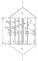
- FIG. 1 is a schematic illustration of the passive gain equalization device according to the invention.
- the planar grating (101 and 102) can function both as a demultiplexer (101) and as a multiplexer (102). Even though the planar grating (either the etched grating or the phase array) is the preferred structure for this invention, other structures which could resolve the incoming wavelengths into spatially different locations such as the Mach-Zehnder interferometer.
- demultiplexer 101 optical signals of different wavelengths will be diffracted by the grating and focused onto output waveguides designed for particular wavelengths.
- output waveguides designed for particular wavelengths.
- a set of designed wavelengths can be placed at the output waveguides and these wavelength can be combined into a single output through the grating.
- the invention is a monolithic structure consisting the demultiplexer and multiplexer back to back. Incoming wavelengths will be separated through different paths and combined together as a single output.
- the process of fabricating optical paths can be found, for example, in [5], which is hereby incorporated herein by reference.
- a metallic layer (104) will be deposited lithographically along the path of the waveguides (103) Transverse Electric Field (TE and Transverse Magnetic Field TM modes will be attenuated by the metallic layer) in which the optical signals needed to be attenuated.
- the deposition of a metal layer is typical in VLSI processing, and its technique is taught, for example, in [6], which is hereby incorporated herein by reference.
- the amount of required attenuation which can be calculated through system simulation of individual wavelength channels, is determined by the length of the metallic layer (L i ).
- planar waveguide grating based on InP, polymer or LiNbO3 substrate can be used.
- the attenuation of the waveguide is determined by the dimensions and the materials of the waveguide.
- the attenuation of the waveguide with metalization is ⁇ m9
- the attenuation of the waveguide without metalization is ⁇ .
- the equalized output power for each wavelength is equal to -18.33 dB and the total length of the waveguide is 3.33 cm.
- FIG. 1 illustrates the proposed device for gain equalization.
Landscapes
- Physics & Mathematics (AREA)
- Engineering & Computer Science (AREA)
- Computer Networks & Wireless Communication (AREA)
- Signal Processing (AREA)
- Microelectronics & Electronic Packaging (AREA)
- General Physics & Mathematics (AREA)
- Optics & Photonics (AREA)
- Electromagnetism (AREA)
- Spectroscopy & Molecular Physics (AREA)
- Optical Integrated Circuits (AREA)
- Optical Communication System (AREA)
- Cable Transmission Systems, Equalization Of Radio And Reduction Of Echo (AREA)
Abstract
Description
- The present invention relates to the gain equalization for optical fibers transmitting optical signals at multiple wavelengths.
- A metropolitan area network or wide area network (MAN/WAN) using WDMA/WDM has the potential near-far problem where the optical signals originating from different locations experience different attenuation. Furthermore, fibers and optical amplifiers used in such a network also have nonflat transmission spectra and thus different wavelengths experience different gain and attenuation even though they travel through the same physical path. The nonuniform gain of the amplifiers yields different gain factors for different signals distributed across its spectrum. The problem becomes severe as many optical amplifiers are cascaded together. This effect reduces the system margin and may exceed the dynamic range of the detectors. Gain equalization is thus needed.
- Most of the existing studies on gain equalization has been focused on equalizing the nonflat gain spectra of the optical amplifiers. Gain equalization using fiber grating embedded in the Er3 + fiber amplifier was proposed in [1]. A two-stage amplifier with offset gain peaks was proposed in [2] to dynamically equalize (by means of pump power) the optical signal power among different channels in a WDMA system. This scheme, however, has a very limited equalized bandwidth of approximately 2.5 nm. Gain equalization can also be achieved through controlling the transmission spectra of the optical filters. Using this principle, an equalized 29-channel WDM system spanning 7 nm was demonstrated using a Mach-Zehnder Interferometric filter [3] . Besides not having enough bandwidth, the Mach-Zehnder filter is very difficult to control for proper attenuation. An acousto-optic tunable filter (AOTF) has also been used to equalize gain spectra for a very wide transmission window [4]. Through the injection of multiple RF frequencies with each RF signal transmitting at a different magnitude, an arbitrary transmission characteristic can be established. The resolution of this scheme, however, is limited by the frequency of an AOTF.
- Therefore, there is a need for a low cost, wideband, passive, optical device to provide for optical communication over wide area and long haul communication networks.
- It is an object of this invention to provide a low cost, wide band passive optical equalization device to provide for optical equalization over long haul communication networks.
- It is the object of this invention to overcome the near-far problem due to the non-equal transmission spectra present in an optical MAN/WAN (Metropolitan Area Network/Wide Area Network) or in an optical long haul transmission system.
- It is another object to this invention to provide equalization in the bandwidth range of 30 nm to 50 nm.
- It is another object of this invention to maximize the equalized power at the output of the equalizer.
- It is yet another object of this invention to minimize the overall physical size of the equalizer.
- This invention proposes an equalization scheme using planar gratings with metallic layers deposited on the waveguides to provide equalization. Accordingly, this invention is an optical equalizer for equalizing an optical signal having a number of wavelengths. This invention comprises an optical wavelength demultiplexer for demultiplexing the optical signal into a number of individual channels with each channel being centered at one of the wavelengths. This invention also comprises an optical multiplexer and a number of optical connections for connecting terminal of the multiplexers to terminals of demultiplexers. A plurality of metallic strips of predetermined lengths are then deposited on the optical connections so that the optical signal is equalized over the channels at the output channels of the optical multiplexer.
- FIG. 1 is a schematic illustration of the passive gain equalization device according to the invention.
- In this invention, we propose a fully monolithic integrated photonic circuit based on SiO2/Si planar waveguide grating demultiplexer, as shown in FIG. 1.
- The planar grating (101 and 102) can function both as a demultiplexer (101) and as a multiplexer (102). Even though the planar grating (either the etched grating or the phase array) is the preferred structure for this invention, other structures which could resolve the incoming wavelengths into spatially different locations such as the Mach-Zehnder interferometer. With
demultiplexer 101, optical signals of different wavelengths will be diffracted by the grating and focused onto output waveguides designed for particular wavelengths. At a multiplexer (102), reversal of the situation holds. A set of designed wavelengths can be placed at the output waveguides and these wavelength can be combined into a single output through the grating. The invention is a monolithic structure consisting the demultiplexer and multiplexer back to back. Incoming wavelengths will be separated through different paths and combined together as a single output. The process of fabricating optical paths can be found, for example, in [5], which is hereby incorporated herein by reference. To equalize the various signals, a metallic layer (104) will be deposited lithographically along the path of the waveguides (103) Transverse Electric Field (TE and Transverse Magnetic Field TM modes will be attenuated by the metallic layer) in which the optical signals needed to be attenuated. The deposition of a metal layer is typical in VLSI processing, and its technique is taught, for example, in [6], which is hereby incorporated herein by reference. The amount of required attenuation, which can be calculated through system simulation of individual wavelength channels, is determined by the length of the metallic layer (Li). - Other substrates could be used to build the above circuit. For example, a planar waveguide grating based on InP, polymer or LiNbO3 substrate can be used.
- The attenuation of the waveguide is determined by the dimensions and the materials of the waveguide. The attenuation of the waveguide with metalization is αm9, while the attenuation of the waveguide without metalization is α.
- The calculation of the attenuation coefficient αm and α as a function of the width, height, and refractive index of the waveguide is known in the art and can be found, for example, in [7], which is hereby incorporated herein by reference.
- The total loss, L, of a branch of the waveguide with total length l between the optical multiplexer and the demultiplexer thus equals

- We assume that the signal strength of the ith wavelength channel is Pi9 and


- The rationale for the constraint

- find the index I such that P1 is the minimum output power in

- set x1= 0, resulting in

- substituting this into any other equation with i ≠ I and solving for xi. After the substitution,

- find J such that xJ is maximized among

- set l = xJ:,
- compute

- As a numerical example, we assume the following waveguide characteristics: the loss of the waveguide without metalization, α is 0.1 dB/cm while loss of the waveguide with metalization, αm is 1 dB/cm. We further assume a four-wavelength equalizer with optical power -16 dBm, -17 dBm, -15 dBm, and -18 dBm at the output of the optical demultiplexer for wavelength λ1,λ2,λ3 and λ4, respectively. Using the procedure outlined above, we have

- Setting x4 to zero, we obtain

- x1 = 2.22 cm
- x2 = 1.11 cm
- x3 = 3.33 cm
- x4 = 0 cm
- The equalized output power for each wavelength is equal to -18.33 dB and the total length of the waveguide is 3.33 cm.
- Choosing and X1 = 0 and

- While setting

- FIG. 1 illustrates the proposed device for gain equalization.
- [1] M. Tachibana, I. Larning, P.R. Morkel, D.N. Payne, Gain-shaped Erbium-doped Fiber Amplifier (EDFA) with Broad Spectral Bandwidth, Topical Meeting on Optical Amplifier Application, MD1, 1990.
- [2] C.R. Gile, D.J. Giovanni, Dynamic Gain Equalization in Two-stage Fiber Amplifiers, IEEE Photonic Technology Letters, Vol. 2, No. 12, Dec. 1990, pp. 866-868.
- [3] K. Inoue, T. Kominato, H. Toba, Tunable Gain Equalization Using a Mach-Zehnder Optical Filter in Multistage Fiber Amplifiers, IEEE Photonics Technology Letters, Vol. 3, No. 8, 1991, pp. 718-720.
- [4] F. Su, R. Olshansky, G. Joyce, D.A. Smith, J.E. Baran, Use of Acousto-optic Tunable Filters as Equalizers in WDM Lightwave Systems OFC Proceeding, pp. 203-204, 1992.
- [5] D. L. Lee, Chapter 7: Waveguide Fabrication, in Electromagnetic Principles of Integrated Optics, John Wiley and Sons, Inc., New York, 1986.
- [6] S. M. Sze, VLSI Technology, McGraw-Hill, New York, 1988.
- [7] D. Lee, Electromagnetic Principles of Integrated Optics, John Wiley and Sons, Inc., New York, 1986.
Claims (7)
- An optical equalizer for equalizing an optical signal having a plurality of wavelengths on an optical fiber, said optical equalizer comprising:
an optical wavelength demultiplexer for demultiplexing said optical signal into a plurality of individual channels, with each of said channels centered at a corresponding one of said wavelengths;
an optical multiplexer;
a plurality of optical connections for connecting output terminals of said demultiplexer to input terminals of said multiplexer; and
a plurality of metallic strips, each of said strips being deposited upon a corresponding one of said optical connections, and each of said strips being of a predetermined length such that said optical signal is equalized over said channels at an output terminal of said optical multiplexer. - An optical equalizer, as recited in Claim 1, wherein said multiplexer, said demultiplexer and said optical connections are monolithically integrated on a silicon substrate.
- An optical equalizer, as recited in Claim 1, wherein said multiplexer, said demultiplexer and said optical connections are monlithically integrated on a indium phosphate substrates.
- An optical equalizer as recited in Claim 1, wherein said multiplexer, said demultiplexer and said optical connections are monolithically integrated on a polymer substrate.
- An optical equalizer as recited in Claim 1, wherein said multiplexer, said demultiplexer and said optical connections are monolithically integrated on a lithium nibate oxide substrate.
- An optical equalizer for equalizing an optical signal having N wavelengths λI,...,λi,...,λN, said equalizer comprising: a. an optical wavelength demultiplexer for demultiplexing said optical signals in N channels, where each of said channels i is centered at a corresponding one of said wavelengths λi, and with each said channels i having optical signal power Pi at the output of said wavelength demultiplexer;
an optical multiplexer;
an optical connection of length l for each of said channels for connecting an output terminal of said demultiplexer to an input terminal of said multiplexer;
a metallic strip of length xi deposited on each of said channels i, where the lengths of each of said strips are determined by the following steps: for channel I having the minimum signal power PI, set xI equal to zero and for each of other said channels i said xI equal to
- An apparatus as recited in claim 6 wherein

Applications Claiming Priority (2)
| Application Number | Priority Date | Filing Date | Title |
|---|---|---|---|
| US08/399,276 US5519796A (en) | 1995-03-06 | 1995-03-06 | Gain equalization using monolithic planar waveguide grating multiplexer and demultiplexer |
| US399276 | 1995-03-06 |
Publications (3)
| Publication Number | Publication Date |
|---|---|
| EP0731576A2 true EP0731576A2 (en) | 1996-09-11 |
| EP0731576A3 EP0731576A3 (en) | 1998-10-21 |
| EP0731576B1 EP0731576B1 (en) | 2006-04-26 |
Family
ID=23578915
Family Applications (1)
| Application Number | Title | Priority Date | Filing Date |
|---|---|---|---|
| EP96102043A Expired - Lifetime EP0731576B1 (en) | 1995-03-06 | 1996-02-13 | Gain equalization using monolithic planar waveguide grating multiplexer and demultiplexer |
Country Status (5)
| Country | Link |
|---|---|
| US (1) | US5519796A (en) |
| EP (1) | EP0731576B1 (en) |
| JP (1) | JP3111014B2 (en) |
| KR (1) | KR100188497B1 (en) |
| DE (1) | DE69636062T2 (en) |
Cited By (4)
| Publication number | Priority date | Publication date | Assignee | Title |
|---|---|---|---|---|
| WO2002044773A1 (en) * | 2000-12-01 | 2002-06-06 | Fdk Corporation | Optical wavelength demultiplexer |
| WO2002089379A1 (en) * | 2001-04-26 | 2002-11-07 | Bookham Technology Plc | Integrated optical waveguide device |
| EP1317089A3 (en) * | 2001-11-16 | 2005-04-06 | Nortel Networks Limited | Attenuation devices |
| US7050666B2 (en) | 2001-10-09 | 2006-05-23 | Infinera Corporation | Optical receiver photonic integrated circuit (RxPIC) system |
Families Citing this family (32)
| Publication number | Priority date | Publication date | Assignee | Title |
|---|---|---|---|---|
| US5764821A (en) * | 1994-02-06 | 1998-06-09 | Lucent Technologies Inc. | Large capacity local access network |
| JP3006500B2 (en) * | 1996-08-01 | 2000-02-07 | 日本電気株式会社 | Optical amplifier for wavelength multiplexed optical transmission |
| JPH1093164A (en) | 1996-09-17 | 1998-04-10 | Kokusai Denshin Denwa Co Ltd <Kdd> | Multi-wavelength light source and discrete wavelength variable light source |
| JPH10173597A (en) * | 1996-12-06 | 1998-06-26 | Nec Corp | Optical equalizer |
| EP0864891A1 (en) * | 1997-03-03 | 1998-09-16 | Akzo Nobel N.V. | Polymeric phased array |
| WO1998039676A1 (en) * | 1997-03-03 | 1998-09-11 | Akzo Nobel N.V. | Polymeric phased array |
| KR100277352B1 (en) * | 1997-08-25 | 2001-01-15 | 윤종용 | 3-stage WDM-EDFA |
| US6285477B1 (en) * | 1997-09-17 | 2001-09-04 | Kokusai Denshin Denwa Kabushiki Kaisha | Multi-wavelength light source and discrete-wavelength-variable light source |
| JPH11284263A (en) * | 1998-01-30 | 1999-10-15 | Hitachi Cable Ltd | Ultra wideband chromatic dispersion compensating device and optical communication system using the same |
| JP3468097B2 (en) * | 1998-03-17 | 2003-11-17 | 日立電線株式会社 | Ultra-wideband chromatic dispersion compensation / amplification device |
| US6002513A (en) * | 1998-06-22 | 1999-12-14 | Lucent Technologies Inc. | Optical modulator providing independent control of attenuation and spectral tilt |
| US6212315B1 (en) * | 1998-07-07 | 2001-04-03 | Lucent Technologies Inc. | Channel power equalizer for a wavelength division multiplexed system |
| KR100322133B1 (en) * | 1999-02-01 | 2002-02-04 | 윤종용 | Optical multiplexer/demultiplexer having uniform loss |
| US6205273B1 (en) * | 1999-03-02 | 2001-03-20 | Lucent Technologies Inc. | Waveguide grating router having a predetermined composite amplitude spectrum |
| AU6413000A (en) | 1999-10-12 | 2001-04-26 | Sumitomo Electric Industries, Ltd. | Connection unit, optical fiber line unit, optical cable, and optical transmission system |
| US6374013B1 (en) | 1999-12-23 | 2002-04-16 | Nortel Networks Limited | Optical arrayed waveguide grating devices |
| US20020048430A1 (en) * | 2000-10-20 | 2002-04-25 | Minoru Hashimoto | Light dispersion equalizer |
| JP3890190B2 (en) | 2000-11-16 | 2007-03-07 | 日本電気株式会社 | Arrayed waveguide grating and waveguide element |
| DE10102460B4 (en) | 2001-01-15 | 2011-03-17 | Finisar Corp., Sunnyvale | Arrangements and methods for channel-dependent attenuation of the levels of a plurality of optical data channels |
| WO2002063361A1 (en) * | 2001-02-07 | 2002-08-15 | Digilens Inc | Optical multiplexing/demultiplexing device |
| US7019893B2 (en) * | 2001-02-12 | 2006-03-28 | Metrophotonics Inc. | Optical dynamic gain amplifier |
| US6697544B2 (en) * | 2001-07-25 | 2004-02-24 | Agere Systems, Inc. | Tunable thermo-optic device and method for using |
| US20030180015A1 (en) * | 2002-02-06 | 2003-09-25 | Hiroyoshi Yamamoto | Cable connecting method and optical fiber connecting member |
| US6775429B2 (en) * | 2002-02-19 | 2004-08-10 | Intpax, Inc. | Dynamic gain equalization system design with adaptive spectrum decomposition methodology |
| US7555220B2 (en) * | 2003-10-22 | 2009-06-30 | Infinera Corporation | Chromatic dispersion compensator (CDC) in a photonic integrated circuit (PIC) chip and method of operation |
| CN1295900C (en) * | 2003-10-23 | 2007-01-17 | 武汉光迅科技股份有限公司 | Mixed type dynamic light gain equilibrium method used in WDM system |
| JP4749770B2 (en) | 2005-06-08 | 2011-08-17 | 三星食品株式会社 | Candy composition excellent in sweetness and candy using the same |
| JP4303710B2 (en) * | 2005-07-15 | 2009-07-29 | 富士通株式会社 | Optical transmission equipment |
| US9060526B2 (en) | 2009-01-22 | 2015-06-23 | Intercontinental Great Brands Llc | Confectionery processing |
| US8920856B2 (en) | 2009-10-08 | 2014-12-30 | Intercontinental Great Brands Llc | Co-extruded layered candy and gum apparatus and methods |
| JP6824814B2 (en) * | 2017-05-10 | 2021-02-03 | 日本電信電話株式会社 | Loss difference compensator |
| US11815716B2 (en) | 2021-07-06 | 2023-11-14 | Macom Technology Solutions Holdings, Inc. | Arrayed waveguide gratings with stabilized performance under varying parameters |
Family Cites Families (8)
| Publication number | Priority date | Publication date | Assignee | Title |
|---|---|---|---|---|
| US4166212A (en) * | 1977-06-03 | 1979-08-28 | International Standard Electric Corporation | Recirculating optical delay line |
| DE3136584A1 (en) * | 1981-09-15 | 1983-03-31 | Siemens AG, 1000 Berlin und 8000 München | OPTICAL DAMPER |
| JPS60260002A (en) * | 1984-06-06 | 1985-12-23 | Nec Corp | Beam attenuating element |
| ATE88014T1 (en) * | 1985-01-07 | 1993-04-15 | Siemens Ag | MONOLITHIC INTEGRATED WDM DEMULTIPLEX MODULE AND METHOD FOR MANUFACTURING SUCH MODULE. |
| JPH0681119B2 (en) * | 1986-04-17 | 1994-10-12 | 日本電気株式会社 | WDM optical transmission system |
| US4890893A (en) * | 1989-03-02 | 1990-01-02 | Bell Communications Research, Inc. | Dark fiber switched bandwidth filter |
| US5136671A (en) * | 1991-08-21 | 1992-08-04 | At&T Bell Laboratories | Optical switch, multiplexer, and demultiplexer |
| DE69311048T2 (en) * | 1992-09-29 | 1997-12-11 | Nippon Telegraph & Telephone | Multi / demultiplexer with grating of grouped waveguides and returned optical paths |
-
1995
- 1995-03-06 US US08/399,276 patent/US5519796A/en not_active Expired - Fee Related
-
1996
- 1996-02-13 EP EP96102043A patent/EP0731576B1/en not_active Expired - Lifetime
- 1996-02-13 DE DE69636062T patent/DE69636062T2/en not_active Expired - Lifetime
- 1996-02-21 KR KR1019960004058A patent/KR100188497B1/en not_active Expired - Fee Related
- 1996-02-28 JP JP08041276A patent/JP3111014B2/en not_active Expired - Fee Related
Cited By (17)
| Publication number | Priority date | Publication date | Assignee | Title |
|---|---|---|---|---|
| WO2002044773A1 (en) * | 2000-12-01 | 2002-06-06 | Fdk Corporation | Optical wavelength demultiplexer |
| WO2002089379A1 (en) * | 2001-04-26 | 2002-11-07 | Bookham Technology Plc | Integrated optical waveguide device |
| US7116851B2 (en) | 2001-10-09 | 2006-10-03 | Infinera Corporation | Optical signal receiver, an associated photonic integrated circuit (RxPIC), and method improving performance |
| US7116861B2 (en) | 2001-10-09 | 2006-10-03 | Infinera Corporation | Method of monitoring and controlling the bit error rate (BER) in an optical communication network |
| US7058263B2 (en) | 2001-10-09 | 2006-06-06 | Infinera Corporation | Optical transport network |
| US7079718B2 (en) | 2001-10-09 | 2006-07-18 | Infinera Corporation | Optical probe and method of testing employing an interrogation beam or optical pickup |
| US7082253B2 (en) | 2001-10-09 | 2006-07-25 | Infinera Corporation | Method of providing wider window margin in an eye diagram of a received signal in a transmission system |
| US7113667B2 (en) | 2001-10-09 | 2006-09-26 | Infinera Corporation | FEC enhanced system for an optical communication network |
| US7551815B2 (en) | 2001-10-09 | 2009-06-23 | Infinera Corporation | Method of monitoring and controlling the bit error rate (BER) in an optical communication network |
| US7050666B2 (en) | 2001-10-09 | 2006-05-23 | Infinera Corporation | Optical receiver photonic integrated circuit (RxPIC) system |
| US7123786B2 (en) | 2001-10-09 | 2006-10-17 | Infinera Corporation | Compact, cost-effective optical-electrical-optical (OEO) converter for an optical transmission network |
| US7155078B2 (en) | 2001-10-09 | 2006-12-26 | Infinera Corporation | Optical transmission network with transmitter photonic integrated circuit (TxPIC) utilizing an optical service channel (OSC) |
| US7158699B2 (en) | 2001-10-09 | 2007-01-02 | Infinera Corporation | Method of optimizing optical channel signal demultiplexing in a monolithic receiver photonic integrated circuit (RxPIC) |
| US7224858B2 (en) | 2001-10-09 | 2007-05-29 | Infinera Corporation | Optical transmission network with a receiver photonic integrated circuit (RxPIC) utilizing an optical service chanel (OSC) |
| US7236656B2 (en) | 2001-10-09 | 2007-06-26 | Infinera Corporation | Optical transport network |
| US7546001B2 (en) | 2001-10-09 | 2009-06-09 | Infinera Corporation | Monolithic photonic integrated circuit (PIC) with forward error correction (FEC) |
| EP1317089A3 (en) * | 2001-11-16 | 2005-04-06 | Nortel Networks Limited | Attenuation devices |
Also Published As
| Publication number | Publication date |
|---|---|
| EP0731576B1 (en) | 2006-04-26 |
| DE69636062T2 (en) | 2006-10-12 |
| JPH08262243A (en) | 1996-10-11 |
| JP3111014B2 (en) | 2000-11-20 |
| KR100188497B1 (en) | 1999-06-01 |
| US5519796A (en) | 1996-05-21 |
| EP0731576A3 (en) | 1998-10-21 |
| KR960036397A (en) | 1996-10-28 |
| DE69636062D1 (en) | 2006-06-01 |
Similar Documents
| Publication | Publication Date | Title |
|---|---|---|
| EP0731576B1 (en) | Gain equalization using monolithic planar waveguide grating multiplexer and demultiplexer | |
| KR100705865B1 (en) | Apparatus, systems and methods comprising an optical integrated circuit having an integrated array waveguide grating and an optical amplifier | |
| US6445850B1 (en) | Method and apparatus for per-band compensation with gap-free band structure for high speed DWDM transmission | |
| EP1013021B1 (en) | Dynamic optical amplifier | |
| US6185023B1 (en) | Optical add-drop multiplexers compatible with very dense WDM optical communication systems | |
| EP0981189B1 (en) | Method and apparatus using four wave mixing for optical wavelength conversion | |
| US7840139B2 (en) | Single fiber duplex optical transport | |
| US6034812A (en) | Gain equalizer and optical transmission system having the gain equalizer | |
| US6931196B2 (en) | Optical device including dynamic channel equalization | |
| ITMI961638A1 (en) | OPTICAL INSERTION AND EXTRACTION DEVICE. | |
| US6154588A (en) | Dispersion compensation apparatus | |
| WO2000014909A1 (en) | Method and apparatus for optical system link control | |
| US20020060821A1 (en) | Multiple-wavelength optical communication system with optical amplifiers | |
| US6900930B2 (en) | Method and apparatus of a semiconductor-based gain equalization device for optical amplifiers | |
| US6532324B2 (en) | Optical multiplexer/demultiplexer with three waveguides | |
| US20040151429A1 (en) | Integrated double pass equalizer for telecommunications networks | |
| US7027215B2 (en) | Optical component, optical amplification module, and optical transmission system | |
| EP1447693A1 (en) | Flexible Passband Filter | |
| WO2002073266A1 (en) | Loss compensated wavelength division multiplexing filter module | |
| Narayanan et al. | Silica waveguide (SiWG)-based dynamic gain equalizing filter (DGEF) | |
| JP2002062443A (en) | Optical wavelength multiplexer / demultiplexer | |
| Urquhart | Component technologies for future optical networks | |
| AU7921900A (en) | Optical wavelength multiplexing device and wdm optical telecommunication system |
Legal Events
| Date | Code | Title | Description |
|---|---|---|---|
| PUAI | Public reference made under article 153(3) epc to a published international application that has entered the european phase |
Free format text: ORIGINAL CODE: 0009012 |
|
| AK | Designated contracting states |
Kind code of ref document: A2 Designated state(s): DE FR GB |
|
| 17P | Request for examination filed |
Effective date: 19970120 |
|
| PUAL | Search report despatched |
Free format text: ORIGINAL CODE: 0009013 |
|
| AK | Designated contracting states |
Kind code of ref document: A3 Designated state(s): DE FR GB |
|
| 17Q | First examination report despatched |
Effective date: 20041123 |
|
| GRAP | Despatch of communication of intention to grant a patent |
Free format text: ORIGINAL CODE: EPIDOSNIGR1 |
|
| GRAS | Grant fee paid |
Free format text: ORIGINAL CODE: EPIDOSNIGR3 |
|
| GRAA | (expected) grant |
Free format text: ORIGINAL CODE: 0009210 |
|
| AK | Designated contracting states |
Kind code of ref document: B1 Designated state(s): DE FR GB |
|
| REG | Reference to a national code |
Ref country code: GB Ref legal event code: FG4D |
|
| REF | Corresponds to: |
Ref document number: 69636062 Country of ref document: DE Date of ref document: 20060601 Kind code of ref document: P |
|
| ET | Fr: translation filed | ||
| PLBE | No opposition filed within time limit |
Free format text: ORIGINAL CODE: 0009261 |
|
| STAA | Information on the status of an ep patent application or granted ep patent |
Free format text: STATUS: NO OPPOSITION FILED WITHIN TIME LIMIT |
|
| 26N | No opposition filed |
Effective date: 20070129 |
|
| REG | Reference to a national code |
Ref country code: GB Ref legal event code: 746 Effective date: 20080117 |
|
| PGFP | Annual fee paid to national office [announced via postgrant information from national office to epo] |
Ref country code: FR Payment date: 20110216 Year of fee payment: 16 Ref country code: DE Payment date: 20110302 Year of fee payment: 16 |
|
| PGFP | Annual fee paid to national office [announced via postgrant information from national office to epo] |
Ref country code: GB Payment date: 20110224 Year of fee payment: 16 |
|
| GBPC | Gb: european patent ceased through non-payment of renewal fee |
Effective date: 20120213 |
|
| REG | Reference to a national code |
Ref country code: FR Ref legal event code: ST Effective date: 20121031 |
|
| REG | Reference to a national code |
Ref country code: DE Ref legal event code: R119 Ref document number: 69636062 Country of ref document: DE Effective date: 20120901 |
|
| PG25 | Lapsed in a contracting state [announced via postgrant information from national office to epo] |
Ref country code: FR Free format text: LAPSE BECAUSE OF NON-PAYMENT OF DUE FEES Effective date: 20120229 Ref country code: GB Free format text: LAPSE BECAUSE OF NON-PAYMENT OF DUE FEES Effective date: 20120213 |
|
| PG25 | Lapsed in a contracting state [announced via postgrant information from national office to epo] |
Ref country code: DE Free format text: LAPSE BECAUSE OF NON-PAYMENT OF DUE FEES Effective date: 20120901 |