EP0729839B1 - Thermodruckkopf - Google Patents
Thermodruckkopf Download PDFInfo
- Publication number
- EP0729839B1 EP0729839B1 EP95932962A EP95932962A EP0729839B1 EP 0729839 B1 EP0729839 B1 EP 0729839B1 EP 95932962 A EP95932962 A EP 95932962A EP 95932962 A EP95932962 A EP 95932962A EP 0729839 B1 EP0729839 B1 EP 0729839B1
- Authority
- EP
- European Patent Office
- Prior art keywords
- head substrate
- circuit board
- printed circuit
- thermal printhead
- supporting surface
- Prior art date
- Legal status (The legal status is an assumption and is not a legal conclusion. Google has not performed a legal analysis and makes no representation as to the accuracy of the status listed.)
- Expired - Lifetime
Links
- 238000007651 thermal printing Methods 0.000 title abstract 2
- 238000007639 printing Methods 0.000 claims abstract description 19
- 239000000758 substrate Substances 0.000 claims description 126
- 239000010410 layer Substances 0.000 claims description 38
- PCHJSUWPFVWCPO-UHFFFAOYSA-N gold Chemical compound [Au] PCHJSUWPFVWCPO-UHFFFAOYSA-N 0.000 claims description 15
- 229910052737 gold Inorganic materials 0.000 claims description 15
- 239000010931 gold Substances 0.000 claims description 15
- 229910052709 silver Inorganic materials 0.000 claims description 13
- 239000004332 silver Substances 0.000 claims description 13
- 238000005476 soldering Methods 0.000 claims description 8
- 229920005989 resin Polymers 0.000 claims description 6
- 239000011347 resin Substances 0.000 claims description 6
- SWELZOZIOHGSPA-UHFFFAOYSA-N palladium silver Chemical compound [Pd].[Ag] SWELZOZIOHGSPA-UHFFFAOYSA-N 0.000 claims description 5
- 239000002344 surface layer Substances 0.000 claims description 2
- BQCADISMDOOEFD-UHFFFAOYSA-N Silver Chemical compound [Ag] BQCADISMDOOEFD-UHFFFAOYSA-N 0.000 description 12
- 229910000679 solder Inorganic materials 0.000 description 9
- 210000002105 tongue Anatomy 0.000 description 9
- 229910052751 metal Inorganic materials 0.000 description 8
- 239000002184 metal Substances 0.000 description 8
- 239000000853 adhesive Substances 0.000 description 6
- 230000001070 adhesive effect Effects 0.000 description 6
- 229920003002 synthetic resin Polymers 0.000 description 5
- 239000000057 synthetic resin Substances 0.000 description 5
- 230000005611 electricity Effects 0.000 description 4
- 238000010438 heat treatment Methods 0.000 description 4
- 238000000034 method Methods 0.000 description 4
- 230000003068 static effect Effects 0.000 description 4
- 239000000919 ceramic Substances 0.000 description 3
- 238000004080 punching Methods 0.000 description 3
- PXHVJJICTQNCMI-UHFFFAOYSA-N Nickel Chemical compound [Ni] PXHVJJICTQNCMI-UHFFFAOYSA-N 0.000 description 2
- 238000005452 bending Methods 0.000 description 2
- 239000004020 conductor Substances 0.000 description 2
- 230000002542 deteriorative effect Effects 0.000 description 2
- 239000011810 insulating material Substances 0.000 description 2
- 230000000630 rising effect Effects 0.000 description 2
- 238000005245 sintering Methods 0.000 description 2
- 229910000906 Bronze Inorganic materials 0.000 description 1
- OKTJSMMVPCPJKN-UHFFFAOYSA-N Carbon Chemical compound [C] OKTJSMMVPCPJKN-UHFFFAOYSA-N 0.000 description 1
- OAICVXFJPJFONN-UHFFFAOYSA-N Phosphorus Chemical compound [P] OAICVXFJPJFONN-UHFFFAOYSA-N 0.000 description 1
- 238000010521 absorption reaction Methods 0.000 description 1
- 239000002390 adhesive tape Substances 0.000 description 1
- 229910052782 aluminium Inorganic materials 0.000 description 1
- XAGFODPZIPBFFR-UHFFFAOYSA-N aluminium Chemical compound [Al] XAGFODPZIPBFFR-UHFFFAOYSA-N 0.000 description 1
- 239000010974 bronze Substances 0.000 description 1
- 239000011248 coating agent Substances 0.000 description 1
- 238000000576 coating method Methods 0.000 description 1
- 238000004891 communication Methods 0.000 description 1
- KUNSUQLRTQLHQQ-UHFFFAOYSA-N copper tin Chemical compound [Cu].[Sn] KUNSUQLRTQLHQQ-UHFFFAOYSA-N 0.000 description 1
- 239000003822 epoxy resin Substances 0.000 description 1
- 238000004519 manufacturing process Methods 0.000 description 1
- 239000000155 melt Substances 0.000 description 1
- 229910052759 nickel Inorganic materials 0.000 description 1
- 238000013021 overheating Methods 0.000 description 1
- KDLHZDBZIXYQEI-UHFFFAOYSA-N palladium Substances [Pd] KDLHZDBZIXYQEI-UHFFFAOYSA-N 0.000 description 1
- 238000007747 plating Methods 0.000 description 1
- 229920000647 polyepoxide Polymers 0.000 description 1
- 239000000843 powder Substances 0.000 description 1
- 230000002265 prevention Effects 0.000 description 1
- 230000001737 promoting effect Effects 0.000 description 1
- 238000007790 scraping Methods 0.000 description 1
Images


Classifications
-
- B—PERFORMING OPERATIONS; TRANSPORTING
- B41—PRINTING; LINING MACHINES; TYPEWRITERS; STAMPS
- B41J—TYPEWRITERS; SELECTIVE PRINTING MECHANISMS, i.e. MECHANISMS PRINTING OTHERWISE THAN FROM A FORME; CORRECTION OF TYPOGRAPHICAL ERRORS
- B41J2/00—Typewriters or selective printing mechanisms characterised by the printing or marking process for which they are designed
- B41J2/315—Typewriters or selective printing mechanisms characterised by the printing or marking process for which they are designed characterised by selective application of heat to a heat sensitive printing or impression-transfer material
- B41J2/32—Typewriters or selective printing mechanisms characterised by the printing or marking process for which they are designed characterised by selective application of heat to a heat sensitive printing or impression-transfer material using thermal heads
- B41J2/335—Structure of thermal heads
- B41J2/33505—Constructional details
- B41J2/3352—Integrated circuits
-
- B—PERFORMING OPERATIONS; TRANSPORTING
- B41—PRINTING; LINING MACHINES; TYPEWRITERS; STAMPS
- B41J—TYPEWRITERS; SELECTIVE PRINTING MECHANISMS, i.e. MECHANISMS PRINTING OTHERWISE THAN FROM A FORME; CORRECTION OF TYPOGRAPHICAL ERRORS
- B41J2/00—Typewriters or selective printing mechanisms characterised by the printing or marking process for which they are designed
- B41J2/315—Typewriters or selective printing mechanisms characterised by the printing or marking process for which they are designed characterised by selective application of heat to a heat sensitive printing or impression-transfer material
- B41J2/32—Typewriters or selective printing mechanisms characterised by the printing or marking process for which they are designed characterised by selective application of heat to a heat sensitive printing or impression-transfer material using thermal heads
- B41J2/335—Structure of thermal heads
- B41J2/33555—Structure of thermal heads characterised by type
- B41J2/3357—Surface type resistors
-
- B—PERFORMING OPERATIONS; TRANSPORTING
- B41—PRINTING; LINING MACHINES; TYPEWRITERS; STAMPS
- B41J—TYPEWRITERS; SELECTIVE PRINTING MECHANISMS, i.e. MECHANISMS PRINTING OTHERWISE THAN FROM A FORME; CORRECTION OF TYPOGRAPHICAL ERRORS
- B41J2/00—Typewriters or selective printing mechanisms characterised by the printing or marking process for which they are designed
- B41J2/315—Typewriters or selective printing mechanisms characterised by the printing or marking process for which they are designed characterised by selective application of heat to a heat sensitive printing or impression-transfer material
- B41J2/32—Typewriters or selective printing mechanisms characterised by the printing or marking process for which they are designed characterised by selective application of heat to a heat sensitive printing or impression-transfer material using thermal heads
- B41J2/335—Structure of thermal heads
- B41J2/33575—Processes for assembling process heads
-
- H—ELECTRICITY
- H01—ELECTRIC ELEMENTS
- H01R—ELECTRICALLY-CONDUCTIVE CONNECTIONS; STRUCTURAL ASSOCIATIONS OF A PLURALITY OF MUTUALLY-INSULATED ELECTRICAL CONNECTING ELEMENTS; COUPLING DEVICES; CURRENT COLLECTORS
- H01R12/00—Structural associations of a plurality of mutually-insulated electrical connecting elements, specially adapted for printed circuits, e.g. printed circuit boards [PCB], flat or ribbon cables, or like generally planar structures, e.g. terminal strips, terminal blocks; Coupling devices specially adapted for printed circuits, flat or ribbon cables, or like generally planar structures; Terminals specially adapted for contact with, or insertion into, printed circuits, flat or ribbon cables, or like generally planar structures
- H01R12/50—Fixed connections
- H01R12/51—Fixed connections for rigid printed circuits or like structures
- H01R12/52—Fixed connections for rigid printed circuits or like structures connecting to other rigid printed circuits or like structures
-
- H—ELECTRICITY
- H01—ELECTRIC ELEMENTS
- H01R—ELECTRICALLY-CONDUCTIVE CONNECTIONS; STRUCTURAL ASSOCIATIONS OF A PLURALITY OF MUTUALLY-INSULATED ELECTRICAL CONNECTING ELEMENTS; COUPLING DEVICES; CURRENT COLLECTORS
- H01R12/00—Structural associations of a plurality of mutually-insulated electrical connecting elements, specially adapted for printed circuits, e.g. printed circuit boards [PCB], flat or ribbon cables, or like generally planar structures, e.g. terminal strips, terminal blocks; Coupling devices specially adapted for printed circuits, flat or ribbon cables, or like generally planar structures; Terminals specially adapted for contact with, or insertion into, printed circuits, flat or ribbon cables, or like generally planar structures
- H01R12/50—Fixed connections
- H01R12/51—Fixed connections for rigid printed circuits or like structures
- H01R12/55—Fixed connections for rigid printed circuits or like structures characterised by the terminals
- H01R12/57—Fixed connections for rigid printed circuits or like structures characterised by the terminals surface mounting terminals
-
- H—ELECTRICITY
- H01—ELECTRIC ELEMENTS
- H01R—ELECTRICALLY-CONDUCTIVE CONNECTIONS; STRUCTURAL ASSOCIATIONS OF A PLURALITY OF MUTUALLY-INSULATED ELECTRICAL CONNECTING ELEMENTS; COUPLING DEVICES; CURRENT COLLECTORS
- H01R4/00—Electrically-conductive connections between two or more conductive members in direct contact, i.e. touching one another; Means for effecting or maintaining such contact; Electrically-conductive connections having two or more spaced connecting locations for conductors and using contact members penetrating insulation
- H01R4/28—Clamped connections, spring connections
- H01R4/48—Clamped connections, spring connections utilising a spring, clip, or other resilient member
-
- H—ELECTRICITY
- H05—ELECTRIC TECHNIQUES NOT OTHERWISE PROVIDED FOR
- H05K—PRINTED CIRCUITS; CASINGS OR CONSTRUCTIONAL DETAILS OF ELECTRIC APPARATUS; MANUFACTURE OF ASSEMBLAGES OF ELECTRICAL COMPONENTS
- H05K1/00—Printed circuits
- H05K1/02—Details
- H05K1/14—Structural association of two or more printed circuits
- H05K1/144—Stacked arrangements of planar printed circuit boards
Definitions
- the present invention relates to a thermal printhead used for a facsimile machine or the like.
- the present invention also relates to a clip-type terminal lead and a cover member which are advantageously used for such a thermal printhead.
- thermal printheads are disclosed in Japanese Patent Application Laid-open No. 2-286261 and Japanese Patent Application Laid-open No. 2-292055 for example.
- the thermal printheads in these documents have a structure wherein a head substrate made of a ceramic and a printed circuit board made of a synthetic resin are juxtaposed in a coplanar manner on a metallic heat sink plate.
- the head substrate is provided with a heating resistor constituting a line of printing dots, a common electrode, a plurality of individual electrodes and a plurality of drive IC chips.
- the printed circuit board is formed with a wiring pattern for connecting each of the drive ICs to a connector for external connection.
- the thermal printhead having the above structure, since the head substrate and the printed circuit board are juxtaposed in a common plane, the overall widthwise dimension cannot be made smaller than the total of the widthwise dimensions of the head substrate and printed circuit board, so that the size is inevitably made large. Accordingly, the heat sink plate is also made large, resulting in an increase in the total weight.
- Japanese Patent Application Laid-open No. 3-57656 proposes a thermal printhead wherein a head substrate and a printed circuit board are mounted at different heights on a stepped heat sink plate. More specifically, the heat sink plate has an upper first supporting surface and a lower second supporting surface. The head substrate is attached to the first supporting surface with one longitudinal edge of the substrate projecting, whereas the printed circuit board is attached to the second supporting surface to partially overlap the projecting edge of the head substrate. As a result, the overall widthwise dimension of the thermal printhead can be reduced by the overlapping amount of the head substrate and the printed circuit board.
- the thermal printhead having the above-described stepped structure, since the upper surface of the printed circuit board is arranged to come into direct contact with the lower surface of the head substrate, thermal conduction from the head substrate to the heat sink plate is blocked by the printed circuit board disposed therebetween. As a result, the head substrate dissipates less heat to the atmosphere, thereby failing to deal with high-speed printing which generates a large amount of heat.
- the direct contact of the head substrate with the printed circuit board allows the thicknesswise thermal expansion in the printed circuit board to directly affect the head substrate, thereby incurring a problem of deteriorating printing quality due to the deformation of the head substrate.
- EP-A-0,535,557 shows a thermal printhead according to the preamble of claim 1.
- An object of the present invention is to provide a thermal printhead which solves the foregoing problems.
- Another object of the present invention is to provide a thermal printhead by which the printing performance is hardly deteriorated by a rise in temperature.
- Another object of the present invention is to provide a clip-type terminal lead which can be advantageously used for such a thermal printhead.
- Still another object of the present invention is to provide a cover member which can be advantageously used for such a thermal printhead.
- a thermal printhead comprising: a stepped heat sink plate having an upper first supporting surface and a lower second supporting surface; a head substrate mounted on the first supporting surface of the heat sink plate and formed with printing dots; and a printed circuit board mounted on the second supporting surface of the heat sink plate and formed with a wiring pattern; wherein the head substrate has an edge projecting from the first supporting surface of the heat sink plate toward the second supporting surface; wherein the first supporting surface and the second supporting surface face in a common direction; characterised in that the printed circuit board overlaps the projecting edge of the head substrate with a predetermined spacing therebetween.
- the projecting edge of the head substrate may be provided with a temperature sensing thermistor.
- the head substrate is provided with a plurality of drive ICs for driving the printing dots and the projecting edge of the head substrate is formed with a plurality of connection terminals electrically connected to the drive ICs.
- the printed circuit board is formed with a plurality of connection electrodes corresponding to the connection terminals on the head substrate wherein each of the connection terminals on the head substrate is electrically connected to a corresponding connection electrode on the printed circuit board via a metallic clip-type terminal lead.
- the terminal lead has a clip portion which is held in clipping engagement with the projecting edge of the head substrate and a stem portion which extends from the clip portion toward the printed circuit board.
- the stem portion of the terminal lead extends obliquely toward the printed circuit board for soldering to the corresponding connection electrode.
- the stem portion of the terminal lead has a tip surface which inclines at an obtuse angle relative to the printed circuit board.
- the clip portion of the terminal lead has an engagement piece held in contact with the corresponding connection terminal on the head substrate and both side edges of the engagement piece are offset away from the connection terminal.
- both side edges of the engagement piece of the terminal lead can be offset by chamfering.
- the engagement piece of the terminal lead may be formed with a contact portion for the corresponding connection terminal so that the contact portion as a whole is convexly curved in transverse section toward the corresponding connection terminal. In this way, the both side ends of the engagement piece are consequently offset.
- each connection terminal on the head substrate has a multi-layer structure.
- each connection terminal is formed to include a lower layer made of gold and a surface layer made of one selected from silver and silver-palladium.
- the engagement piece of the clip portion of the terminal lead together with the corresponding connection terminal on the head substrate may be enclosed by an insulating resin.
- the head substrate is attached generally at a longitudinally central portion thereof to the first supporting surface of the heat sink plate, whereas the printed circuit board is attached generally at a longitudinally central portion thereof to the second supporting surface of the heat sink plate.
- both ends of the head substrate are connected to both ends of the printed circuit board, respectively, via a plurality of clip-type terminal leads and that the printed circuit board is deformed so that its both ends are closer to the head substrate.
- the printed circuit board is covered with a cover member projecting toward the head substrate, wherein the cover member comprises a plurality of engagement legs which are held in snapping engagement with predetermined portions of the printed circuit board and at least one abutment leg which rests on the heat sink plate.
- the cover member further comprises at least one engagement tongue which engages the projecting edge of the head substrate.
- the abutment leg of the cover member is disposed between each engagement leg and the engagement tongue as well as at a position closer to the engagement tongue when viewed widthwise of the cover member.
- the cover member may be made of an electrostatically conductive resin.
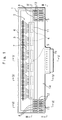
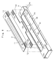
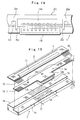
- Figs. 1-8 show a thermal printhead according to a first embodiment of the present invention.
- the thermal printhead includes a metallic heat sink plate 1 made of aluminum for example.
- the heat sink plate 1 has a stepped upper surface having a higher first supporting surface 1a and a lower second supporting surface 1b.
- the first supporting surface 1a carries a head substrate 2, whereas the second supporting surface 1b carries a printed circuit board 14.
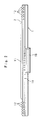
- the difference in height between the first supporting surface 1a and the second supporting surface 1b is designated by Reference H in Fig. 4.
- the head substrate 2 which has an elongated rectangular configuration, is made of an insulating material such as a ceramic.
- the head substrate 2 has an upper surface formed with a linear heating resistor 3 extending longitudinally thereof together with an array of plural drive ICs 4 arranged in parallel to the heating resistor 3.
- a thermistor 5 (see Figs. 1 and 5) as a temperature sensing device is provided between the two central drive ICs of the drive ICs 4.
- the upper surface of the head substrate 2 is also formed with a common electrode 6 and plural individual electrodes 7 both of which are electrically connected to the heating resistor 3.
- the upper surface of the head substrate 2 is formed with a wiring pattern WP (partially shown in Fig.
- connection terminals 8 are electrically connected to the above-mentioned wiring pattern WP.
- the both ends of the common electrode 6 as well as the connection terminals 8 serve as connection terminals for external electrical connection.
- each of the individual electrodes 7 is wire-bonded via a thin metal wire 9 to one of the drive ICs 4, whereas each of the drive ICs 4 is wire-bonded via a thin metal wire 10 to the wiring pattern WP.
- Each of the drive ICs 4, the thermistor 5, and each of the metal wires 9, 10 are covered with a protection coating 11 made of a synthetic resin (see Figs. 1, 2, 4, and 5).
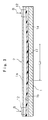
- One of the longitudinal edges of the head substrate 2 is arranged to project by a suitable amount E from the first supporting surface 1a of the heat sink plate 1 toward the second supporting surface 1b (see Figs. 4-7).
- the projecting amount E is so determined that the drive ICs 4 and the thermistor 5 project from the first supporting surface 1a toward the second supporting surface 1b.
- the head substrate 2 is attached generally at a longitudinally central portion of a length L1 to the first supporting surface 1a of the heat sink plate 1 by an adhesive 13 (an ultraviolet-setting adhesive for example).
- an adhesive 13 an ultraviolet-setting adhesive for example.
- the whole length of the head substrate 2 may be attached to the heat sink plate 1 by adhesive tape.
- each of the terminal leads 12 which is formed by punching a metal plate, has a clip portion 12a for clipping engagement with the head substrate 2 and a stem portion 12b extending obliquely from the clip portion 12a toward the second supporting surface 1b of the heat sink plate 1.
- the printed circuit board 14 on the second supporting surface 1b of the heat sink plate 1, which has an elongated rectangular configuration, is made of an insulating material such as a synthetic resin.
- the printed circuit board 14 has an upper surface formed with, adjacent the both shorter edges thereof, connection electrodes 15 corresponding to the connection terminals 8 on the head substrate 2.
- the upper surface of the printed circuit board 14 is also formed with a wiring pattern (not shown) for electrically connecting the connection electrodes 15 to a connector 16 for external connection which is provided at a generally central portion of the printed circuit board 14.
- To the connector 16 is electrically connected, for instance, a flexible cable (not shown) extending from a control unit (not shown).
- the printed circuit board 14 is attached generally at a longitudinally central portion of a length of L2 (which substantially corresponds to the attached portion L1 of the head substrate 2) to the second supporting surface 1b of the heat sink plate 1 by an adhesive 17 (an ultraviolet-setting adhesive for example). As shown in Figs. 4-7, in this attached state, the printed circuit board 14 extends into under the head substrate 2.
- one of the longitudinal edges of the printed circuit board 14 is located at the boundary between the first supporting surface 1a and second supporting surface 1b of the heat sink plate 1.
- an overlapping amount of the printed circuit board 14 and the head substrate 2 is equal to the projecting amount E of the projecting longitudinal edge of the head substrate 2. Since the thickness T of the printed circuit board 14 is smaller than the difference H in height between the first supporting surface 1a and second supporting surface 1b of the heat sink plate 1, there is provided a clearance 18 between the printed circuit board 14 and the head substrate 2.
- the stem portion 12b of each terminal lead 12 extends obliquely downward toward the second supporting surface 1b of the heat sink plate 2 (see Figs. 6 and 7).
- the stem portion 12b of the terminal lead 12 comes into contact with a corresponding connection electrode 15 on the printed circuit board 14.
- the terminal lead 12 is connected to the corresponding terminal electrode 15 by a solder 19.
- the tip of the stem portion 12b of the terminal lead is formed with a tapered surface inclining at a predetermined angle ⁇ relative to a vertical line perpendicular to the upper surface of the printed circuit board 14.
- the thermal printhead having the above-described structure has the following advantages.
- the head substrate 2 and the printed circuit board 14 overlap onto each other widthwise by a predetermined amount E.
- the thermal printhead including the heat sink plate 1 can be reduced in size, thereby promoting miniaturization.
- the clearance 18 in communication with the atmosphere is provided between the head substrate 2 and the printed circuit board 14, the exposed area of the head substrate 2 to the atmosphere and the exposed area of the heat sink plate 1 to the atmosphere can be made larger than if the printed circuit board 14 comes into direct contact with the head substrate 2 from below.
- heat-dissipating performance from the head substrate 2 can be improved to a great extent, thereby preventing the electronic elements (the drive ICs 4 in particular) from suffering damages due to overheating of the head substrate 2.
- the presence of the clearance 8 can surely prevent a thicknesswise thermal expansion of th e printed circuit board 14 from affecting the head substrate 2, thereby reducing the possibility of printing irregularities even for high-speed printing, which generates totally a larger amount of heat.
- one of the longitudinal edges of the head substrate 2 projects from the first supporting surface 1a of the heat sink plate 1, and the thermistor 5 is mounted on the projecting edge of the head substrate 2 (see Figs. 1 and 5).
- the projecting edge of the head substrate 2 releases less heat than the portion held in direct contact with the heat sink plate 1 (though more heat than if in direct contact with the printed circuit board 14). Therefore, by mounting the temperature sensing thermistor 5 on the projecting portion of the head substrate 2, response and accuracy to a rise in temperature can be surely improved than if the thermistor 5 is mounted on the head substrate 2 at a portion thereof which comes into direct contact with the heat sink plate 1.
- connection terminals 8 on the head substrate 2 are electrically connected to the connection electrodes 15 on the printed circuit board 14 via the clip-type terminal leads 12.
- the stem portion 12b of the terminal lead 12 is elastic, the deflection of the stem portion 12b of the terminal lead 12 can absorb the difference in longitudinal thermal expansion between the head substrate 2 and the printed circuit board 14.
- the printed circuit board 14 made of synthetic resin has a larger coefficient of thermal expansion than the head substrate 2 made of ceramic, the printed circuit board 14 longitudinally expands more than the head substrate 2 due to the heat generated during printing operation. Therefore, if there is no absorption of the difference in expansion by the deflection of the stem portion 12b of the terminal lead 12, both ends of the head substrate 2 are slightly raised above the heat sink plate 1, thereby reducing the amount of heat released to the heat sink plate 1.
- the stem portion 12b of each terminal lead 12 is arranged to extend obliquely downward toward the second supporting surface 1b of the heat sink plate 1 for coming into contact with a corresponding connection electrode 15 on the printed circuit board 14.
- the soldering strength can be further increased by causing a tip surface 12c of the terminal lead 12 to incline by a suitable angle ⁇ to enlarge the area in contact with the solder 19.
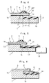
- Figs. 9-12 show a method of assembling the thermal printhead according to the first embodiment.
- an assemble jig A is prepared.
- the jig A has a first positioning portion A1 for setting the head substrate 2 at a higher position and a second positioning portion A2 for setting the printed circuit board 14 at a lower position.
- the difference H0 in height between the first positioning portion A1 and the second positioning portion A2 is set to be slightly smaller than the difference H in height between the first and second supporting surfaces 1a, 1b of the heat sink plate 1.
- the head substrate 2 is mounted on the first positioning portion A1 of the jig A, whereas the printed circuit board 14 is mounted on the second positioning portion A2.
- the head substrate 2 and the printed circuit board 14 are automatically set in positionally proper relation to each other, longitudinally and widthwise.
- the terminal leads 12 secured adjacent the both ends of the head substrate 2 are soldered to the respective connection electrodes 15 on the printed circuit board 14 (see Figs. 6 and 7).
- the stem portion 12b of each terminal lead 12 on the head substrate 2 is substantially in an original state.
- head substrate 2 and printed circuit board 14 are taken out from the jig A, and thereafter they are attached onto the heat sink plate 1, as shown in Fig. 12.
- the head substrate 2 is attached generally at the longitudinally central portion L1 to the first supporting surface 1a of the heat sink plate 1 by the adhesive 13
- the printed circuit board 14 is attached generally at the longitudinally central portion L2 to the second supporting surface 1b of the heat sink plate 1 by the adhesive 17.
- the printed circuit board 14 is deformed in a manner such that the both ends thereof are slightly raised above the second supporting surface 1b of the heat sink plate 1, or in a downwardly convex manner as a whole.
- the printed circuit board 14 is deformed in a downwardly convex manner so that the elastically resuming force of the printed circuit board 14 acts on the both ends of the head substrate 2 via each of the terminal leads 12.
- the both ends of the head substrate 2 are constantly pressed to the heat sink plate 1, thereby surely preventing the both ends of the head substrate 2 from slightly rising from the heat sink plate 1.
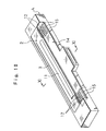
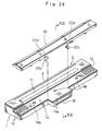
- Figs. 13-22 show a thermal printhead according to a second embodiment of the present invention.
- the thermal printhead of the second embodiment is basically similar to the thermal printhead of the first embodiment (see Figs. 1-12). Therefore, constituting elements common to the both embodiments are designated by the same reference numerals and a detailed description is not given.
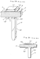
- the thermal printhead according to the second embodiment also includes an elongated cover member 20 for covering substantially the whole of the printed circuit board 14 and the projecting longitudinal edge of the head substrate 2.
- the cover member 20 is made of an electrostatically conductive material having a volume resistivity of 10 5 -10 9 ( ⁇ ⁇ cm), and has an antistatic property.
- Such an electrostatically conductive material can be made by mixing a synthetic resin such as epoxy resin with a suitable amount of conductive powder such as carbon powder.
- One longitudinal edge of the cover member 20 is integrally formed with a plurality of engagement tongues 20a.
- the lower surface of the cover member 20 is integrally formed with a plurality of abutment legs 20b adjacent to the above-mentioned one longitudinal edge.
- the other longitudinal edge of the lower surface of the cover member 20 is integrally formed with a pair of elastic engagement legs 20c with a longitudinal predetermined spacing therebetween.
- a groove 20d may be formed on the longitudinal outside of each engagement leg 20c, as shown in Figs. 18 and 20.
- each engagement tongue 20a of the cover member 20 comes into engagement with the projecting longitudinal edge of the head substrate 2 from below (that is, from the side of the clearance 18).
- the printed circuit board 14 is formed with a plurality of through holes 14b corresponding to the abutment legs 20b of the cover member 20 (see Figs. 14, 15, 19 and 20).
- the abutment legs 20b are held in direct contact with the second supporting surface 1b of the heat sink plate 1 via the through holes 14b of the printed circuit board 14.
- the printed circuit board 14 also includes a central projecting portion 14a which projects from the second supporting surface 1b of the heat sink plate 1. Both of the engagement legs 20c of the cover member 20 elastically engage the central projecting portion 14a (see Figs. 13, 14, 17, 18 and 20).
- the abutment legs 20b of the cover member 20 are closer to the engagement tongues 20a rather than to the engagement legs 20c.
- the cover member 20 can be easily and surely secured to the printed circuit board 14 and heat sink plate 1 by utilizing the principles of the lever and fulcrum, that is, in a manner such that firstly the engagement tongues 20a are held in engagement with the projecting longitudinal edge of the head substrate 2 with the cover member 20 slightly inclined, and then the cover member 20 is simply pushed down in the direction of an arrow B.
- a printing medium 22 (thermosensitive paper for example) supported by a platen 21 is guided by the cover member 20.
- the cover member 20 is capable of conducting static electricity. Therefore, whenever static electricity is generated upon supplying a printing medium 22, it is conducted to the metallic heat sink plate 1 via the abutment legs 20b of the cover member 20. As a result, the drive ICs 4 and others can be prevented from suffering damages due to the static electricity. Since the cover member 20 simply engages the head substrate 2 only by the engagement tongues 20a, the longitudinal thermal expansion of the cover member 20 hardly affects the head substrate 2.
- the engagement legs 20c of the cover member 20 are arranged to elastically engage (in snapping engagement with) the central projecting portion 14a of the printed circuit board 14.
- the engagement legs 20c of the cover member 20 may be arranged to engage such a projecting longitudinal edge of the printed circuit board 14.
- the cover member 20 may be formed with engagement legs for engaging the projecting ends of the printed circuit board 14 in addition to the engagement legs 20c for engaging the central projecting portion 14a (or the projecting longitudinal edge) of the printed circuit board 14.
- the engagement tongues 20a for the head substrate 2 may not be needed.
- the plurality of terminal leads 12 are separately arranged at the both ends of the head substrate 2 and printed circuit board 14.
- the terminal leads 12 may be arranged together generally at a longitudinally central portion of the head substrate 2 and printed circuit board 14.
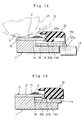
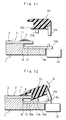
- Figs. 23-25 illustrate a preferred structure of each terminal lead 12 as well as a preferred structure of each connection terminal 8 on the head substrate 2.
- the upper surface of the head substrate 2 is formed with a glaze layer 2a upon which each connection terminal 8 is formed (in Figs. 1-22, the glaze layer 2a is not shown for convenience of illustration).
- the connection terminal 8 is formed to have a multi-layer structure (2-layer structure in the illustrated embodiment), including a gold layer 8a made by printing and sintering an organic gold paste and a silver layer 8b by printing and sintering a silver paste applied on the upper surface of the gold layer 8a.
- connection terminal 8 As a whole to have a large thickness by piling up the silver layer 8b.
- the gold layer 8a is formed by a single application of gold due to a problem of the cost, and therefore, the resulting thickness is very small, that is, about 0.7 ⁇ m. If the connection terminal 8 includes only the gold layer 8a, the thin gold layer 8a is scraped due to the friction caused when the the clip portion 12a of the terminal lead 12 is press-fitted, thereby bringing the clip portion 12a into direct contact with the glaze layer 2a of the head substrate 2, possibly resulting in incurring an improper state of electrical conduction with the connection terminal 8. However, when it is possible in terms of the cost to increase the thickness of the gold layer 8a, the silver layer 8b may be dispensed with.
- the piling up of the silver layer 8b also has the following advantage.
- the terminal lead 12 is produced by punching a metal plate of phosphor bronze into a suitable shape, subjecting the shaped metal to a bending process and, finally, plating it with solder or nickel to improve contact conduction property to the connection terminal 8. If the terminal lead 12 is solder-plated and comes into direct contact with the gold layer 8a, the solder melts due to the heat generated during the operation of the thermal printhead and is absorbed by the gold layer, thereby making it impossible to maintain a proper contact conduction between the terminal lead 12 and the connection terminal 8. Such a phenomenon is known as so-called "solder eating". The silver layer 8b piled up on the gold layer 8a serves to prevent or reduce the "solder eating".
- the terminal lead 12 has a clip portion 12a for engaging a longitudinal edge of the head substrate 2 and a stem portion 12b projecting from the clip portion 12a. More specifically, as the best shown in Fig. 25, the clip portion 12a of the terminal lead 12 includes a first engagement piece 121 for contacting with the connection terminal 8, a pair of second engagement pieces 122 for engaging the lower surface of the head substrate 2 and a connecting portion 123 for connecting the engagement pieces 121, 122 to one another. A clip opening 124 is present between the first engagement piece 121 and the second engagement pieces 122.
- the width of the clip opening 124 between the tip of the engagement piece 121 and the tips of the engagement pieces 122 is set to be larger than the thickness of the head substrate 2 including the glaze layer 2a, thereby facilitating the press-fitting of the clip portion 12a to the head substrate 2.
- the first engagement piece 121 includes in an intermediate part a convex contact portion 121a projecting toward the second engagement pieces 122.
- each of the second engagement pieces 122 includes a convex contact portion 122a projecting toward the first engagement piece 121.
- the width of the clip opening 124 between the first engagement 121 and the second engagement pieces 122 is set, at the positions of the convex contact portions 121a, 122a, to be smaller than the thickness of the head substrate 2 including the glaze layer 2a.
- the elastic resuming force of the engagement pieces 121, 122 permit the clip portion 12a to hold onto the head substrate 2.
- each of the convex contact portions 121a, 122a has a smooth structure, the mounting of the clip portion 12a onto the head substrate 2 can be performed smoothly.
- both of the side edges of the first engagement piece 121 of the clip portion 12a are formed with chamfers 125 facing the connection terminal 8.
- Each chamfer 125 extends continuously from the tip of the first engagement piece 121 at least to a point beyond the convex contact portion 121a.
- Each chamfer 125 may be an inclined surface as shown in Fig. 24 or a curved surface.
- the dimension of the chamfer 125 when viewed thicknesswise of the first engagement piece 121 is preferably no less than 0.05 mm for example. Such a dimension setting is not influenced by the thickness of the first engagement piece 121 (0.25 mm in the illustrated embodiment).
- the chamfers 125 may be formed by partially filing down the respective side edges of the first engagement pieces 121, it may be also formed by plastically deforming the same side edges in the direction away from the second engagement pieces 122.
- the contact condition between the first engagement piece 121" and the connection terminal 8'' becomes worse. If the first engagement piece 121" and the connection terminal 8'' are electrically connected by separate soldering, the inferior contact condition therebetween is hardly a problem. In such a case, however, a sufficient spacing (more than 1.5 mm for example) should be provided between the connection terminals for preventing the adjacent connection terminals from being short-circuited, thereby making it impossible to dispose a large number of connection terminals in a region of limited dimensions.
- the first engagement piece 121 when both of the side edges of the first engagement piece 121 are provided with chamfers 125 as shown in Figs. 23-25, the first engagement piece 121 partially scrapes the silver layer 8b of the connection terminal 8 between the both chamfers 125, thereby establishing a surface contact.
- the chamfers 125 partially contact with the connection terminal 8 due to the scraping into the silver layer 8b. Therefore, without performing separate soldering, the clip portion 12a of the terminal lead 12 and the connection terminal 8 can be held in a proper contact condition (electrically conductive condition) to each other.
- connection portion between the first engagement piece 121 of the clip portion 12a and the connection terminal 8 is enclosed by a transparent insulating resin 21.
- the insulating resin 21 serves to reinforce the connection between the clip portion 12a and the connection terminal 8, while preventing the drive ICs from breaking down due to the passage of the static electricity, which is generated during printing operation of the thermal printhead, through the connection terminals 8.
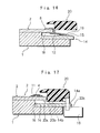
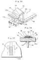
- Figs. 26 and 27 illustrate another preferred structure of the terminal lead together with another preferred structure of each connection terminal on the head substrate 2.
- connection terminal 8' shown in Fig. 26 has a multi-layer structure (3-layer structure in the illustrated embodiment), including a gold layer 8a', a silver layer 8b' formed on the upper surface of the gold layer 8a' and a silver-palladium (Ag-Pd) layer 8c' formed on the upper surface of the silver layer 8b'.
- the silver-palladium layer 8c' is provided for more certain prevention of the "solder eating" when the terminal lead 12' is solder-plated. However, as already described, even the silver layer 8b' alone can prevent the "solder eating" to some extent.
- the terminal lead 12' has a clip portion 12a' engaging a longitudinal edge of the head substrate 2 and a stem portion 12b' projecting from the clip portion 12a'.
- the clip portion 12a' has a first engagement piece 121' in contact with the connection terminal 8', a pair of second engagement pieces 122' engaging the lower surface of the head substrate 2 and a connection portion (not shown) for connecting the engagement pieces 121', 122' to one another.
- the first engagement piece 121' has a contact portion 121a' for the connection terminal 8' wherein the contact portion as a whole is convexly curved in transverse section thereof. As a result, both side edges 125' of the first engagement piece 121' are offset away from the connection terminal 8'.
- the first engagement piece 121" is not formed in parallel to the second engagement pieces 122" when viewed transversely.
- the first engagement piece 121" is thus inclined, only one of the side edges is held in contact with the connection terminal 8", thereby failing to realize a proper electrical contact between the clip portion 12a" and the connection terminal 8". This problem becomes outstanding especially when burrs (the elements C in Fig. 28) are formed on the clip portion 12a".
- the contact portion 121a' of the first engagement piece 121' as a whole has a convexly curved section when viewed transversely. Therefore, even when the first engagement piece 121' is transversely inclined relative to the second engagement pieces 122', the first engagement piece is similarly held in contact with the connection terminal 8' and scrapes the connection terminal 8' (the exposed silver-palladium layer 8c') in a region 22 of a generally constant width as shown in Fig. 27 when the clip portion 12a' is press-fitted onto the head substrate 2'. As a result, a proper electrical connection can be obtained between the clip portion 12a' and the connection terminal 8', thereby dispensing with separate soldering.
- the drive ICs 4 may be mounted on the printed circuit board 14 instead of on the head substrate 2.
Claims (16)
- Thermodruckkopf umfassend:dadurch gekennzeichnet,eine abgestufte Wärmesenke-Platte (Kühlkörper 1) mit einer oberen ersten Stützfläche (tragende Oberfläche 1a) und einer unteren zweiten Stützfläche (tragende Oberfläche 1b);ein auf der ersten tragenden Oberfläche (1a) des Kühlkörpers (1) aufgebrachtes und mit Druckpunkten (3) versehenes Kopfsubstrat (2); undeine auf der zweiten tragenden Oberfläche (1b) des Kühlkörpers (1) aufgebrachte und mit einem Verdrahtungsmuster ausgebildete gedruckte Leiterplatine (14);wobei das Kopfsubstrat (2) eine von der ersten tragenden Oberfläche (1a) des Kühlkörpers (1) in Richtung der zweiten tragenden Oberfläche (1b) hervorstehende Kante aufweist;wobei die erste tragende Oberfläche (1a) und die zweite tragende Oberfläche (1b) in eine gemeinsame Richtung zeigen;
daß die gedruckte Leiterplatine (14) die hervorstehende Kante des Kopfsubstrates (2) mit einem dazwischen liegenden vorbestimmten Abstand (18) überlappt. - Thermodruckkopf nach Anspruch 1, in dem die hervorstehende Kante des Kopfsubstrates (2) mit einem temperaturfühlenden Termistor (5) versehen ist.
- Thermodruckkopf nach Anspruch 1, wobei das Kopfsubstrat (2) mit einer Mehrzahl von Treiber-IC's (4) zum Treiben der Druckpunkte (3) versehen ist, die hervorstehende Kante des Kopfsubstrates (2) mit einer Mehrzahl von elektrisch mit den Treiber-IC's (4) verbundenen Verbindungsanschlüssen (8) ausgebildet ist, die gedruckte Leiterplatine (14) mit einer Mehrzahl von, den Verbindungsanschlüssen (8) auf dem Kopfsubstrat (2) entsprechenden Verbindungselektroden (15) versehen ist, jeder der Verbindungsanschlüsse (8) auf dem Kopfsubstrat (2) elektrisch mit einer entsprechenden Verbindungselektrode (15) auf der gedruckten Leiterplatine (14) mittels einer metallischen klammerartigen Klemmenzuleitung (12) verbunden ist, die Klemmenzuleitung (12) einen Klammerabschnitt (12a) aufweist, welcher in umklammernder Verbindung mit der hervorstehenden Kante des Kopfsubstrates (2) gehalten wird und einen Stammabschnitt (12b) aufweist, welcher sich von dem Klammerabschnitt (12a) in Richtung der gedruckten Leiterplatine (14) erstreckt.
- Thermodruckkopf nach Anspruch 3, wobei der Stammabschnitt (12b) der Klemmenzuleitung (12) sich zum Anlöten an die entsprechende Verbindungselektrode (15) schräg in Richtung der gedruckten Leiterplatine (14) erstreckt.
- Thermodruckkopf nach Anspruch 3, in dem der Stammabschnitt (12b) der Klemmenzuleitung (12) eine Punktoberfläche (12c) aufweist, welche sich relativ zu der gedruckten Leiterplatine (14) in einem stumpfen Winkel abwärts neigt.
- Thermodruckkopf nach Anspruch 3, wobei der Klammerabschnitt (12a) der Klemmenzuleitung ein im Kontakt mit dem entsprechenden Verbindungsanschluß (8) auf dem Kopfsubstrat (2) gehaltenes Kuppelstück aufweist, dessen beide Seitenkanten weg von dem Verbindungsanschluß (8) abgeknickt sind.
- Thermodruckkopf nach Anspruch 6, wobei beide Seitenkanten des Verbindungsstückes der Klemmenzuleitung (12) abgeschrägt sind.
- Thermodruckkopf nach Anspruch 6, wobei das Verbindungsstück der Klemmenzuleitung (12) für den entsprechenden Verbindungsanschluß (8) einen Kontaktabschnitt aufweist, der als Ganzes im Querschnitt in Richtung des entsprechenden Verbindungsanschlusses (8) konvex gekrümmt ist.
- Thermodruckkopf nach Anspruch 3, wobei jeder Verbindungsanschluß (8) auf dem Kopfsubstrat (2) eine vielschichtige Struktur besitzt.
- Thermodruckkopf nach Anspruch 9, wobei jeder Verbindungsanschluß (8) des Kopfsubstrates (2) eine untere Schicht aus Gold und eine Oberflächenschicht entweder aus Silber oder Silber-Palladium umfaßt.
- Thermodruckkopf nach Anspruch 6, wobei das Verbindungsstück des Klammerabschnitts (12a) der Klemmenzuleitung (12) zusammen mit dem entsprechenden Verbindungsanschluß (8) auf dem Kopfsubstrat (2) von einem isolierenden Harz (11) eingeschlossen ist.
- Thermodruckkopf nach Anspruch 1, wobei das Kopfsubstrat (2) im allgemeinen an einem in Längsrichtung mittigen Abschnitt mit der ersten tragenden Oberfläche (1a) des Kühlkörpers (1) befestigt ist, die gedruckte Leiterplatine (14) im allgemeinen an einem in Längsrichtung mittigen Abschnitt mit der zweiten tragenden Oberfläche (1b) des Kühlkörpers (1) befestigt ist, beide Enden des Kopfsubstrats (2) mit beiden Enden der gedruckten Leiterplatine (14) entsprechend über eine Vielzahl von klammerartigen Klemmenzuleitungen (12) verbunden sind, die gedruckte Leiterplatine (14) so verformt ist, daß seine beiden Enden dem Kopfsubstrat (2) näher sind.
- Thermodruckkopf nach Anspruch 1, wobei die gedruckte Leiterplatine (14) mit einem in Richtung des Kopfsubstrates (2) hervorspringend Abdeckungsbauteil (20) bedeckt ist, da Abdeckungsbauteil (20) eine Mehrzahl von Verbindungsbeinen (20c) umfaßt, welche in einschnappender Verbindung mit vorherbestimmten Abschnitten der gedruckten Leiterplatine (14) gehalten werden, und wenigstens ein Stützbein (20b) umfaßt, welches auf dem Kühlkörper (1) ruht.
- Thermodruckkopf nach Anspruch 13, wobei das Abdeckungsbauteil (20) ferner wenigstens eine Verbindungszunge (20a) umfaßt, welche mit der hervorstehenden Kante des Kopfsubstrates (2) kuppelt.
- Thermodruckkopf nach Anspruch 14, wobei das Stützbein des Abdeckungsbauteils (20) zwischen jedem Verbindungsbein (20c) und der Verbindungszunge (20a), sowie an einer Position näher zu der Verbindungszunge (20a) angeordnet ist, wenn es der Breite des Abdeckungsbauteils (20) nach erblickt wird.
- Thermodruckkopf nach Anspruch 13, wobei das Abdeckungsbauteil (20) aus einem elektrostatisch leitenden Harz hergestellt ist.
Priority Applications (2)
| Application Number | Priority Date | Filing Date | Title |
|---|---|---|---|
| EP99121813A EP0978384B1 (de) | 1994-10-03 | 1995-10-03 | Thermodruckkopf |
| EP99121818A EP0978385B1 (de) | 1994-10-03 | 1995-10-03 | Elektrische Verbindungsstruktur |
Applications Claiming Priority (16)
| Application Number | Priority Date | Filing Date | Title |
|---|---|---|---|
| JP23894694 | 1994-10-03 | ||
| JP238946/94 | 1994-10-03 | ||
| JP6238946A JP2774941B2 (ja) | 1994-10-03 | 1994-10-03 | サーマルプリントヘッドの組立て方法 |
| JP24098594 | 1994-10-05 | ||
| JP240985/94 | 1994-10-05 | ||
| JP24098594 | 1994-10-05 | ||
| JP327320/94 | 1994-12-28 | ||
| JP32732094 | 1994-12-28 | ||
| JP32732094 | 1994-12-28 | ||
| JP1000095 | 1995-01-25 | ||
| JP10000/95 | 1995-01-25 | ||
| JP1000095 | 1995-01-25 | ||
| JP62541/95 | 1995-03-22 | ||
| JP6254195A JP3248828B2 (ja) | 1995-03-22 | 1995-03-22 | サーマルプリントヘッドの構造 |
| JP6254195 | 1995-03-22 | ||
| PCT/JP1995/002015 WO1996010490A1 (en) | 1994-10-03 | 1995-10-03 | Thermal printing head, and clip type terminal lead and cover used for the same |
Related Child Applications (2)
| Application Number | Title | Priority Date | Filing Date |
|---|---|---|---|
| EP99121813A Division EP0978384B1 (de) | 1994-10-03 | 1995-10-03 | Thermodruckkopf |
| EP99121818A Division EP0978385B1 (de) | 1994-10-03 | 1995-10-03 | Elektrische Verbindungsstruktur |
Publications (3)
| Publication Number | Publication Date |
|---|---|
| EP0729839A1 EP0729839A1 (de) | 1996-09-04 |
| EP0729839A4 EP0729839A4 (de) | 1997-01-08 |
| EP0729839B1 true EP0729839B1 (de) | 2000-05-17 |
Family
ID=27519133
Family Applications (3)
| Application Number | Title | Priority Date | Filing Date |
|---|---|---|---|
| EP95932962A Expired - Lifetime EP0729839B1 (de) | 1994-10-03 | 1995-10-03 | Thermodruckkopf |
| EP99121818A Expired - Lifetime EP0978385B1 (de) | 1994-10-03 | 1995-10-03 | Elektrische Verbindungsstruktur |
| EP99121813A Expired - Lifetime EP0978384B1 (de) | 1994-10-03 | 1995-10-03 | Thermodruckkopf |
Family Applications After (2)
| Application Number | Title | Priority Date | Filing Date |
|---|---|---|---|
| EP99121818A Expired - Lifetime EP0978385B1 (de) | 1994-10-03 | 1995-10-03 | Elektrische Verbindungsstruktur |
| EP99121813A Expired - Lifetime EP0978384B1 (de) | 1994-10-03 | 1995-10-03 | Thermodruckkopf |
Country Status (7)
| Country | Link |
|---|---|
| US (1) | US5739837A (de) |
| EP (3) | EP0729839B1 (de) |
| KR (1) | KR0173430B1 (de) |
| CN (3) | CN1056339C (de) |
| DE (3) | DE69525867T2 (de) |
| TW (1) | TW285714B (de) |
| WO (1) | WO1996010490A1 (de) |
Families Citing this family (23)
| Publication number | Priority date | Publication date | Assignee | Title |
|---|---|---|---|---|
| JP3469380B2 (ja) * | 1995-12-08 | 2003-11-25 | ローム株式会社 | サーマルプリントヘッドおよびその製造方法 |
| JP3238893B2 (ja) * | 1998-01-30 | 2001-12-17 | ローム株式会社 | サーマルプリントヘッドにおけるカバー装置 |
| JP4428472B2 (ja) * | 1998-12-10 | 2010-03-10 | ローム株式会社 | クリップコネクタの取付け構造、クリップコネクタの取付け方法、およびクリップコネクタ |
| JP3825199B2 (ja) * | 1999-04-13 | 2006-09-20 | ローム株式会社 | サーマルプリントヘッドにおけるカバー装置 |
| JP4323022B2 (ja) | 1999-09-21 | 2009-09-02 | ローム株式会社 | サーマルプリントヘッドの製造方法 |
| JP2001105645A (ja) * | 1999-10-13 | 2001-04-17 | Rohm Co Ltd | サーマルプリントヘッドおよびクリップピン |
| SE0101689L (sv) * | 2001-05-15 | 2002-10-01 | Safetrack Baavhammar Ab | Förbindningsstycke av elektriskt ledande material, företrädesvis en kabelsko samt sätt för dess framställning |
| FR2837424B1 (fr) * | 2002-03-21 | 2004-09-10 | A P S Engineering | Tete d'impression thermique dont l'organe de guidage de la bande a imprimer est agence pour permettre une mise a la masse de la tete d'impression |
| US7625072B2 (en) * | 2004-07-22 | 2009-12-01 | Canon Kabushiki Kaisha | Ink jet recording head and recording apparatus |
| CN100411875C (zh) * | 2005-04-15 | 2008-08-20 | 光宝科技股份有限公司 | 具有温度控制功能的热打印机打印头 |
| KR100601725B1 (ko) * | 2005-06-10 | 2006-07-18 | 삼성전자주식회사 | 감열방식 화상형성장치 |
| JP5200360B2 (ja) | 2006-09-29 | 2013-06-05 | 富士ゼロックス株式会社 | 露光装置および画像形成装置 |
| US20090241116A1 (en) * | 2008-03-21 | 2009-09-24 | Dell Products L.P. | Systems and Methods for Automating Tasks Associated with an Application Packaging Job |
| US20090240548A1 (en) * | 2008-03-21 | 2009-09-24 | Dell Products L.P. | Systems and Methods for Generating a Configurable Workflow for Application Packaging Jobs |
| US20090240634A1 (en) * | 2008-03-21 | 2009-09-24 | Dell Products L. P. | Systems and Methods for Automating Calculation of Costs Associated with an Application Packaging Job |
| KR101338116B1 (ko) | 2009-07-09 | 2013-12-06 | 엘지디스플레이 주식회사 | 액정표시장치 |
| EP2558300B1 (de) * | 2010-04-12 | 2016-11-02 | ZIH Corp. | Druckermobilität und skalierbarkeit |
| CN102529416B (zh) * | 2010-11-30 | 2016-01-20 | 罗姆股份有限公司 | 热敏打印头 |
| CN102490475B (zh) * | 2011-11-30 | 2014-06-25 | 山东华菱电子有限公司 | 热敏打印头 |
| WO2013129020A1 (ja) * | 2012-02-28 | 2013-09-06 | 京セラ株式会社 | サーマルヘッドおよびこれを備えるサーマルプリンタ |
| JP5739919B2 (ja) * | 2013-01-10 | 2015-06-24 | 東芝テック株式会社 | サーマルプリンタ装置 |
| JP2017183686A (ja) * | 2016-03-29 | 2017-10-05 | 日本碍子株式会社 | 金属配線接合構造及びその製法 |
| WO2021200669A1 (ja) * | 2020-03-31 | 2021-10-07 | 京セラ株式会社 | サーマルヘッドおよびサーマルプリンタ |
Family Cites Families (27)
| Publication number | Priority date | Publication date | Assignee | Title |
|---|---|---|---|---|
| JPS528513A (en) * | 1975-07-10 | 1977-01-22 | Sekisui Koji Kk | Structural unit board for tank construction |
| JPS5587581A (en) * | 1978-12-27 | 1980-07-02 | Canon Inc | Thermal printer |
| JPS56109068A (en) * | 1980-02-04 | 1981-08-29 | Nippon Telegr & Teleph Corp <Ntt> | Recorder for multitone |
| JPS57121543U (de) * | 1981-01-23 | 1982-07-28 | ||
| JPS61132356A (ja) * | 1984-12-03 | 1986-06-19 | Hitachi Ltd | 感熱記録ヘツド |
| JPH0354920Y2 (de) * | 1985-06-04 | 1991-12-05 | ||
| JPS62170359A (ja) * | 1986-01-23 | 1987-07-27 | Nec Corp | サ−マルヘツド |
| BR8701399A (pt) * | 1986-04-03 | 1988-01-05 | Du Pont | Tira de contacto e processo para a producao de uma fileira de conectores de grampo de borda,ou de um unico conector de grampo de borda |
| JPS63179764A (ja) * | 1987-01-22 | 1988-07-23 | Konica Corp | 感熱記録ヘツド |
| JP2629007B2 (ja) * | 1987-09-21 | 1997-07-09 | 京セラ株式会社 | サーマルヘッド |
| JPH0765355B2 (ja) * | 1987-11-13 | 1995-07-19 | ナショナル住宅産業株式会社 | 外壁パネル |
| JPH01127749U (de) * | 1988-02-19 | 1989-08-31 | ||
| JP2531463Y2 (ja) * | 1989-01-10 | 1997-04-02 | ローム株式会社 | サーマルヘッド |
| JP2793230B2 (ja) * | 1989-03-01 | 1998-09-03 | 京セラ株式会社 | サーマルヘッド |
| JPH02286261A (ja) * | 1989-04-27 | 1990-11-26 | Rohm Co Ltd | サーマルヘッド |
| JPH02292055A (ja) * | 1989-05-02 | 1990-12-03 | Rohm Co Ltd | サーマルヘッド |
| JPH0635382Y2 (ja) * | 1989-05-19 | 1994-09-14 | 富士電機株式会社 | 混成集積回路のリード端子取付構造 |
| JPH0357656A (ja) * | 1989-07-26 | 1991-03-13 | Nec Corp | サーマルヘッド |
| JPH0438670U (de) * | 1990-07-31 | 1992-03-31 | ||
| JP2538778Y2 (ja) * | 1990-08-31 | 1997-06-18 | 京セラ株式会社 | 画像形成装置 |
| JPH04191057A (ja) * | 1990-11-27 | 1992-07-09 | Seiko Instr Inc | サーマルヘッド |
| JP3228974B2 (ja) * | 1990-12-19 | 2001-11-12 | ローム株式会社 | ライン型サーマルプリントヘッド |
| EP0501707B1 (de) * | 1991-02-26 | 1996-07-03 | Rohm Co., Ltd. | Steuervorrichtung für Thermo-Druckkopf |
| JPH04282262A (ja) * | 1991-03-11 | 1992-10-07 | Mitsubishi Electric Corp | サーマルヘッド |
| JP3101394B2 (ja) * | 1992-01-31 | 2000-10-23 | ローム株式会社 | プリンタユニット及びそれを備えるサーマルヘッド |
| US5335002A (en) * | 1991-09-30 | 1994-08-02 | Rohm Co., Ltd. | Printing head and printer incorporating the same |
| JP3297708B2 (ja) * | 1993-03-12 | 2002-07-02 | ローム株式会社 | コネクタ |
-
1995
- 1995-10-03 KR KR1019960702823A patent/KR0173430B1/ko not_active IP Right Cessation
- 1995-10-03 CN CN95190984A patent/CN1056339C/zh not_active Expired - Fee Related
- 1995-10-03 US US08/646,276 patent/US5739837A/en not_active Expired - Lifetime
- 1995-10-03 EP EP95932962A patent/EP0729839B1/de not_active Expired - Lifetime
- 1995-10-03 DE DE69525867T patent/DE69525867T2/de not_active Expired - Fee Related
- 1995-10-03 EP EP99121818A patent/EP0978385B1/de not_active Expired - Lifetime
- 1995-10-03 EP EP99121813A patent/EP0978384B1/de not_active Expired - Lifetime
- 1995-10-03 TW TW084110292A patent/TW285714B/zh active
- 1995-10-03 DE DE69525868T patent/DE69525868T2/de not_active Expired - Fee Related
- 1995-10-03 CN CNB991207467A patent/CN1157298C/zh not_active Expired - Fee Related
- 1995-10-03 WO PCT/JP1995/002015 patent/WO1996010490A1/ja active IP Right Grant
- 1995-10-03 DE DE69517002T patent/DE69517002T2/de not_active Expired - Fee Related
-
1999
- 1999-09-22 CN CN99120745A patent/CN1106945C/zh not_active Expired - Fee Related
Also Published As
| Publication number | Publication date |
|---|---|
| DE69517002T2 (de) | 2001-01-11 |
| DE69525867T2 (de) | 2002-11-21 |
| DE69517002D1 (de) | 2000-06-21 |
| TW285714B (de) | 1996-09-11 |
| CN1136294A (zh) | 1996-11-20 |
| CN1249994A (zh) | 2000-04-12 |
| CN1261584A (zh) | 2000-08-02 |
| EP0978385A3 (de) | 2000-03-15 |
| EP0729839A4 (de) | 1997-01-08 |
| EP0978384A3 (de) | 2000-05-10 |
| EP0729839A1 (de) | 1996-09-04 |
| DE69525867D1 (de) | 2002-04-18 |
| WO1996010490A1 (en) | 1996-04-11 |
| CN1056339C (zh) | 2000-09-13 |
| DE69525868T2 (de) | 2002-11-21 |
| DE69525868D1 (de) | 2002-04-18 |
| CN1157298C (zh) | 2004-07-14 |
| EP0978384A2 (de) | 2000-02-09 |
| US5739837A (en) | 1998-04-14 |
| EP0978385B1 (de) | 2002-03-13 |
| KR960706404A (ko) | 1996-12-09 |
| EP0978384B1 (de) | 2002-03-13 |
| KR0173430B1 (ko) | 1999-04-01 |
| EP0978385A2 (de) | 2000-02-09 |
| CN1106945C (zh) | 2003-04-30 |
Similar Documents
| Publication | Publication Date | Title |
|---|---|---|
| EP0729839B1 (de) | Thermodruckkopf | |
| US6727798B2 (en) | Flip chip resistor and its manufacturing method | |
| US7772961B2 (en) | Chip-shaped electronic part | |
| EP0535557B1 (de) | Druckkopf und Drucker, welcher diesen aufweist | |
| KR20010074468A (ko) | 열 싱크에 집적 회로 패키지의 와이어 본드 부착 | |
| US7616223B2 (en) | Thermal printhead | |
| KR100592137B1 (ko) | 전자부품의 실장방법 및 그 방법에 의해 제조된 전자회로장치 | |
| US7755467B2 (en) | Chip resistor | |
| CN110356122B (zh) | 热敏打印头 | |
| EP0711669A1 (de) | Thermischer druckkopf | |
| KR100381630B1 (ko) | 서멀 프린트 헤드 | |
| JP3526353B2 (ja) | 電子部品およびこれを備えたプリンタ | |
| US6606109B1 (en) | Thermal head and thermal head unit | |
| CN113924213A (zh) | 热敏打印头 | |
| US5495223A (en) | Hybrid integrated circuit device | |
| JP3248828B2 (ja) | サーマルプリントヘッドの構造 | |
| CN111038111B (zh) | 热敏打印头及其制造方法 | |
| JP3017158B2 (ja) | サーマルプリントヘッドの構造 | |
| JP3017157B2 (ja) | サーマルプリントヘッドの構造 | |
| CA2226957C (en) | Head device including drive ics enclosed by protective coating and method of forming the protective coating | |
| JP3353037B2 (ja) | チップ抵抗器 | |
| JPH08104017A (ja) | サーマルプリントヘッドの構造及びその組立て方法 | |
| KR20050070094A (ko) | 서멀 프린트 헤드 | |
| JP3170205B2 (ja) | サーマルヘッド |
Legal Events
| Date | Code | Title | Description |
|---|---|---|---|
| PUAI | Public reference made under article 153(3) epc to a published international application that has entered the european phase |
Free format text: ORIGINAL CODE: 0009012 |
|
| 17P | Request for examination filed |
Effective date: 19960511 |
|
| AK | Designated contracting states |
Kind code of ref document: A1 Designated state(s): DE FR GB IT |
|
| A4 | Supplementary search report drawn up and despatched | ||
| AK | Designated contracting states |
Kind code of ref document: A4 Designated state(s): DE FR GB IT |
|
| 17Q | First examination report despatched |
Effective date: 19980730 |
|
| GRAG | Despatch of communication of intention to grant |
Free format text: ORIGINAL CODE: EPIDOS AGRA |
|
| RTI1 | Title (correction) |
Free format text: THERMAL PRINTING HEAD |
|
| GRAG | Despatch of communication of intention to grant |
Free format text: ORIGINAL CODE: EPIDOS AGRA |
|
| GRAH | Despatch of communication of intention to grant a patent |
Free format text: ORIGINAL CODE: EPIDOS IGRA |
|
| GRAH | Despatch of communication of intention to grant a patent |
Free format text: ORIGINAL CODE: EPIDOS IGRA |
|
| GRAH | Despatch of communication of intention to grant a patent |
Free format text: ORIGINAL CODE: EPIDOS IGRA |
|
| GRAA | (expected) grant |
Free format text: ORIGINAL CODE: 0009210 |
|
| AK | Designated contracting states |
Kind code of ref document: B1 Designated state(s): DE FR GB IT |
|
| RIC1 | Information provided on ipc code assigned before grant |
Free format text: 7B 41J 2/335 A, 7H 01R 12/16 B |
|
| ITF | It: translation for a ep patent filed |
Owner name: FIAMMENGHI - DOMENIGHETTI |
|
| REF | Corresponds to: |
Ref document number: 69517002 Country of ref document: DE Date of ref document: 20000621 |
|
| ET | Fr: translation filed | ||
| PLBE | No opposition filed within time limit |
Free format text: ORIGINAL CODE: 0009261 |
|
| STAA | Information on the status of an ep patent application or granted ep patent |
Free format text: STATUS: NO OPPOSITION FILED WITHIN TIME LIMIT |
|
| 26N | No opposition filed | ||
| REG | Reference to a national code |
Ref country code: GB Ref legal event code: IF02 |
|
| PGFP | Annual fee paid to national office [announced via postgrant information from national office to epo] |
Ref country code: DE Payment date: 20081014 Year of fee payment: 14 |
|
| PGFP | Annual fee paid to national office [announced via postgrant information from national office to epo] |
Ref country code: IT Payment date: 20081028 Year of fee payment: 14 |
|
| PGFP | Annual fee paid to national office [announced via postgrant information from national office to epo] |
Ref country code: FR Payment date: 20081014 Year of fee payment: 14 |
|
| PGFP | Annual fee paid to national office [announced via postgrant information from national office to epo] |
Ref country code: GB Payment date: 20081001 Year of fee payment: 14 |
|
| REG | Reference to a national code |
Ref country code: FR Ref legal event code: ST Effective date: 20100630 |
|
| PG25 | Lapsed in a contracting state [announced via postgrant information from national office to epo] |
Ref country code: FR Free format text: LAPSE BECAUSE OF NON-PAYMENT OF DUE FEES Effective date: 20091102 Ref country code: DE Free format text: LAPSE BECAUSE OF NON-PAYMENT OF DUE FEES Effective date: 20100501 |
|
| PG25 | Lapsed in a contracting state [announced via postgrant information from national office to epo] |
Ref country code: GB Free format text: LAPSE BECAUSE OF NON-PAYMENT OF DUE FEES Effective date: 20091003 |
|
| PG25 | Lapsed in a contracting state [announced via postgrant information from national office to epo] |
Ref country code: IT Free format text: LAPSE BECAUSE OF NON-PAYMENT OF DUE FEES Effective date: 20091003 |