EP0726394B1 - A power supply for vibrating compressors - Google Patents
A power supply for vibrating compressors Download PDFInfo
- Publication number
- EP0726394B1 EP0726394B1 EP96101622A EP96101622A EP0726394B1 EP 0726394 B1 EP0726394 B1 EP 0726394B1 EP 96101622 A EP96101622 A EP 96101622A EP 96101622 A EP96101622 A EP 96101622A EP 0726394 B1 EP0726394 B1 EP 0726394B1
- Authority
- EP
- European Patent Office
- Prior art keywords
- voltage
- mosfet
- circuit
- output
- vibrating
- Prior art date
- Legal status (The legal status is an assumption and is not a legal conclusion. Google has not performed a legal analysis and makes no representation as to the accuracy of the status listed.)
- Expired - Lifetime
Links
Images


Classifications
-
- H—ELECTRICITY
- H02—GENERATION; CONVERSION OR DISTRIBUTION OF ELECTRIC POWER
- H02M—APPARATUS FOR CONVERSION BETWEEN AC AND AC, BETWEEN AC AND DC, OR BETWEEN DC AND DC, AND FOR USE WITH MAINS OR SIMILAR POWER SUPPLY SYSTEMS; CONVERSION OF DC OR AC INPUT POWER INTO SURGE OUTPUT POWER; CONTROL OR REGULATION THEREOF
- H02M7/00—Conversion of AC power input into DC power output; Conversion of DC power input into AC power output
- H02M7/42—Conversion of DC power input into AC power output without possibility of reversal
- H02M7/44—Conversion of DC power input into AC power output without possibility of reversal by static converters
- H02M7/48—Conversion of DC power input into AC power output without possibility of reversal by static converters using discharge tubes with control electrode or semiconductor devices with control electrode
- H02M7/53—Conversion of DC power input into AC power output without possibility of reversal by static converters using discharge tubes with control electrode or semiconductor devices with control electrode using devices of a triode or transistor type requiring continuous application of a control signal
- H02M7/537—Conversion of DC power input into AC power output without possibility of reversal by static converters using discharge tubes with control electrode or semiconductor devices with control electrode using devices of a triode or transistor type requiring continuous application of a control signal using semiconductor devices only, e.g. single switched pulse inverters
-
- F—MECHANICAL ENGINEERING; LIGHTING; HEATING; WEAPONS; BLASTING
- F04—POSITIVE - DISPLACEMENT MACHINES FOR LIQUIDS; PUMPS FOR LIQUIDS OR ELASTIC FLUIDS
- F04B—POSITIVE-DISPLACEMENT MACHINES FOR LIQUIDS; PUMPS
- F04B35/00—Piston pumps specially adapted for elastic fluids and characterised by the driving means to their working members, or by combination with, or adaptation to, specific driving engines or motors, not otherwise provided for
- F04B35/04—Piston pumps specially adapted for elastic fluids and characterised by the driving means to their working members, or by combination with, or adaptation to, specific driving engines or motors, not otherwise provided for the means being electric
- F04B35/045—Piston pumps specially adapted for elastic fluids and characterised by the driving means to their working members, or by combination with, or adaptation to, specific driving engines or motors, not otherwise provided for the means being electric using solenoids
Definitions
- This invention relates to a power supply for vibrating compressors, particularly to a power supply for vibrating compressors of a type having a vibrating drive coil in a magnetic field, in which a timing at which a counter electromotive force generated in the drive coil is returned near to 0 volts is detected, and an AC voltage is generated in synchronism with that timing to feed a drive current to the drive coil to ensure efficient operation of the vibrating compressor.
- Another type of power supply is also known, in which a battery voltage is boosted by a DC-DC converter using a transformer, and the boosted voltage is fed to the vibrating compressor.
- the switching element is a bipolar switching transistor whose base is grounded through another bipolar transistor and whose collector is directly connected to the compressor. Accordingly, the control circuit is complicated, since the base of the switching transistor is to be controlled through the other transistor whose base is controlled by the control circuit.
- the power supply of the invention comprises the features stated in claim 1.
- the MOSFET is connected in the source follower form, i.e. the source will directly be connected to the compressor, which connection corresponds to the emitter follower form of a bipolar transistor, whereas in the prior power supply the bipolar transistor is not connected as emitter follower.
- the MOSFET is simply controlled by applying its control voltage through the photocoupler, at the same time isolating the boosted (high) voltage side from the low voltage control side.
- the power supply for vibrating compressors of the invention supplies optimal voltage to the vibrating compressor by providing a DC voltage booster circuit portion in the preceding stage of the AC voltage generating circuit portion.
- the DC voltage of a commercially available battery can be boosted to a desired voltage, so that power of optimal voltage can be supplied to match different drive voltages required for specific vibrating compressors of different specifications, and the vibrating compressor can be operated efficiently with a fewer number of parts and a simplified circuit configuration.
- Fig. 1 shows a construction of a power supply for vibrating compressors according to this invention.
- Fig. 2 is a time chart of assistance in explaining the operation.
- Fig. 3 is a diagram of assistance in explaining the counter electromotive force generated in the vibrating compressor.
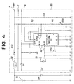
- Fig. 4 shows a construction of a voltage booster circuit portion of the power supply for vibrating compressors according to this invention.
- reference numeral 20 refers to an AC voltage generating circuit portion in which a vibrating compressor 1 is connected between the source of a n-channel MOSFET 2, which is a switching element, and the ground.
- the drain of the MOSFET 2 is connected to the positive +30-V side (Terminal e), for example, of the output of a voltage booster circuit portion 30 that will be described with reference to Fig. 4.
- the +30-V voltage can be obtained by boosting the +12-V output of a battery 3 in the voltage booster circuit portion 30.
- the vibrating compressor 1 is used for an automobile refrigerator, for example, and the battery 3 is of a commercially available automobile-mounted type.
- a driver 4 and a gate voltage circuit 5 are connected to the gate of the MOSFET 2, to which a gate voltage Vcc2 of approximately 12 V is fed from the gate-voltage circuit 5.
- the driver 4 and the gate-voltage circuit 5 are drive means for the switching element.
- the input of the gate-voltage circuit 5 is connected to the output (Terminal f) of the voltage booster circuit portion 30 shown in Fig. 4.
- the driver 4 receives a pulse signal (oscillation output) output by a timer IC 6 (NE555, for example), and generates a gate signal of the MOSFET 2 based on the received pulse signal.
- a source voltage Vcc1 is fed from a stabilization circuit 7 to the timer IC 6.
- the timer IC 6 as pulse generating means for switching the switching element operates as an astable multivibrator.
- the HIGH/LOW time of the output T Pin (or Terminal) No. 3 of the timer IC 6 is determined by resistors R3 and R4, and a capacitor C4 connected to Pins (or Terminals) Nos. 6 and 7 of the timer IC 6, as shown in the figure.
- the input of the stabilization circuit 7 is connected to the output (Terminal g) of the voltage booster circuit portion 30 shown in Fig. 4.
- Terminal g is also connected to a fan drive circuit 9 for driving a fan F, and used as the power supply thereof.
- the power supply shown in Fig. 1 (which will be described later) supplies to the vibrating compressor 1 the voltage obtained by boosting the voltage of the battery 3 in Fig. 4. Consequently, the power supply shown in Fig. 1 constitutes a single power supply, together with the voltage booster circuit portion 30 shown in Fig. 4.
- a timer forced operation circuit 8 which forcibly turns the HIGH-level output at Pin No. 3 to a LOW level at a predetermined timing.
- the signal output to Pin No. 3 is an output of the timer IC 6 and at the same time the output of the astable multivibrator that is the timer IC 6. Consequently, the timer IC 6 is an oscillation circuit, whose oscillation frequency is determined by external resistors R3 and R4 and an external capacitor C4, having the function to forcibly turn the HIGH level of the oscillation output thereof to a LOW level.
- the MOSFET 2 as a switching element provided according to this invention is driven by the driver 4.
- the driver 4 operates based on the oscillation output at Pin No. 3 of the timer IC 6.
- the drive output of the driver 4 is supplied by the gate-voltage circuit 5.
- the oscillation output of the timer IC 6 is forcibly changed by the timer forced operation circuit 8.
- the timer forced operation circuit 8 uses as an input the potential at a connecting point between the source of the MOSFET 2 and the vibrating compressor 1, and detects changes in the input. That is, the operation of the timer forced operation circuit 8 is dependent on (in synchronism with) the vibrating compressor 1.
- the switching of the MOSFET 2 is basically determined by the oscillation output of the timer IC 6, and can also be forcibly changed at a predetermined timing in synchronism with the operation of the vibrating compressor 1.
- the timing at which the switching operation is changed is a timing at which the counter electromotive force generated by the vibrating compressor 1 is recovered to the neighborhood of 0 volts, as will be described later.
- thermo-control circuit 10 for keeping the temperature in a refrigerator incorporating the vibrating compressor 1 constant.
- Numeral 11 refers to a counter electromotive force clamping circuit for clamping the counter electromotive force generated in the vibrating compressor 1.
- a source voltage Vcc2 which is approximately 12 V, for example, with respect to the source of the MOSFET, and stabilized by the gate-voltage circuit 5, is provided as a signal to be applied between the gate and source of the MOSFET 2. That is, when the MOSFET 2 is turned off, a counter electromotive force as shown in Fig. 3 is generated on the source side of the MOSFET 2 by the inductance of the vibrating compressor 1. This causes a diode D1 to conduct, charging a capacitor C3 to maintain the source voltage Vcc2. At this time, the source voltage Vcc2 and the source-drain voltage of the MOSFET 2 are kept at approximately 12 V by a constant-voltage diode ZD1.
- a phototransistor in a photocoupler IC (TLP521, for example) is turned on via a transistor TR3, which is usually turned off, and the source voltage Vcc2 of approximately 12 V is applied to the gate of the MOSFET 2 (Fig. 2 (2)), turning on the MOSFET 2.
- the boosted voltage of the battery 3 of Fig. 4 which will be described later, is applied to the vibrating compressor 1 (Fig. 2 (3)).
- the optimum time required for applying voltage to the vibrating compressor 1 is empirically determined in terms of the construction of the vibrating compressor 1, and set to the ON time T2. Note that the time T2 is a duration in which the MOSFET 2 is kept ON, while the time T1 is a duration in which the MOSFET 2 is kept OFF.
- the timer forced operation circuit 8 is therefore actuated at this timing, that is, the timing at which the counter electromotive force is about to exceed 0 volts, or recovered to the neighborhood of 0 volts (to substantially 0 volts). That is, the output (at Pin No. 3) of the timer IC 6 is forcibly reversed from H to L, that is, from OFF time T1 to ON time T2 at this timing. Consequently, the timer forced operation circuit 8 forcibly reverses the output of the pulse generating means (6) at the timing at which the counter electromotive force generated by the vibrating compressor 1 during the OFF period of the switching element (2) is recovered to the neighborhood of 0 volts. This allows voltage to be applied to the vibrating compressor 1 at the optimum timing, as will be described in the following.
- the base of the transistor TR2 in the timer forced operation circuit 8 is reverse-biased, turning off the transistor TR2.
- the transistor TR2 is turned on at that timing, causing potential of Point c on the collector side to reverse it from H to L (Fig. 2 (5)).
- the potential shift of Point c on the collector side from H to L is differentiated by a differentiation circuit consisting of a resistor R6 and a capacitor C6, and a sufficiently large trigger waveform as shown in Fig. 2 (6) appears at Point d on the cathode side of the diode D3.
- the aforementioned trigger waveform differentiated by the differentiation circuit consisting of the resistor R6 and the capacitor C6 is input to Pin No. 5 of the timer IC 6 via the diode D3.
- Pin No. 5 of the timer IC 6 serves as an input for controlling the ON time T1 output from Pin No. 3.
- the voltage at Pin No. 5 is therefore compared with the charging voltage of the capacitor C4 on Pin No. 6. If the voltage at Pin No. 5 is lower than that at Pin No. 6, control is effected so as to reverse the output at Pin No. 3.
- Pin No. 5 is usually set to the 2/3 of the source voltage Vcc1, and higher than the charging voltage of the capacitor C4 input to Pin No. 6 (Fig. 2 (7)). As shown in Fig. 2 (7), however, when a sufficiently large trigger waveform is input, the voltage at Pin No. 5 becomes lower than the charging voltage of the capacitor C4 at Pin No. 6 before the voltage at Pin No. 6 reaches the 2/3 of the source voltage Vcc1. That is, the timer IC 6, which is an astable multivibrator, is triggered, and the output at Pin No. 3 is caused to be forcibly reversed from H to L at that timing. That is, the HIGH-level time T1 at Pin No. 3 is forcibly terminated, shifting to the aforementioned ON time T2 (Fig. 2 (1)).
- an almost constant ON time T2 that is shorter than T2 0.693•R4•C4, as described above, can be obtained because the ON time T2 begins at a voltage lower than the 2/3 of Vcc1.
- the value of the ON time T2 in this invention is determined, taking into consideration the fact that the ON time T2 becomes shorter.
- the 1/3 of Vcc1 in Fig. 2 (7) represents the level at which the HIGH-level time is started on Pin No. 3 when the charging voltage of the capacitor C4 reaches this level in case that Pin No. 5 of the timer IC 6 is not used or not connected with the timer forced operation circuit 8.
- the 2/3 of Vcc1 represents the level at which the LOW-level time is started on Pin No. 3 when the charging voltage of the capacitor C4 reaches this level.
- the OP (operational) amplifier OP2 of the thermo-control circuit 10 compares at all times the voltage divided by a resistor R17 and a thermistor TH1 with a reference voltage obtained by dividing the stabilized Vcc1 voltage by resistors R18 and R20, and R19.
- the resistance value of the thermistor TH1 rises as temperature falls. Consequently, as the temperature in the refrigerator falls below a preset temperature, the output of the OP amplifier OP2 becomes L, cutting off the base current of the transistor TR3, turning off the transistor TR3. This causes the photodiode in the photocoupler IC to stop emitting light, continuously turning off the MOSFET 2. Consequently, voltage supply to the vibrating compressor 1 is stopped.
- the output of the OP amplifier OP2 is reversed to H.
- the output of the OP amplifier OP2 being H, the base current of the transistor TR3 is kept supplied, holding the transistor TR3 in the ON state, whereby the MOSFET 2 is caused to perform ON/OFF operation by a pulse signal output by the timer IC 6, causing the vibrating compressor 1 to resume operation.
- the output of the OP amplifier OP2 becomes L, as described above. With the output of the OP amplifier OP2 becoming L, however, both the transistors TR4 and TR5 of the fan drive circuit 9 are turned off, causing the fan F to stop. As the temperature in the refrigerator rises above the preset temperature, both the transistors TR4 and TR5 are turned ON, causing the fan F to operate. This leads to a power saving for the battery 3.
- Fig. 4 shows a construction of the voltage booster circuit portion 30 of the power supply for vibrating compressors according to this invention.
- the voltage booster circuit portion 30 is a transformerless circuit having voltage changing means for boosting the DC current of the battery 3 and changing the boosted voltage.
- the basic part of the voltage booster circuit portion 30 comprises a MOSFET 31, choke coil 32, diode D31, controlling switching IC (TL494, for example) 33, and capacitor C31.
- a PWM controlling signal having such a pulse width that the voltage (to be input to Pin No. 1) obtained by dividing the output voltage at Terminal e by a resistor R31, and a resistor R32 and a variable resistor VR31 becomes equal to the reference voltage at Pin No. 14 of the controlling switching IC 33 is output to Pin Nos. 9 and 10 of the controlling switching IC 33.
- This PWM controlling signal is impressed to the gate of the MOSFET 31 by the switching operation of the transistor TR31. With this, the MOSFET 31 is PWM-controlled.
- the voltage on the output side (Terminal e) is caused to change by changing the voltage obtained by dividing the output side (Terminal e) by the resistor R31, and the resistor R32 and the variable resistor VR31, that is by changing the pulse width of the PWM control signal output by Pin Nos. 9 and 10 of the controlling switching IC 33 by changing the variable resistor VR31, thereby changing the ON/OFF time ratio (on-duty) of the MOSFET 31.
- a DC voltage of 30 V for example, can be obtained on Terminal e in the voltage booster circuit portion 30 based on the DC voltage of 12 V of the commercially available battery 3 without using transformer.
- the DC voltage of the battery 3 is not limited to 12 V, but may be set to the voltage of an automobile battery, if the vibrating compressor is used on an automobile.
- the boosted voltage is also not limited to 30 V, but may be determined depending on the characteristics of the vibrating compressor.
Landscapes
- Engineering & Computer Science (AREA)
- Power Engineering (AREA)
- Mechanical Engineering (AREA)
- General Engineering & Computer Science (AREA)
- Electromagnetic Pumps, Or The Like (AREA)
- Dc-Dc Converters (AREA)
- Inverter Devices (AREA)
- Control Of Positive-Displacement Pumps (AREA)
Description
- This invention relates to a power supply for vibrating compressors, particularly to a power supply for vibrating compressors of a type having a vibrating drive coil in a magnetic field, in which a timing at which a counter electromotive force generated in the drive coil is returned near to 0 volts is detected, and an AC voltage is generated in synchronism with that timing to feed a drive current to the drive coil to ensure efficient operation of the vibrating compressor.
- Conventional power supplies for vibrating compressors usually have heretofore been of such a type that an AC voltage of a frequency agreeing with the mechanical frequency of a vibrating compressor is generated in a complex circuit configuration (Japanese Patent Application Serial No. Sho-54(1979)-74184) to supply the vibrating compressor.
- Another type of power supply is also known, in which a battery voltage is boosted by a DC-DC converter using a transformer, and the boosted voltage is fed to the vibrating compressor.
- In the prior-art vibrating compressors, however, the circuit for causing the electrical system and the mechanical system to resonate with each other has been constructed by discrete devices due to the complexity of its circuit configuration. This has led to increased cost and troublesome maintenance. Furthermore, the use of a transformer has resulted in increased weight and cost.
- In the known power supply disclosed by the US-A-4320448 and considered in the preamble of
claim 1 the switching element is a bipolar switching transistor whose base is grounded through another bipolar transistor and whose collector is directly connected to the compressor. Accordingly, the control circuit is complicated, since the base of the switching transistor is to be controlled through the other transistor whose base is controlled by the control circuit. - It is the object of the invention to provide a power supply for vibrating compressors of the type stated in the preamble of
claim 1, in which the circuit configuration is simplified to reduce cost. - To achieve this object, the power supply of the invention comprises the features stated in
claim 1. - Further developements are stated in the subclaims.
- In the construction of
claim 1 the MOSFET is connected in the source follower form, i.e. the source will directly be connected to the compressor, which connection corresponds to the emitter follower form of a bipolar transistor, whereas in the prior power supply the bipolar transistor is not connected as emitter follower. The MOSFET is simply controlled by applying its control voltage through the photocoupler, at the same time isolating the boosted (high) voltage side from the low voltage control side. - The power supply for vibrating compressors of the invention supplies optimal voltage to the vibrating compressor by providing a DC voltage booster circuit portion in the preceding stage of the AC voltage generating circuit portion. With this arrangement, the DC voltage of a commercially available battery can be boosted to a desired voltage, so that power of optimal voltage can be supplied to match different drive voltages required for specific vibrating compressors of different specifications, and the vibrating compressor can be operated efficiently with a fewer number of parts and a simplified circuit configuration.
- A specific embodiment of the invention is described with reference to the drawings.
- Fig. 1 shows a construction of a power supply for vibrating compressors according to this invention.
- Fig. 2 is a time chart of assistance in explaining the operation.
- Fig. 3 is a diagram of assistance in explaining the counter electromotive force generated in the vibrating compressor.
- Fig. 4 shows a construction of a voltage booster circuit portion of the power supply for vibrating compressors according to this invention.
- In Fig. 1,
reference numeral 20 refers to an AC voltage generating circuit portion in which avibrating compressor 1 is connected between the source of a n-channel MOSFET 2, which is a switching element, and the ground. The drain of theMOSFET 2 is connected to the positive +30-V side (Terminal e), for example, of the output of a voltagebooster circuit portion 30 that will be described with reference to Fig. 4. The +30-V voltage can be obtained by boosting the +12-V output of abattery 3 in the voltagebooster circuit portion 30. The vibratingcompressor 1 is used for an automobile refrigerator, for example, and thebattery 3 is of a commercially available automobile-mounted type. - A
driver 4 and agate voltage circuit 5 are connected to the gate of theMOSFET 2, to which a gate voltage Vcc2 of approximately 12 V is fed from the gate-voltage circuit 5. Thedriver 4 and the gate-voltage circuit 5 are drive means for the switching element. The input of the gate-voltage circuit 5 is connected to the output (Terminal f) of the voltagebooster circuit portion 30 shown in Fig. 4. - The
driver 4 receives a pulse signal (oscillation output) output by a timer IC 6 (NE555, for example), and generates a gate signal of theMOSFET 2 based on the received pulse signal. A source voltage Vcc1 is fed from astabilization circuit 7 to thetimer IC 6. Thetimer IC 6 as pulse generating means for switching the switching element operates as an astable multivibrator. The HIGH/LOW time of the output T Pin (or Terminal) No. 3 of thetimer IC 6 is determined by resistors R3 and R4, and a capacitor C4 connected to Pins (or Terminals) Nos. 6 and 7 of thetimer IC 6, as shown in the figure. The HIGH-level time T1 is normally expressed by T1 = 0.693 (R3 + R4 )•C4, and the LOW-level time T2 by T2 = 0.693•R4•C4. The input of thestabilization circuit 7 is connected to the output (Terminal g) of the voltagebooster circuit portion 30 shown in Fig. 4. Terminal g is also connected to afan drive circuit 9 for driving a fan F, and used as the power supply thereof. - The power supply shown in Fig. 1 (which will be described later) supplies to the vibrating
compressor 1 the voltage obtained by boosting the voltage of thebattery 3 in Fig. 4. Consequently, the power supply shown in Fig. 1 constitutes a single power supply, together with the voltagebooster circuit portion 30 shown in Fig. 4. - To Pin No. 5 of the
timer IC 6 is connected a timer forcedoperation circuit 8, which forcibly turns the HIGH-level output at Pin No. 3 to a LOW level at a predetermined timing. The signal output to Pin No. 3 is an output of thetimer IC 6 and at the same time the output of the astable multivibrator that is thetimer IC 6. Consequently, thetimer IC 6 is an oscillation circuit, whose oscillation frequency is determined by external resistors R3 and R4 and an external capacitor C4, having the function to forcibly turn the HIGH level of the oscillation output thereof to a LOW level. - The
MOSFET 2 as a switching element provided according to this invention is driven by thedriver 4. Thedriver 4 operates based on the oscillation output at Pin No. 3 of thetimer IC 6. The drive output of thedriver 4 is supplied by the gate-voltage circuit 5. The oscillation output of thetimer IC 6 is forcibly changed by the timer forcedoperation circuit 8. The timer forcedoperation circuit 8 uses as an input the potential at a connecting point between the source of theMOSFET 2 and the vibratingcompressor 1, and detects changes in the input. That is, the operation of the timer forcedoperation circuit 8 is dependent on (in synchronism with) the vibratingcompressor 1. - Consequently, the switching of the
MOSFET 2 is basically determined by the oscillation output of thetimer IC 6, and can also be forcibly changed at a predetermined timing in synchronism with the operation of the vibratingcompressor 1. The timing at which the switching operation is changed is a timing at which the counter electromotive force generated by the vibratingcompressor 1 is recovered to the neighborhood of 0 volts, as will be described later. - To the
driver 4 is connected a thermo-control circuit 10 for keeping the temperature in a refrigerator incorporating the vibratingcompressor 1 constant.Numeral 11 refers to a counter electromotive force clamping circuit for clamping the counter electromotive force generated in the vibratingcompressor 1. - The operation of the AC voltage generating circuit portion of the vibrating compressor embodying this invention having the aforementioned construction will be described in the following.
- Since the
MOSFET 2 is connected in a source-follower fashion, a source voltage Vcc2, which is approximately 12 V, for example, with respect to the source of the MOSFET, and stabilized by the gate-voltage circuit 5, is provided as a signal to be applied between the gate and source of theMOSFET 2. That is, when theMOSFET 2 is turned off, a counter electromotive force as shown in Fig. 3 is generated on the source side of theMOSFET 2 by the inductance of the vibratingcompressor 1. This causes a diode D1 to conduct, charging a capacitor C3 to maintain the source voltage Vcc2. At this time, the source voltage Vcc2 and the source-drain voltage of theMOSFET 2 are kept at approximately 12 V by a constant-voltage diode ZD1. - In the following, the operation will be described, referring to the time chart of Fig. 2.
- When the output at Pin No. 3 of the
timer IC 6 becomes L (LOW level, 0 V, for example) (Fig. 2 (1)), a phototransistor in a photocoupler IC (TLP521, for example) is turned on via a transistor TR3, which is usually turned off, and the source voltage Vcc2 of approximately 12 V is applied to the gate of the MOSFET 2 (Fig. 2 (2)), turning on theMOSFET 2. Thus, the boosted voltage of thebattery 3 of Fig. 4, which will be described later, is applied to the vibrating compressor 1 (Fig. 2 (3)). The optimum time required for applying voltage to the vibratingcompressor 1 is empirically determined in terms of the construction of the vibratingcompressor 1, and set to the ON time T2. Note that the time T2 is a duration in which theMOSFET 2 is kept ON, while the time T1 is a duration in which theMOSFET 2 is kept OFF. - After the lapse of the ON time T2, the output at Pin No. 3 of the
timer IC 6 becomes H (HIGH level, a voltage Vcc1, for example)(Fig. 2 (1)), turning off theMOSFET 2. At that time, a counter electromotive force having a deep negative voltage is generated, as shown in Fig. 3, by the inductance of the vibrating compressor 1 (Fig. 2 (3)). This counter electromotive force is gradually recovered, exceeding 0 volts. The elapsed time until the counter electromotive force reaches a zero-crossing point (Point X in Fig. 3) varies with the pressure and temperature conditions of the vibratingcompressor 1. It is empirically known that the highest efficiency can be achieved by applying the next pulse at Point X in Fig. 3. The timer forcedoperation circuit 8 is therefore actuated at this timing, that is, the timing at which the counter electromotive force is about to exceed 0 volts, or recovered to the neighborhood of 0 volts (to substantially 0 volts). That is, the output (at Pin No. 3) of thetimer IC 6 is forcibly reversed from H to L, that is, from OFF time T1 to ON time T2 at this timing. Consequently, the timer forcedoperation circuit 8 forcibly reverses the output of the pulse generating means (6) at the timing at which the counter electromotive force generated by the vibratingcompressor 1 during the OFF period of the switching element (2) is recovered to the neighborhood of 0 volts. This allows voltage to be applied to the vibratingcompressor 1 at the optimum timing, as will be described in the following. - Since the source of the
MOSFET 2 is kept at a negative potential by the counter electromotive force during OFF period T1 of the MOSFET 2 (Fig. 2 (3)), the base of the transistor TR2 in the timer forcedoperation circuit 8 is reverse-biased, turning off the transistor TR2. As the counter electromotive force is recovered and the source-side voltage of theMOSFET 2 is about to exceed 0 volts, the transistor TR2 is turned on at that timing, causing potential of Point c on the collector side to reverse it from H to L (Fig. 2 (5)). - The potential shift of Point c on the collector side from H to L is differentiated by a differentiation circuit consisting of a resistor R6 and a capacitor C6, and a sufficiently large trigger waveform as shown in Fig. 2 (6) appears at Point d on the cathode side of the diode D3. The trigger waveform (Fig. 2 (6)) shown by the upper dotted line that appears when the transistor TR2 is turned off, causing Point c on the collector side to shift from L to H, disappears as it is clamped to the voltage Vcc1 by the diode D4.
- The aforementioned trigger waveform differentiated by the differentiation circuit consisting of the resistor R6 and the capacitor C6 is input to Pin No. 5 of the
timer IC 6 via the diode D3. Pin No. 5 of thetimer IC 6 serves as an input for controlling the ON time T1 output from Pin No. 3. The voltage at Pin No. 5 is therefore compared with the charging voltage of the capacitor C4 on Pin No. 6. If the voltage at Pin No. 5 is lower than that at Pin No. 6, control is effected so as to reverse the output at Pin No. 3. - Pin No. 5 is usually set to the 2/3 of the source voltage Vcc1, and higher than the charging voltage of the capacitor C4 input to Pin No. 6 (Fig. 2 (7)). As shown in Fig. 2 (7), however, when a sufficiently large trigger waveform is input, the voltage at Pin No. 5 becomes lower than the charging voltage of the capacitor C4 at Pin No. 6 before the voltage at Pin No. 6 reaches the 2/3 of the source voltage Vcc1. That is, the
timer IC 6, which is an astable multivibrator, is triggered, and the output at Pin No. 3 is caused to be forcibly reversed from H to L at that timing. That is, the HIGH-level time T1 at Pin No. 3 is forcibly terminated, shifting to the aforementioned ON time T2 (Fig. 2 (1)). - This causes a phototransistor in the photocoupler IC to turn on, and Vcc2 is applied between the gate and source of the
MOSFET 2 to turn on the MOSFET (Fig. 2 (2)). As a result, the boosted +30-V voltage is applied to the vibratingcompressor 1 at the optimum timing. - At this time, an almost constant ON time T2 that is shorter than T2 = 0.693•R4•C4, as described above, can be obtained because the ON time T2 begins at a voltage lower than the 2/3 of Vcc1. The value of the ON time T2 in this invention is determined, taking into consideration the fact that the ON time T2 becomes shorter.
- The 1/3 of Vcc1 in Fig. 2 (7) represents the level at which the HIGH-level time is started on Pin No. 3 when the charging voltage of the capacitor C4 reaches this level in case that Pin No. 5 of the
timer IC 6 is not used or not connected with the timer forcedoperation circuit 8. The 2/3 of Vcc1, on the other hand, represents the level at which the LOW-level time is started on Pin No. 3 when the charging voltage of the capacitor C4 reaches this level. - The OP (operational) amplifier OP2 of the thermo-
control circuit 10 compares at all times the voltage divided by a resistor R17 and a thermistor TH1 with a reference voltage obtained by dividing the stabilized Vcc1 voltage by resistors R18 and R20, and R19. The resistance value of the thermistor TH1 rises as temperature falls. Consequently, as the temperature in the refrigerator falls below a preset temperature, the output of the OP amplifier OP2 becomes L, cutting off the base current of the transistor TR3, turning off the transistor TR3. This causes the photodiode in the photocoupler IC to stop emitting light, continuously turning off theMOSFET 2. Consequently, voltage supply to the vibratingcompressor 1 is stopped. As the temperature in the refrigerator rises, the output of the OP amplifier OP2 is reversed to H. With the output of the OP amplifier OP2 being H, the base current of the transistor TR3 is kept supplied, holding the transistor TR3 in the ON state, whereby theMOSFET 2 is caused to perform ON/OFF operation by a pulse signal output by thetimer IC 6, causing the vibratingcompressor 1 to resume operation. - Furthermore, as the temperature in the refrigerator falls below a preset temperature, the output of the OP amplifier OP2 becomes L, as described above. With the output of the OP amplifier OP2 becoming L, however, both the transistors TR4 and TR5 of the
fan drive circuit 9 are turned off, causing the fan F to stop. As the temperature in the refrigerator rises above the preset temperature, both the transistors TR4 and TR5 are turned ON, causing the fan F to operate. This leads to a power saving for thebattery 3. - Fig. 4 shows a construction of the voltage
booster circuit portion 30 of the power supply for vibrating compressors according to this invention. The voltagebooster circuit portion 30 is a transformerless circuit having voltage changing means for boosting the DC current of thebattery 3 and changing the boosted voltage. - In Fig. 4, the basic part of the voltage
booster circuit portion 30 comprises aMOSFET 31,choke coil 32, diode D31, controlling switching IC (TL494, for example) 33, and capacitor C31. A PWM controlling signal having such a pulse width that the voltage (to be input to Pin No. 1) obtained by dividing the output voltage at Terminal e by a resistor R31, and a resistor R32 and a variable resistor VR31 becomes equal to the reference voltage at Pin No. 14 of thecontrolling switching IC 33 is output to Pin Nos. 9 and 10 of thecontrolling switching IC 33. This PWM controlling signal is impressed to the gate of theMOSFET 31 by the switching operation of the transistor TR31. With this, theMOSFET 31 is PWM-controlled. - When the
MOSFET 31 is turned on, for example, current flows from thebattery 3 into thechoke coil 32 during the ON period of theMOSFET 31, and energy is accumulated in thechoke coil 32. At this moment, the diode D31 is reverse-biased by the ON state of theMOSFET 31. - When the
MOSFET 31 is turned off, a counter electromotive force is generated in thechoke coil 32, current flows in the output side via the diode D31, charging the capacitor C31 and feeding power to the output side, that is, the cathode side (Terminal e) of the diode D31. - The voltage on the output side (Terminal e) is caused to change by changing the voltage obtained by dividing the output side (Terminal e) by the resistor R31, and the resistor R32 and the variable resistor VR31, that is by changing the pulse width of the PWM control signal output by Pin Nos. 9 and 10 of the
controlling switching IC 33 by changing the variable resistor VR31, thereby changing the ON/OFF time ratio (on-duty) of theMOSFET 31. - That is, a DC voltage of 30 V, for example, can be obtained on Terminal e in the voltage
booster circuit portion 30 based on the DC voltage of 12 V of the commerciallyavailable battery 3 without using transformer. Needless to say, the DC voltage of thebattery 3 is not limited to 12 V, but may be set to the voltage of an automobile battery, if the vibrating compressor is used on an automobile. Similarly, the boosted voltage is also not limited to 30 V, but may be determined depending on the characteristics of the vibrating compressor.
Claims (3)
- A power supply for vibrating compressors, said power supply having: an AC voltage generating circuit portion (20) for generating AC voltage to power a vibrating compressor (1), said AC voltage generating circuit portion (20) comprising only one switching element (2), one terminal of which providing the output terminal (b) to be connected directly to said vibrating compressor (1); pulse generating means (6) for generating pulses to cause said switching element (2) to switch; a forced operation circuit (8) for detecting a timing at which a counter electromotive force generated by said vibrating compressor (1) during the OFF period (T1) of said switching element (2)is returned near to 0 volts and forcibly reversing an output pulse of said pulse generating means (6) at said detected timing; and a drive means (4, 5) for driving said switching element (2) based on the output of said pulse generating means (6), so that the optimum AC voltage of the most efficient frequency is supplied to said vibrating compressor (1), characterized in that said switching element (2) is a MOSFET, and said drive means (4, 5) comprises a driver (4) for said MOSFET and a gate voltage circuit (5); that the source ( b) of said MOSFET provides said output terminal to be connected to said vibrating compressor (1), and said driver (4) includes a photocoupler and supplies a voltage stabilized by said gate voltage circuit (5) through the photocoupler to the gate of said MOSFET, said photocoupler electrically seperating the control signal side from the stabilized voltage side of said photocoupler; that the output voltage of a voltage booster circuit portion (30) for boosting the DC voltage of a battery (3) is supplied to said AC voltage generating circuit portion (20); and that said forced operation circuit (8) detects the voltage indicative of the counter electromagnetic force at said source (b) to detect said timing, and outputs a signal to forcibly reverse said output pulse from one state (H) to the other state (L) when said counter electromotive force is returned near to 0 volts.
- The power supply of Claim 1, characterized in that said voltage booster circuit portion (30) comprises a transformerless circuit.
- The power supply of Claim 1 or 2, characterized by a thermo-control circuit (10) for controlling the temperature in a refrigerator composing said vibrating compressor (1); said thermo-control circuit (10) controlling said switching element (2) via said drive means (4, 5) in such a manner that when the temperature in said refrigerator falls below a predetermined temperature, voltage is prevented from being supplied to said vibrating compressor (1).
Applications Claiming Priority (3)
| Application Number | Priority Date | Filing Date | Title |
|---|---|---|---|
| JP1889895 | 1995-02-07 | ||
| JP7018898A JPH08210247A (en) | 1995-02-07 | 1995-02-07 | Vibration compressor power supply |
| JP18898/95 | 1995-02-07 |
Publications (3)
| Publication Number | Publication Date |
|---|---|
| EP0726394A2 EP0726394A2 (en) | 1996-08-14 |
| EP0726394A3 EP0726394A3 (en) | 1997-12-03 |
| EP0726394B1 true EP0726394B1 (en) | 2001-11-07 |
Family
ID=11984409
Family Applications (1)
| Application Number | Title | Priority Date | Filing Date |
|---|---|---|---|
| EP96101622A Expired - Lifetime EP0726394B1 (en) | 1995-02-07 | 1996-02-06 | A power supply for vibrating compressors |
Country Status (5)
| Country | Link |
|---|---|
| US (1) | US5656896A (en) |
| EP (1) | EP0726394B1 (en) |
| JP (1) | JPH08210247A (en) |
| AU (1) | AU687294B2 (en) |
| DE (1) | DE69616608D1 (en) |
Families Citing this family (15)
| Publication number | Priority date | Publication date | Assignee | Title |
|---|---|---|---|---|
| JPH0960580A (en) * | 1995-08-28 | 1997-03-04 | Sawafuji Electric Co Ltd | Driving method of vibration type compressor |
| US6075714A (en) * | 1997-05-30 | 2000-06-13 | American Dental Technologies, Inc. | Regulated drive for vibratory feeders |
| JPH1155995A (en) * | 1997-07-31 | 1999-02-26 | Sawafuji Electric Co Ltd | Vibration compressor control circuit |
| JP2000060143A (en) * | 1998-08-18 | 2000-02-25 | Sawafuji Electric Co Ltd | Power supply for vibration compressor |
| AU2002300006B2 (en) * | 1999-06-21 | 2004-12-09 | Fisher & Paykel Appliances Limited | Linear motor |
| BR0011833A (en) * | 1999-06-21 | 2002-03-05 | Fisher & Paykel | Linear motor |
| NZ515578A (en) * | 2001-11-20 | 2004-03-26 | Fisher & Paykel Appliances Ltd | Reduction of power to free piston linear motor to reduce piston overshoot |
| CN1647349A (en) | 2002-04-04 | 2005-07-27 | 松下电器产业株式会社 | Vibration linear actuation device, driving method thereof, and portable information device using the same |
| US20080191648A1 (en) * | 2003-02-27 | 2008-08-14 | Yoshiteru Ito | Closed Loop Control Of Linear Vibration Actuator |
| NZ527999A (en) * | 2003-09-02 | 2005-08-26 | Fisher & Paykel Appliances Ltd | Controller improvements |
| BRPI0516829B1 (en) | 2004-10-01 | 2017-11-21 | Fisher & Paykel Appliances Limited | Method of controlling the stroke of a free linear piston compressor motor and free piston linear compressor motor having a controlled stroke? |
| US8233301B1 (en) | 2008-12-20 | 2012-07-31 | Sensorlink Corporation | Impedance dropping dc power supply having an impedance controlled converter |
| US11158595B2 (en) * | 2017-07-07 | 2021-10-26 | Texas Instruments Incorporated | Embedded die package multichip module |
| US10870333B2 (en) * | 2018-10-31 | 2020-12-22 | Thermo King Corporation | Reconfigurable utility power input with passive voltage booster |
| CN110667334B (en) * | 2019-10-11 | 2021-03-19 | 广东美的制冷设备有限公司 | Vehicle-mounted air conditioner and low-power-consumption standby method and circuit thereof |
Family Cites Families (7)
| Publication number | Priority date | Publication date | Assignee | Title |
|---|---|---|---|---|
| DE2417443C3 (en) * | 1973-04-14 | 1981-02-05 | Sawafuji Electric Co., Ltd., Tokio | Electric vibrating compressor for chillers |
| DE2514016C3 (en) * | 1974-04-09 | 1978-10-19 | Sawafuji Electric Co., Ltd., Tokio | Electric vibration compressor |
| JPS56574A (en) * | 1979-06-13 | 1981-01-07 | Sawafuji Electric Co Ltd | Oscillation type compressor |
| JPS61197776A (en) * | 1985-02-27 | 1986-09-02 | Sawafuji Electric Co Ltd | Vibratory compressor |
| US4706470A (en) * | 1985-05-16 | 1987-11-17 | Sawafuji Electric Co., Ltd. | System for controlling compressor operation |
| JPH0719625A (en) * | 1993-07-07 | 1995-01-20 | Sawafuji Electric Co Ltd | Vibration compressor drive system |
| EP0652632B1 (en) * | 1993-10-08 | 2002-02-27 | Sawafuji Electric Co., Ltd. | Power supply for vibrating compressors |
-
1995
- 1995-02-07 JP JP7018898A patent/JPH08210247A/en active Pending
-
1996
- 1996-02-01 US US08/595,258 patent/US5656896A/en not_active Expired - Fee Related
- 1996-02-06 DE DE69616608T patent/DE69616608D1/en not_active Expired - Lifetime
- 1996-02-06 EP EP96101622A patent/EP0726394B1/en not_active Expired - Lifetime
- 1996-02-06 AU AU43366/96A patent/AU687294B2/en not_active Ceased
Also Published As
| Publication number | Publication date |
|---|---|
| US5656896A (en) | 1997-08-12 |
| EP0726394A3 (en) | 1997-12-03 |
| AU687294B2 (en) | 1998-02-19 |
| EP0726394A2 (en) | 1996-08-14 |
| JPH08210247A (en) | 1996-08-20 |
| DE69616608D1 (en) | 2001-12-13 |
| AU4336696A (en) | 1996-08-15 |
Similar Documents
| Publication | Publication Date | Title |
|---|---|---|
| US5656896A (en) | Power supply for vibrating compressors | |
| US5658132A (en) | Power supply for vibrating compressors | |
| JP4422735B2 (en) | Switching voltage regulator capable of low trickle mode operation | |
| US5938172A (en) | Solenoid valve drive system | |
| EP0823775B1 (en) | Low radiated emission motor speed control with pwm regulator | |
| US8711529B2 (en) | Switching apparatus and controlling method thereof | |
| TW431061B (en) | Piezoelectric transformer-inverter | |
| JP3775240B2 (en) | Power supply | |
| JPH09298871A (en) | Buck regulator circuit | |
| JP2000194322A (en) | El driver circuit | |
| US20170222573A1 (en) | Resonant Decoupled Auxiliary Supply for a Switched-Mode Power Supply Controller | |
| US6348818B1 (en) | Voltage-adder LED driver | |
| JP3567355B2 (en) | Switching power supply with power saving function | |
| JPH0990482A (en) | Flashing device | |
| JP4597381B2 (en) | Device having a variable speed motor | |
| US20010020841A1 (en) | Drive circuit for insulated gate type fets | |
| JP4862362B2 (en) | Switching power supply | |
| US5586016A (en) | Circuit for quickly energizing electronic ballast | |
| KR100303439B1 (en) | Rush Current Reduction Circuit and Switching Mode Power Supply Using It | |
| JPH08107669A (en) | Step-up chopper regulator | |
| US6171063B1 (en) | Control circuit for vibrating compressors for protecting against excessive voltage and temperature | |
| JP2003008415A (en) | Load drive | |
| JPH0866043A (en) | Vibration compressor power supply | |
| JP2001346378A (en) | Switching power supply | |
| JP4206637B2 (en) | Discharge lamp lighting device |
Legal Events
| Date | Code | Title | Description |
|---|---|---|---|
| PUAI | Public reference made under article 153(3) epc to a published international application that has entered the european phase |
Free format text: ORIGINAL CODE: 0009012 |
|
| AK | Designated contracting states |
Kind code of ref document: A2 Designated state(s): DE GB IT |
|
| PUAL | Search report despatched |
Free format text: ORIGINAL CODE: 0009013 |
|
| AK | Designated contracting states |
Kind code of ref document: A3 Designated state(s): DE GB IT |
|
| 17P | Request for examination filed |
Effective date: 19980209 |
|
| 17Q | First examination report despatched |
Effective date: 19991123 |
|
| GRAG | Despatch of communication of intention to grant |
Free format text: ORIGINAL CODE: EPIDOS AGRA |
|
| GRAG | Despatch of communication of intention to grant |
Free format text: ORIGINAL CODE: EPIDOS AGRA |
|
| GRAH | Despatch of communication of intention to grant a patent |
Free format text: ORIGINAL CODE: EPIDOS IGRA |
|
| GRAH | Despatch of communication of intention to grant a patent |
Free format text: ORIGINAL CODE: EPIDOS IGRA |
|
| GRAA | (expected) grant |
Free format text: ORIGINAL CODE: 0009210 |
|
| AK | Designated contracting states |
Kind code of ref document: B1 Designated state(s): DE GB IT |
|
| PG25 | Lapsed in a contracting state [announced via postgrant information from national office to epo] |
Ref country code: IT Free format text: LAPSE BECAUSE OF FAILURE TO SUBMIT A TRANSLATION OF THE DESCRIPTION OR TO PAY THE FEE WITHIN THE PRE;WARNING: LAPSES OF ITALIAN PATENTS WITH EFFECTIVE DATE BEFORE 2007 MAY HAVE OCCURRED AT ANY TIME BEFORE 2007. THE CORRECT EFFECTIVE DATE MAY BE DIFFERENT FROM THE ONE RECORDED.SCRIBED TIME-LIMIT Effective date: 20011107 |
|
| REF | Corresponds to: |
Ref document number: 69616608 Country of ref document: DE Date of ref document: 20011213 |
|
| REG | Reference to a national code |
Ref country code: GB Ref legal event code: IF02 |
|
| PG25 | Lapsed in a contracting state [announced via postgrant information from national office to epo] |
Ref country code: GB Free format text: LAPSE BECAUSE OF NON-PAYMENT OF DUE FEES Effective date: 20020207 |
|
| PG25 | Lapsed in a contracting state [announced via postgrant information from national office to epo] |
Ref country code: DE Free format text: LAPSE BECAUSE OF FAILURE TO SUBMIT A TRANSLATION OF THE DESCRIPTION OR TO PAY THE FEE WITHIN THE PRESCRIBED TIME-LIMIT Effective date: 20020208 |
|
| PLBE | No opposition filed within time limit |
Free format text: ORIGINAL CODE: 0009261 |
|
| STAA | Information on the status of an ep patent application or granted ep patent |
Free format text: STATUS: NO OPPOSITION FILED WITHIN TIME LIMIT |
|
| GBPC | Gb: european patent ceased through non-payment of renewal fee |
Effective date: 20020207 |
|
| 26N | No opposition filed |