EP0725975B1 - Detection system for measuring high aspect ratio - Google Patents
Detection system for measuring high aspect ratio Download PDFInfo
- Publication number
- EP0725975B1 EP0725975B1 EP94930746A EP94930746A EP0725975B1 EP 0725975 B1 EP0725975 B1 EP 0725975B1 EP 94930746 A EP94930746 A EP 94930746A EP 94930746 A EP94930746 A EP 94930746A EP 0725975 B1 EP0725975 B1 EP 0725975B1
- Authority
- EP
- European Patent Office
- Prior art keywords
- detector
- channel plate
- micro channel
- electrons
- electron beam
- Prior art date
- Legal status (The legal status is an assumption and is not a legal conclusion. Google has not performed a legal analysis and makes no representation as to the accuracy of the status listed.)
- Expired - Lifetime
Links
- 238000001514 detection method Methods 0.000 title claims abstract description 24
- 238000010894 electron beam technology Methods 0.000 claims abstract description 40
- 238000003384 imaging method Methods 0.000 claims abstract description 28
- 238000000034 method Methods 0.000 claims abstract description 14
- 230000003287 optical effect Effects 0.000 abstract description 13
- 238000005259 measurement Methods 0.000 abstract description 8
- 238000013459 approach Methods 0.000 abstract description 6
- 238000013213 extrapolation Methods 0.000 abstract description 4
- 230000001747 exhibiting effect Effects 0.000 abstract 1
- 235000012431 wafers Nutrition 0.000 description 16
- 238000010586 diagram Methods 0.000 description 7
- 230000000694 effects Effects 0.000 description 7
- 239000004065 semiconductor Substances 0.000 description 6
- 238000001914 filtration Methods 0.000 description 5
- 238000007654 immersion Methods 0.000 description 5
- 230000004907 flux Effects 0.000 description 4
- 238000007689 inspection Methods 0.000 description 4
- 229920002120 photoresistant polymer Polymers 0.000 description 4
- 239000000463 material Substances 0.000 description 3
- 230000007246 mechanism Effects 0.000 description 3
- 238000004377 microelectronic Methods 0.000 description 3
- 239000000203 mixture Substances 0.000 description 3
- 239000002245 particle Substances 0.000 description 3
- 238000001878 scanning electron micrograph Methods 0.000 description 3
- 229910052710 silicon Inorganic materials 0.000 description 3
- 239000010703 silicon Substances 0.000 description 3
- 239000007787 solid Substances 0.000 description 3
- 238000004519 manufacturing process Methods 0.000 description 2
- 230000035515 penetration Effects 0.000 description 2
- 238000012876 topography Methods 0.000 description 2
- 238000004804 winding Methods 0.000 description 2
- RYGMFSIKBFXOCR-UHFFFAOYSA-N Copper Chemical compound [Cu] RYGMFSIKBFXOCR-UHFFFAOYSA-N 0.000 description 1
- 239000004809 Teflon Substances 0.000 description 1
- 229920006362 Teflon® Polymers 0.000 description 1
- 238000009825 accumulation Methods 0.000 description 1
- 230000004075 alteration Effects 0.000 description 1
- 238000004458 analytical method Methods 0.000 description 1
- 230000003190 augmentative effect Effects 0.000 description 1
- 239000004020 conductor Substances 0.000 description 1
- 229910052802 copper Inorganic materials 0.000 description 1
- 239000010949 copper Substances 0.000 description 1
- 230000007423 decrease Effects 0.000 description 1
- 238000005516 engineering process Methods 0.000 description 1
- 230000007717 exclusion Effects 0.000 description 1
- 230000006872 improvement Effects 0.000 description 1
- 239000011810 insulating material Substances 0.000 description 1
- 238000012544 monitoring process Methods 0.000 description 1
- 230000008569 process Effects 0.000 description 1
- 239000007921 spray Substances 0.000 description 1
- 229910052714 tellurium Inorganic materials 0.000 description 1
- PORWMNRCUJJQNO-UHFFFAOYSA-N tellurium atom Chemical compound [Te] PORWMNRCUJJQNO-UHFFFAOYSA-N 0.000 description 1
- 230000001131 transforming effect Effects 0.000 description 1
Images


Classifications
-
- H—ELECTRICITY
- H01—ELECTRIC ELEMENTS
- H01J—ELECTRIC DISCHARGE TUBES OR DISCHARGE LAMPS
- H01J37/00—Discharge tubes with provision for introducing objects or material to be exposed to the discharge, e.g. for the purpose of examination or processing thereof
- H01J37/26—Electron or ion microscopes; Electron or ion diffraction tubes
- H01J37/28—Electron or ion microscopes; Electron or ion diffraction tubes with scanning beams
-
- H—ELECTRICITY
- H01—ELECTRIC ELEMENTS
- H01J—ELECTRIC DISCHARGE TUBES OR DISCHARGE LAMPS
- H01J2237/00—Discharge tubes exposing object to beam, e.g. for analysis treatment, etching, imaging
- H01J2237/244—Detection characterized by the detecting means
- H01J2237/2444—Electron Multiplier
-
- H—ELECTRICITY
- H01—ELECTRIC ELEMENTS
- H01J—ELECTRIC DISCHARGE TUBES OR DISCHARGE LAMPS
- H01J2237/00—Discharge tubes exposing object to beam, e.g. for analysis treatment, etching, imaging
- H01J2237/244—Detection characterized by the detecting means
- H01J2237/24495—Signal processing, e.g. mixing of two or more signals
-
- H—ELECTRICITY
- H01—ELECTRIC ELEMENTS
- H01J—ELECTRIC DISCHARGE TUBES OR DISCHARGE LAMPS
- H01J2237/00—Discharge tubes exposing object to beam, e.g. for analysis treatment, etching, imaging
- H01J2237/245—Detection characterised by the variable being measured
- H01J2237/24571—Measurements of non-electric or non-magnetic variables
- H01J2237/24585—Other variables, e.g. energy, mass, velocity, time, temperature
Definitions
- the present invention relates to particle beam metrology wherein a particle beam device such as a scanning electron microscope is used to inspect and perform critical dimension measurements of objects, for example integrated circuit wafers.
- a particle beam device such as a scanning electron microscope is used to inspect and perform critical dimension measurements of objects, for example integrated circuit wafers.
- the invention relates in particular to a method of extracting image information corresponding to features near a base of a microscopic high-aspect-ratio structure using an electron beam device having a detection aperture and to an apparatus for inspecting and/or measuring wafer structures.
- scanning electron microscopes have several advantages over conventionally used optical microscopes. For example, scanning electron microscopes can achieve resolutions from about 10 nm (100 ⁇ ) to 20 nm (200 ⁇ ), while the limit of resolution of optical microscopes is typically about 250 nm (2500 ⁇ ). Further, scanning electron microscopes provide depth of field greater than optical microscopes. Despite the accuracy and precision of present scanning electron microscopes, enhanced instrument specifications and capabilities are required as parameters (e.g. critical dimensions) to be inspected come within the sub-micrometer range.
- backscattered and/or secondary electrons are emitted from the specimen surface.
- Semiconductor inspection, analysis and metrology is performed by detecting the backscattered and/or secondary electrons.
- a point by point representation of the specimen is obtained on a CRT screen as the electron beam controllably scans the specimen.
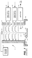
- a particle beam device such as a scanning electron microscope 7, shown in Figure 1, includes a voltage source 11.
- the voltage source 11 is connected to an electron source 13 that directs a narrow beam of highly accelerated electrons towards a specimen stage 18 via a plurality of electron lenses L 1 , L 2 , and L 3 .
- the electron beam is indicated by the dashed line 14.
- the electron beam may be focused onto a wafer stage of the scanning electron microscope using an autofocus technique.
- a cylindrical column 17 houses the electron source 13 and the lenses L 1 , L 2 , and L 3 .
- the column 17 is normally referred to as an electron optical column and includes a chamber, indicated in the drawing as 17A, that surrounds and supports a specimen stage 18. Together, the optical column 17 and the chamber 17A represent the body of the scanning electron microscope.
- the scanning electron microscope 7 of Figure 1 further includes an electromagnetic or electrostatic deflection system for selectively scanning the electron beam across the specimen stage 18.
- the deflection system includes four pairs of electron beam scanning coils, designated D 1 trough D 4 .
- the scanning coils are located within optical column 17 for focusing the electron beam on the surface of the specimen held on stage 18.
- the pair of deflection coils D 1 and D 2 are connected to sawtooth voltage generator 19, and the pair of deflection coils D 3 and D 4 are connected to sawtooth voltage generator 20.
- the electron beam scanning coils D 1 through D 4 deflect the electron beam 14 in two, generally perpendicular, directions.
- the deflection directions are designated as the x-direction and the y-direction, respectively.
- the x-direction and the y-direction typically are in a plane perpendicular to the direction of beam 14, but strict orthogonality is not required.
- coils D 1 and D 3 deflect the scanning beam in the x-direction and that coils D 2 and D 4 deflect the scanning beam in the y-direction.
- An electron collector 22 is arranged near the surface of a stage 18 which is exposed to beam 14.
- the electron collector is connected to an amplifier 23 which provides signals to an analog-to-digital converter 43 for transforming the collected electron current to digital signals which may be subsequently displayed on a video display 49.
- saw-tooth generators 19 and 20 provide time-varying voltage signals to electron beam scanning coils D 1 and D 4 such that beam 14 is deflected across specimen stage 18 in a predetermined scanning pattern.
- the saw-tooth generators 19 and 20 typically operate synchronously to drive the electron beam across stage 18 in the x-direction at a constant rate, with each scan beam deflected in the y-direction to form a series of generally parallel scanning lines.
- collector 22 detects changes in the electron current at stage 18.
- the electron beams scans a specimen on stage 18
- changes in the composition, texture and topography of the specimen causing amplitude variations of the electron current detected by collector 22.
- an image corresponding to features of the specimen can be created.
- Such a high-aspect-ratio contact hole is a common feature of semiconductor wafers and is shown in Figure 2.
- a layer of resist 31 has been used to pattern a sub-micrometer contact hole in a layer of oxide 33 coated on the surface of a wafer 35.
- the height h of the contact hole is considerably greater than the width w of the contact hole such that h/w > > 1.
- Typical values of h and w might be 2.0 ⁇ m and 0.5 ⁇ m respectively, giving an aspect ratio of 4:1.
- the present invention provides improved imaging techniques for imaging high-aspect-ratio structures such as contact holes. These techniques represent a departure from conventional approaches to this class of imaging problems.
- the new approach utilizes two signal detection sub-systems, one optimized for imaging at the top and another optimized for imaging at the base of sub-micrometer structures. These detection systems produce signals that can be combined in real-time to produce an image which resembles the "extended focus" images obtained with confocal optical microscopes. Unlike the confocal image, however, the resulting image has the inherent linearity and resolution characteristics of electron-beam technology.
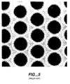
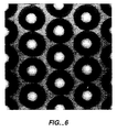
- FIG. 6 shows an example of an base-biased image.
- the structures are 0.5 ⁇ m nominal contacts to silicon which are developed and etched into a 2.0 ⁇ m-thick layer of resist on oxide.
- the bottom of the contact hole is clearly visible as a white circle.
- image information corresponding to features near a base of a microscopic high-aspect-ratio structure is extracted by directing a primary electron beam onto the structure and discriminating between high-energy and low-energy backscatter electrons emitted from the structure as a result of the primary electron beam being directed onto the structure.
- a detector high-energy backscatter electrons are detected to produce a detection signal, and the detection signal is used to produce an image corresponding to features near the base of the structure.
- an imaging device includes a stage for supporting a wafer on which a microscopic structure is patterned, a mechanism for directing a primary electron beam onto the microscopic structure, a mechanism for discriminating between high-energy backscatter electrons and low-energy backscatter electrons emitted from the structure as a result of the primary electron beam being directed onto the structure, a detector for detecting high-energy backscatter electrons to produce a detection signal, and an imaging device responsive to the detection signal for producing an image of the structure.
- high-aspect-ratio structures such as microelectronic contact holes may be imaged using two signal detection subsystems, one optimized for imaging at the top and another optimized for imaging at the base of sub-micrometer structures.
- both detectors are of a microchannel plate detectors of a type well-known in the art.
- the detector furthest removed from the object being imaged will be referred to as the upper detector (UD), and the detector closest to the object being imaged will be referred to as the lower detector (LD).
- the imaging geometry associated with the lower detector is best adapted for imaging the top surface of the object
- the imaging geometry associated with the upper detector is best adapted for imaging at the base of troughs and holes.
- the lower detector receives backscatter emission of electrons in a solid angle defined by ⁇ 1 , ⁇ 2 where ⁇ 1 is near 90° from the normal to the sample and ⁇ 2 is near 45° from the normal, so that the resulting signal is dominated by electrons from the top surface.
- the upper detector receives backscatter electrons in a solid angle described by ⁇ 3 , ⁇ 4 where ⁇ 3 is less than 45° and ⁇ 4 is near 0°, so that the resulting signal is dominated by electrons from holes and trenches.
- a magnetic field-immersion objective lens may be used to accomplish adjustment of ⁇ 1 , ⁇ 2 , ⁇ 3 and ⁇ 4 .
- the geometry of Figure 7 accomplishes a spatial filtering whereby backscattered electrons and secondary emission electrons are discriminated from one another and imaged on the upper and lower detectors, respectively, to achieve top and base biased imaging.
- the lower detector is positioned inside an immersion electromagnetic lens
- the upper detector is positioned above the immersion electromagnetic lens.
- the spatial filtering effect of the geometry illustrated in Figure 7 may be augmented by energy filtering to prevent secondary electrons from being imaged on the upper detector.
- the face of the upper detector is negatively biased (for example, to about -300 volts) so as to repel the low-energy secondary electrons.
- the backscattered electrons are of sufficiently high energy so as to remain substantially unaffected by the negative bias.
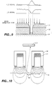
- the signal from the lower detector is at a near-zero minimum when the base of the structure is being scanned, whereas the signal from the upper detector exhibits its maximum at the base of the structure, allowing high-precision measurement with no need for extrapolation.
- the primary electron beam is scanned across the cross-section shown in Figure 9 in a left to right direction.
- an abundance of electrons are emitted so as to strike the lower detector and produce a high level signal.
- Surface charge effects do not appreciably influence the signal.
- the influence of surface charge effects increases.
- the signal from the lower detector therefore falls to a near-zero minimum.
- the signal from the lower detector again rises to a high level.
- the signal from the upper detector exhibits exactly the opposite behavior.
- Backscattered electron yield increases with the atomic number of the material on which the primary electron beams lands.
- Photoresist compositions in general have a relatively low atomic number, whereas silicon has a relatively high atomic number.
- As the surface of the structure is being scanned relatively few backscattered electrons are produced.
- As the primary electron beam scans the bottom of the contact hole large numbers of backscattered electrons are produced because of the high atomic number of silicon.
- This reverse image contrast is further assisted by the small acceptance angle of the upper detector, which reduces the unwanted signal from laterally scattered electrons emitted at the top surface of the structure.
- the electrons are emitted in all directions. Within a contact hole, or other high aspect ratio structure, however, the electrons are subject to a collimating effect produced by the structure. Because of the small angle of acceptance of the upper detector, the latter "collimated" electrons are received on the upper detector in greater proportion than the former "undirected" surface electrons.
- the SE signal varies with surface topography, depends very heavily on the incident beam energy and current, and is sensitive to surface charging.
- Collection efficiency of backscattered electrons may be further increased by providing a negative electron optical working distance for the scanning electron microscope.
- an electromagnetic immersion objective of the scanning electron microscope is principally composed of a toroidal, channel-shaped magnetic polepiece 39 and an electric winding 41 wound inside the channel of the polepiece.
- the electromagnetic immersion lens produces a magnetic flux pattern as shown.
- the magnetic flux pattern is precisely controlled in such a way as to compensate for aberrations.
- the electron-optical working distance is typically positive.
- the electron-optical working distance refers to the distance between the surface plane of the wafer (43) and a plane corresponding to a region of maximum flux density (45). In a preferred embodiment, this distance is slightly negative (approximately -1mm).
- the plane of the wafer surface (43) is positioned above a plane (45) corresponding to a region of maximum flux density.
- the effect of this slightly negative electron-optical working distance is to sweep backscattered electrons onto channel plates of the upper and lower detectors.
- a negative electron optical working distance causes backscattered electrons to strike the detectors even when the electrons are emitted at a significant angle from normal. Since backscattered electrons are low-yield, the resulting increase in collection efficiency is of considerable significance.
- FIG 11 shows in detail the electron column of a scanning electron microscope according to a preferred embodiment of the present invention.
- the electron beam path is represented by a vertical broken line 47 and extends down to the wafer plane 43.
- An upper octupole assembly 49 functions to position the electron beam.
- An upper detector assembly 51 houses the upper detector, preferably a microchannel plate detector.
- a magnetic lens liner 55 is a tellurium copper shield that protects the beam from disturbances that might otherwise be created by eight teflon-coated wires used to control the octupole. It also holds the octupole in place.
- a lower octupole assembly 57 functions to scan the electron beam back and forth across the surface of the wafer. The lower detector opposes the wafer surface and is preferably a microchannel plate detector.
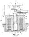
- Figure 12 shows the complete electron optics of a scanning electron microscope according to a preferred embodiment of the invention.
- An upper column assembly 60 houses the upper octupole, the spray aperture assembly 50 and the upper detector assembly 51 and includes an electron gun interface 46.
- a magnetic lens assembly 70 includes a magnetic lens pole-piece 39 and electric winding 41. Attached to the polepiece is a lens cap 71. The magnetic lens liner extends inside the magnetic lens assembly 70. Also housed inside the magnetic lens assembly 70 are the lower octupole assembly 57 and the lower detector.
- the signals from the upper and lower detectors need not be used in exclusion to one another.
- the signals from the upper and lower detectors are combined in a variable ratio in accordance with a control arrangement to produce an image resembling an "extended focus" image.
- the signals may be combined in real time to produce a mixed-signal image having the inherent linearity and resolution characteristic of electron-beam technology.
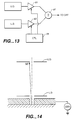
- signals from the upper and lower detectors are input to variable-gain amplifiers 81 and 83, respectively.
- the gains of the amplifiers are set in accordance with control signals from a control unit 85.
- the output signals from the amplifiers are then summed in a summer 87, the output of which is sent to the CRT display.
- the beam current may be lowered and the upper detector may advantageously be used to detect secondary electrons instead of backscattered electrons as previously described. Lowering the beam current reduces surface charging, improving resolution and measurement precision in the case of highly insulated materials.
- the capability to observe the bottom of high aspect ratio structures (such as trenches) is preserved under conditions as shown in Figure 14.
- the collection of secondary electrons at the upper detector is facilitated by applying a bias voltage of about -160V to the wafer.
- the face of the upper detector instead of being negatively biased as before, is now unbiased. Secondary electrons are accelerated pushed up the column to the upper detector, where they exhibit trajectories more similar to those of backscattered electrons.
Landscapes
- Chemical & Material Sciences (AREA)
- Analytical Chemistry (AREA)
- Testing Or Measuring Of Semiconductors Or The Like (AREA)
- Length-Measuring Devices Using Wave Or Particle Radiation (AREA)
- Investigating Or Analyzing Materials By The Use Of Fluid Adsorption Or Reactions (AREA)
- Investigating Or Analysing Materials By The Use Of Chemical Reactions (AREA)
- Developing Agents For Electrophotography (AREA)
- Glass Compositions (AREA)
- Optical Radar Systems And Details Thereof (AREA)
- Investigating Or Analysing Materials By Optical Means (AREA)
- Analysing Materials By The Use Of Radiation (AREA)
Abstract
Description
Claims (10)
- A method of extracting image information corresponding to features near a base of a microscopic high-aspect-ratio structure using an electron beam device having a detection aperture, comprising the steps of:directing a primary electron beam onto said structure;discriminating between high-energy and low-energy backscatter electrons emitted from said structure as a result of said primary electron beam being directed onto said structure;using a detector, detecting said low-energy backscatter electrons to produce a detection signal; andusing said detection signal to produce an image corresponding to features near the base of said structure.
- The method of claim 1 wherein said discriminating step comprises locating said detector relative to said detection aperture and an upper surface of said structure such that said detector subtends an angle having a vertex at a level of said upper surface of said structure, said angle extending no more than 45° on either side of a normal to said upper surface of said structure.
- An apparatus for inspecting and/or measuring wafer structures, comprising:stage means for supporting a wafer on which a microscopic structure is patterned;means for directing a primary electron beam onto said microscopic structure;means for discriminating between high-energy backscatter electrons and low-energy backscatter electrons emitted from said structure as a result of said primary electron beam being directed onto said structure;first detector means for detecting said low-energy backscatter electrons to produce a first detection signal; andimaging means responsive at least in part to said first detection signal for producing an image of said structure.
- The apparatus of claim 3, further comprising:second detector means for detecting said high-energy backscatter electrons to produce a second detection signal; andmixing means for mixing said first and second detection signals in variable proportion to one another to produce a mixed detection signal;wherein said imaging means is responsive to said mixed detection signal for producing an image of said structure.
- The apparatus of claim 4, wherein said first and second detector means are first and second micro channel plate detectors each having a central primary electron beam exposure aperture.
- The apparatus of claim 5 wherein said first micro channel plate detector is disposed above said second micro channel plate detector with beam exposure apertures of said micro channel plate detectors being vertically aligned.
- The apparatus of claim 6 wherein said beam exposure aperture of said second micro channel plate detector functions as a detection aperture for said first micro channel plate detector.
- The apparatus of claim 7 wherein said stage, said second micro channel plate detector, and said first micro channel plate detector are positioned relative to one another such that said first micro channel plate detector subtends an angle having a vertex at a level of an upper surface of said structure, an angle extending no more than 45° on either side of a normal to said upper surface of said structure.
- The apparatus of claim 8, further comprising magnetic lens means for focussing said electrons on said detectors.
- The apparatus of claim 9 wherein said stage means and said magnetic lens means are located relative to one another such that said wafer is located at a negative electron-optical working distance, causing said high-energy backscatter electrons to impinge said first micro channel plate detector at a significant angle from the normal.
Applications Claiming Priority (3)
| Application Number | Priority Date | Filing Date | Title |
|---|---|---|---|
| US08/141,669 US5493116A (en) | 1993-10-26 | 1993-10-26 | Detection system for precision measurements and high resolution inspection of high aspect ratio structures using particle beam devices |
| US141669 | 1993-10-26 | ||
| PCT/US1994/011602 WO1995012210A1 (en) | 1993-10-26 | 1994-10-12 | Detection system for measuring high aspect ratio |
Publications (3)
| Publication Number | Publication Date |
|---|---|
| EP0725975A1 EP0725975A1 (en) | 1996-08-14 |
| EP0725975A4 EP0725975A4 (en) | 1997-12-29 |
| EP0725975B1 true EP0725975B1 (en) | 2000-01-26 |
Family
ID=22496687
Family Applications (1)
| Application Number | Title | Priority Date | Filing Date |
|---|---|---|---|
| EP94930746A Expired - Lifetime EP0725975B1 (en) | 1993-10-26 | 1994-10-12 | Detection system for measuring high aspect ratio |
Country Status (8)
| Country | Link |
|---|---|
| US (1) | US5493116A (en) |
| EP (1) | EP0725975B1 (en) |
| JP (1) | JP3456999B2 (en) |
| AT (1) | ATE189336T1 (en) |
| AU (1) | AU7977494A (en) |
| DE (1) | DE69422825T2 (en) |
| IL (1) | IL111384A (en) |
| WO (1) | WO1995012210A1 (en) |
Families Citing this family (37)
| Publication number | Priority date | Publication date | Assignee | Title |
|---|---|---|---|---|
| US5866904A (en) * | 1990-10-12 | 1999-02-02 | Hitachi, Ltd. | Scanning electron microscope and method for dimension measuring by using the same |
| US6066849A (en) * | 1997-01-16 | 2000-05-23 | Kla Tencor | Scanning electron beam microscope |
| US5995867A (en) | 1997-03-19 | 1999-11-30 | Lucid Inc | Cellular surgery utilizing confocal microscopy |
| JPH1167139A (en) * | 1997-08-25 | 1999-03-09 | Hitachi Ltd | Scanning electron microscope |
| US6274393B1 (en) | 1998-04-20 | 2001-08-14 | International Business Machines Corporation | Method for measuring submicron images |
| TW402769B (en) * | 1998-06-13 | 2000-08-21 | Samsung Electronics Co Ltd | Apparatus and method for contact failure inspection in semiconductor devices |
| GB2341720A (en) * | 1998-09-16 | 2000-03-22 | Leica Microsys Lithography Ltd | Electron beam aperture element with beam sheilding |
| US6539106B1 (en) | 1999-01-08 | 2003-03-25 | Applied Materials, Inc. | Feature-based defect detection |
| US6344750B1 (en) | 1999-01-08 | 2002-02-05 | Schlumberger Technologies, Inc. | Voltage contrast method for semiconductor inspection using low voltage particle beam |
| US6232787B1 (en) | 1999-01-08 | 2001-05-15 | Schlumberger Technologies, Inc. | Microstructure defect detection |
| US6252412B1 (en) | 1999-01-08 | 2001-06-26 | Schlumberger Technologies, Inc. | Method of detecting defects in patterned substrates |
| US6414308B1 (en) | 1999-03-12 | 2002-07-02 | International Business Machines Corporation | Method for determining opened/unopened semiconductor contacts using a scanning electron microscope |
| KR100546289B1 (en) | 1999-04-23 | 2006-01-26 | 삼성전자주식회사 | In-line monitoring method of contact hole using electron beam inspection device |
| US6586733B1 (en) | 1999-05-25 | 2003-07-01 | Kla-Tencor | Apparatus and methods for secondary electron emission microscope with dual beam |
| US6545491B2 (en) | 1999-08-27 | 2003-04-08 | Samsung Electronics Co., Ltd. | Apparatus for detecting defects in semiconductor devices and methods of using the same |
| US6642150B1 (en) | 1999-12-28 | 2003-11-04 | Taiwan Semiconductor Manufacturing Company | Method for testing for blind hole formed in wafer layer |
| US6847038B2 (en) * | 2002-07-15 | 2005-01-25 | Hitachi, Ltd. | Scanning electron microscope |
| DE60042758D1 (en) | 2000-03-31 | 2009-09-24 | Hitachi Ltd | SENSE ELECTRON MICROSCOPE |
| WO2002001597A1 (en) * | 2000-06-27 | 2002-01-03 | Ebara Corporation | Charged particle beam inspection apparatus and method for fabricating device using that inspection apparatus |
| US6548810B2 (en) * | 2001-08-01 | 2003-04-15 | The University Of Chicago | Scanning confocal electron microscope |
| DE10230929A1 (en) * | 2002-07-09 | 2004-01-29 | Leo Elektronenmikroskopie Gmbh | Method for electron microscopic observation of a semiconductor device and device therefor |
| US7528614B2 (en) * | 2004-12-22 | 2009-05-05 | Applied Materials, Inc. | Apparatus and method for voltage contrast analysis of a wafer using a tilted pre-charging beam |
| US6797955B1 (en) | 2003-01-30 | 2004-09-28 | Kla-Tencor Technologies Corporation | Filtered e-beam inspection and review |
| US6812462B1 (en) | 2003-02-21 | 2004-11-02 | Kla-Tencor Technologies Corporation | Dual electron beam instrument for multi-perspective |
| US6815675B1 (en) | 2003-04-30 | 2004-11-09 | Kla-Tencor Technologies Corporation | Method and system for e-beam scanning |
| US7019292B1 (en) | 2004-06-15 | 2006-03-28 | Kla-Tencor Technologies Corporation | E-beam detection of defective contacts/vias with flooding and energy filter |
| US7241991B1 (en) | 2005-08-30 | 2007-07-10 | Kla-Tencor Technologies Corporation | Region-of-interest based electron beam metrology |
| JP5054990B2 (en) * | 2007-01-30 | 2012-10-24 | 株式会社日立ハイテクノロジーズ | Scanning electron microscope |
| JP2010175249A (en) * | 2009-01-27 | 2010-08-12 | Hitachi High-Technologies Corp | Method and device for measuring height of sample |
| JP6035928B2 (en) * | 2012-07-12 | 2016-11-30 | 株式会社日立ハイテクノロジーズ | Charged particle beam equipment |
| US9786468B2 (en) * | 2013-02-26 | 2017-10-10 | Hitachi High-Technologies Corporation | Charged particle beam device |
| JP6581940B2 (en) * | 2016-04-15 | 2019-09-25 | 株式会社日立ハイテクノロジーズ | Electron microscope equipment |
| US10096447B1 (en) * | 2017-08-02 | 2018-10-09 | Kla-Tencor Corporation | Electron beam apparatus with high resolutions |
| JP2019169406A (en) | 2018-03-26 | 2019-10-03 | 株式会社日立ハイテクノロジーズ | Charged particle beam apparatus |
| DE102018204683B3 (en) * | 2018-03-27 | 2019-08-08 | Carl Zeiss Microscopy Gmbh | electron microscope |
| JP7396954B2 (en) * | 2020-04-01 | 2023-12-12 | 株式会社日立ハイテク | Charged particle beam device |
| US11626267B2 (en) * | 2021-04-28 | 2023-04-11 | Applied Materials Israel Ltd. | Back-scatter electrons (BSE) imaging with a SEM in tilted mode using cap bias voltage |
Family Cites Families (9)
| Publication number | Priority date | Publication date | Assignee | Title |
|---|---|---|---|---|
| JPS5927075B2 (en) * | 1974-07-17 | 1984-07-03 | ユニチカ株式会社 | Scanning electron microscope |
| JPS5481075A (en) * | 1977-11-24 | 1979-06-28 | Cho Lsi Gijutsu Kenkyu Kumiai | Method of detecting article image using electron beam |
| JPS59197881A (en) * | 1983-04-25 | 1984-11-09 | Jeol Ltd | Reflected electron detecting device having energy selecting function |
| US4588890A (en) * | 1984-12-31 | 1986-05-13 | International Business Machines Corporation | Apparatus and method for composite image formation by scanning electron beam |
| US4868344A (en) * | 1988-03-30 | 1989-09-19 | Aldrich-Boranes, Inc. | Novel process of producing phenyl or substituted phenylalkylamine pharmaceutical agents and novel chiral intermediates of high enantiomeric purity useful therein |
| US4958079A (en) * | 1989-02-21 | 1990-09-18 | Galileo Electro-Optics Corps. | Detector for scanning electron microscopy apparatus |
| JPH0467550A (en) * | 1990-07-05 | 1992-03-03 | Fujitsu Ltd | Electron beam device and image extracting method thereof |
| JP3285092B2 (en) * | 1990-10-12 | 2002-05-27 | 株式会社日立製作所 | Scanning electron microscope and sample image forming method using scanning electron microscope |
| US5332898A (en) * | 1993-06-14 | 1994-07-26 | Metrologix | Precision measurement using particle beam devices |
-
1993
- 1993-10-26 US US08/141,669 patent/US5493116A/en not_active Expired - Lifetime
-
1994
- 1994-10-12 JP JP51266595A patent/JP3456999B2/en not_active Expired - Lifetime
- 1994-10-12 AU AU79774/94A patent/AU7977494A/en not_active Abandoned
- 1994-10-12 EP EP94930746A patent/EP0725975B1/en not_active Expired - Lifetime
- 1994-10-12 DE DE69422825T patent/DE69422825T2/en not_active Expired - Lifetime
- 1994-10-12 WO PCT/US1994/011602 patent/WO1995012210A1/en not_active Ceased
- 1994-10-12 AT AT94930746T patent/ATE189336T1/en not_active IP Right Cessation
- 1994-10-24 IL IL11138494A patent/IL111384A/en not_active IP Right Cessation
Also Published As
| Publication number | Publication date |
|---|---|
| ATE189336T1 (en) | 2000-02-15 |
| US5493116A (en) | 1996-02-20 |
| DE69422825T2 (en) | 2000-08-17 |
| IL111384A (en) | 1998-07-15 |
| AU7977494A (en) | 1995-05-22 |
| IL111384A0 (en) | 1994-12-29 |
| WO1995012210A1 (en) | 1995-05-04 |
| DE69422825D1 (en) | 2000-03-02 |
| JPH09507331A (en) | 1997-07-22 |
| EP0725975A4 (en) | 1997-12-29 |
| EP0725975A1 (en) | 1996-08-14 |
| JP3456999B2 (en) | 2003-10-14 |
Similar Documents
| Publication | Publication Date | Title |
|---|---|---|
| US5493116A (en) | Detection system for precision measurements and high resolution inspection of high aspect ratio structures using particle beam devices | |
| US5302828A (en) | Scanning techniques in particle beam devices for reducing the effects of surface charge accumulation | |
| US6605805B2 (en) | Swinging objective retarding immersion lens electron optics focusing, deflection and signal collection system and method | |
| US6218664B1 (en) | SEM provided with an electrostatic objective and an electrical scanning device | |
| US7399966B2 (en) | Scanning electron microscope | |
| US7075078B2 (en) | Scanning electron microscope | |
| EP1238405B1 (en) | Method and system for the examination of specimen using a charged particle beam | |
| EP0661727A2 (en) | Scanning electron microscope | |
| US6960766B2 (en) | Swinging objective retarding immersion lens electron optics focusing, deflection and signal collection system and method | |
| EP0113746B1 (en) | An elektrode system of a retarding-field spectrometer for a voltage measuring electron beam apparatus | |
| US6646261B2 (en) | SEM provided with a secondary electron detector having a central electrode | |
| US20020109089A1 (en) | SEM provided with an adjustable final electrode in the electrostatic objective | |
| US7800062B2 (en) | Method and system for the examination of specimen | |
| US7218126B2 (en) | Inspection method and apparatus for circuit pattern | |
| JP2005521215A (en) | Electro-optical focusing, deflection, signal acquisition system and method for swinging objective decelerating immersion lens | |
| WO1996008835A1 (en) | Particle beam detector providing z-axis and topographic contrast | |
| EP0425204A2 (en) | Secondary ion mass analyzing apparatus | |
| US7335879B2 (en) | System and method for sample charge control | |
| US20020079449A1 (en) | SEM having a detector surface segmented into a number of separate regions | |
| IL108349A (en) | Scanning techniques in particle beam devices for reducing the effects of surface charge accumulation |
Legal Events
| Date | Code | Title | Description |
|---|---|---|---|
| PUAI | Public reference made under article 153(3) epc to a published international application that has entered the european phase |
Free format text: ORIGINAL CODE: 0009012 |
|
| 17P | Request for examination filed |
Effective date: 19960429 |
|
| AK | Designated contracting states |
Kind code of ref document: A1 Designated state(s): AT BE CH DE DK ES FR GB GR IE IT LI LU MC NL PT SE |
|
| A4 | Supplementary search report drawn up and despatched |
Effective date: 19971104 |
|
| AK | Designated contracting states |
Kind code of ref document: A4 Designated state(s): AT BE CH DE DK ES FR GB GR IE IT LI LU MC NL PT SE |
|
| GRAG | Despatch of communication of intention to grant |
Free format text: ORIGINAL CODE: EPIDOS AGRA |
|
| 17Q | First examination report despatched |
Effective date: 19990104 |
|
| GRAG | Despatch of communication of intention to grant |
Free format text: ORIGINAL CODE: EPIDOS AGRA |
|
| GRAH | Despatch of communication of intention to grant a patent |
Free format text: ORIGINAL CODE: EPIDOS IGRA |
|
| GRAH | Despatch of communication of intention to grant a patent |
Free format text: ORIGINAL CODE: EPIDOS IGRA |
|
| GRAA | (expected) grant |
Free format text: ORIGINAL CODE: 0009210 |
|
| AK | Designated contracting states |
Kind code of ref document: B1 Designated state(s): AT BE CH DE DK ES FR GB GR IE IT LI LU MC NL PT SE |
|
| PG25 | Lapsed in a contracting state [announced via postgrant information from national office to epo] |
Ref country code: SE Free format text: THE PATENT HAS BEEN ANNULLED BY A DECISION OF A NATIONAL AUTHORITY Effective date: 20000126 Ref country code: NL Free format text: LAPSE BECAUSE OF FAILURE TO SUBMIT A TRANSLATION OF THE DESCRIPTION OR TO PAY THE FEE WITHIN THE PRESCRIBED TIME-LIMIT Effective date: 20000126 Ref country code: LI Free format text: LAPSE BECAUSE OF FAILURE TO SUBMIT A TRANSLATION OF THE DESCRIPTION OR TO PAY THE FEE WITHIN THE PRESCRIBED TIME-LIMIT Effective date: 20000126 Ref country code: IT Free format text: LAPSE BECAUSE OF FAILURE TO SUBMIT A TRANSLATION OF THE DESCRIPTION OR TO PAY THE FEE WITHIN THE PRESCRIBED TIME-LIMIT;WARNING: LAPSES OF ITALIAN PATENTS WITH EFFECTIVE DATE BEFORE 2007 MAY HAVE OCCURRED AT ANY TIME BEFORE 2007. THE CORRECT EFFECTIVE DATE MAY BE DIFFERENT FROM THE ONE RECORDED. Effective date: 20000126 Ref country code: GR Free format text: LAPSE BECAUSE OF NON-PAYMENT OF DUE FEES Effective date: 20000126 Ref country code: FR Free format text: LAPSE BECAUSE OF FAILURE TO SUBMIT A TRANSLATION OF THE DESCRIPTION OR TO PAY THE FEE WITHIN THE PRESCRIBED TIME-LIMIT Effective date: 20000126 Ref country code: ES Free format text: THE PATENT HAS BEEN ANNULLED BY A DECISION OF A NATIONAL AUTHORITY Effective date: 20000126 Ref country code: CH Free format text: LAPSE BECAUSE OF FAILURE TO SUBMIT A TRANSLATION OF THE DESCRIPTION OR TO PAY THE FEE WITHIN THE PRESCRIBED TIME-LIMIT Effective date: 20000126 Ref country code: BE Free format text: LAPSE BECAUSE OF FAILURE TO SUBMIT A TRANSLATION OF THE DESCRIPTION OR TO PAY THE FEE WITHIN THE PRESCRIBED TIME-LIMIT Effective date: 20000126 Ref country code: AT Free format text: LAPSE BECAUSE OF FAILURE TO SUBMIT A TRANSLATION OF THE DESCRIPTION OR TO PAY THE FEE WITHIN THE PRESCRIBED TIME-LIMIT Effective date: 20000126 |
|
| REF | Corresponds to: |
Ref document number: 189336 Country of ref document: AT Date of ref document: 20000215 Kind code of ref document: T |
|
| REG | Reference to a national code |
Ref country code: CH Ref legal event code: EP |
|
| REF | Corresponds to: |
Ref document number: 69422825 Country of ref document: DE Date of ref document: 20000302 |
|
| REG | Reference to a national code |
Ref country code: IE Ref legal event code: FG4D |
|
| PG25 | Lapsed in a contracting state [announced via postgrant information from national office to epo] |
Ref country code: PT Free format text: LAPSE BECAUSE OF FAILURE TO SUBMIT A TRANSLATION OF THE DESCRIPTION OR TO PAY THE FEE WITHIN THE PRESCRIBED TIME-LIMIT Effective date: 20000426 Ref country code: DK Free format text: LAPSE BECAUSE OF FAILURE TO SUBMIT A TRANSLATION OF THE DESCRIPTION OR TO PAY THE FEE WITHIN THE PRESCRIBED TIME-LIMIT Effective date: 20000426 |
|
| EN | Fr: translation not filed | ||
| NLV1 | Nl: lapsed or annulled due to failure to fulfill the requirements of art. 29p and 29m of the patents act | ||
| REG | Reference to a national code |
Ref country code: CH Ref legal event code: PL |
|
| PG25 | Lapsed in a contracting state [announced via postgrant information from national office to epo] |
Ref country code: LU Free format text: LAPSE BECAUSE OF NON-PAYMENT OF DUE FEES Effective date: 20001012 Ref country code: IE Free format text: LAPSE BECAUSE OF NON-PAYMENT OF DUE FEES Effective date: 20001012 |
|
| PG25 | Lapsed in a contracting state [announced via postgrant information from national office to epo] |
Ref country code: MC Free format text: THE PATENT HAS BEEN ANNULLED BY A DECISION OF A NATIONAL AUTHORITY Effective date: 20001031 |
|
| PLBE | No opposition filed within time limit |
Free format text: ORIGINAL CODE: 0009261 |
|
| STAA | Information on the status of an ep patent application or granted ep patent |
Free format text: STATUS: NO OPPOSITION FILED WITHIN TIME LIMIT |
|
| 26N | No opposition filed | ||
| REG | Reference to a national code |
Ref country code: IE Ref legal event code: MM4A |
|
| REG | Reference to a national code |
Ref country code: GB Ref legal event code: IF02 |
|
| PGFP | Annual fee paid to national office [announced via postgrant information from national office to epo] |
Ref country code: DE Payment date: 20131029 Year of fee payment: 20 Ref country code: GB Payment date: 20131028 Year of fee payment: 20 |
|
| REG | Reference to a national code |
Ref country code: DE Ref legal event code: R071 Ref document number: 69422825 Country of ref document: DE |
|
| REG | Reference to a national code |
Ref country code: DE Ref legal event code: R071 Ref document number: 69422825 Country of ref document: DE |
|
| REG | Reference to a national code |
Ref country code: GB Ref legal event code: PE20 Expiry date: 20141011 |
|
| PG25 | Lapsed in a contracting state [announced via postgrant information from national office to epo] |
Ref country code: GB Free format text: LAPSE BECAUSE OF EXPIRATION OF PROTECTION Effective date: 20141011 |
|
| P01 | Opt-out of the competence of the unified patent court (upc) registered |
Effective date: 20230525 |