EP0721108B1 - Acceleration condition sensor apparatus - Google Patents
Acceleration condition sensor apparatus Download PDFInfo
- Publication number
- EP0721108B1 EP0721108B1 EP95309044A EP95309044A EP0721108B1 EP 0721108 B1 EP0721108 B1 EP 0721108B1 EP 95309044 A EP95309044 A EP 95309044A EP 95309044 A EP95309044 A EP 95309044A EP 0721108 B1 EP0721108 B1 EP 0721108B1
- Authority
- EP
- European Patent Office
- Prior art keywords
- substrate
- housing
- bottom wall
- blade member
- sidewall
- Prior art date
- Legal status (The legal status is an assumption and is not a legal conclusion. Google has not performed a legal analysis and makes no representation as to the accuracy of the status listed.)
- Expired - Lifetime
Links
- 230000001133 acceleration Effects 0.000 title claims description 40
- 239000000758 substrate Substances 0.000 claims description 72
- 239000003990 capacitor Substances 0.000 claims description 10
- 230000004044 response Effects 0.000 claims description 6
- 239000012858 resilient material Substances 0.000 claims description 5
- 230000007613 environmental effect Effects 0.000 claims description 4
- 238000007789 sealing Methods 0.000 claims 1
- 239000000463 material Substances 0.000 description 14
- 229910052751 metal Inorganic materials 0.000 description 10
- 239000002184 metal Substances 0.000 description 10
- 230000003750 conditioning effect Effects 0.000 description 5
- 239000011521 glass Substances 0.000 description 5
- 239000000956 alloy Substances 0.000 description 4
- 229910045601 alloy Inorganic materials 0.000 description 4
- PNEYBMLMFCGWSK-UHFFFAOYSA-N aluminium oxide Inorganic materials [O-2].[O-2].[O-2].[Al+3].[Al+3] PNEYBMLMFCGWSK-UHFFFAOYSA-N 0.000 description 4
- 238000000034 method Methods 0.000 description 4
- 230000009977 dual effect Effects 0.000 description 3
- 239000003566 sealing material Substances 0.000 description 3
- 229910000679 solder Inorganic materials 0.000 description 3
- 238000003466 welding Methods 0.000 description 3
- XEEYBQQBJWHFJM-UHFFFAOYSA-N Iron Chemical compound [Fe] XEEYBQQBJWHFJM-UHFFFAOYSA-N 0.000 description 2
- PXHVJJICTQNCMI-UHFFFAOYSA-N Nickel Chemical compound [Ni] PXHVJJICTQNCMI-UHFFFAOYSA-N 0.000 description 2
- 230000002411 adverse Effects 0.000 description 2
- 239000011248 coating agent Substances 0.000 description 2
- 238000000576 coating method Methods 0.000 description 2
- 238000004806 packaging method and process Methods 0.000 description 2
- 230000035945 sensitivity Effects 0.000 description 2
- 239000004593 Epoxy Substances 0.000 description 1
- 229920000106 Liquid crystal polymer Polymers 0.000 description 1
- 239000004977 Liquid-crystal polymers (LCPs) Substances 0.000 description 1
- 239000004642 Polyimide Substances 0.000 description 1
- 229910000831 Steel Inorganic materials 0.000 description 1
- 238000005452 bending Methods 0.000 description 1
- 238000004891 communication Methods 0.000 description 1
- 239000000356 contaminant Substances 0.000 description 1
- 229910052593 corundum Inorganic materials 0.000 description 1
- 230000008878 coupling Effects 0.000 description 1
- 238000010168 coupling process Methods 0.000 description 1
- 238000005859 coupling reaction Methods 0.000 description 1
- 230000003247 decreasing effect Effects 0.000 description 1
- 229920001971 elastomer Polymers 0.000 description 1
- 239000013536 elastomeric material Substances 0.000 description 1
- 239000012777 electrically insulating material Substances 0.000 description 1
- 230000004907 flux Effects 0.000 description 1
- 238000009434 installation Methods 0.000 description 1
- 229910052742 iron Inorganic materials 0.000 description 1
- 238000004519 manufacturing process Methods 0.000 description 1
- 238000002844 melting Methods 0.000 description 1
- 230000008018 melting Effects 0.000 description 1
- 239000000203 mixture Substances 0.000 description 1
- 238000012986 modification Methods 0.000 description 1
- 230000004048 modification Effects 0.000 description 1
- 229910052759 nickel Inorganic materials 0.000 description 1
- TWNQGVIAIRXVLR-UHFFFAOYSA-N oxo(oxoalumanyloxy)alumane Chemical compound O=[Al]O[Al]=O TWNQGVIAIRXVLR-UHFFFAOYSA-N 0.000 description 1
- 229920001721 polyimide Polymers 0.000 description 1
- 229920001296 polysiloxane Polymers 0.000 description 1
- 230000008569 process Effects 0.000 description 1
- 230000001681 protective effect Effects 0.000 description 1
- 238000007650 screen-printing Methods 0.000 description 1
- 230000035939 shock Effects 0.000 description 1
- 229920002379 silicone rubber Polymers 0.000 description 1
- 239000004945 silicone rubber Substances 0.000 description 1
- 239000010959 steel Substances 0.000 description 1
- 229910001845 yogo sapphire Inorganic materials 0.000 description 1
Images


Classifications
-
- G—PHYSICS
- G01—MEASURING; TESTING
- G01P—MEASURING LINEAR OR ANGULAR SPEED, ACCELERATION, DECELERATION, OR SHOCK; INDICATING PRESENCE, ABSENCE, OR DIRECTION, OF MOVEMENT
- G01P1/00—Details of instruments
- G01P1/02—Housings
- G01P1/023—Housings for acceleration measuring devices
-
- G—PHYSICS
- G01—MEASURING; TESTING
- G01P—MEASURING LINEAR OR ANGULAR SPEED, ACCELERATION, DECELERATION, OR SHOCK; INDICATING PRESENCE, ABSENCE, OR DIRECTION, OF MOVEMENT
- G01P15/00—Measuring acceleration; Measuring deceleration; Measuring shock, i.e. sudden change of acceleration
- G01P15/02—Measuring acceleration; Measuring deceleration; Measuring shock, i.e. sudden change of acceleration by making use of inertia forces using solid seismic masses
- G01P15/08—Measuring acceleration; Measuring deceleration; Measuring shock, i.e. sudden change of acceleration by making use of inertia forces using solid seismic masses with conversion into electric or magnetic values
- G01P15/125—Measuring acceleration; Measuring deceleration; Measuring shock, i.e. sudden change of acceleration by making use of inertia forces using solid seismic masses with conversion into electric or magnetic values by capacitive pick-up
-
- G—PHYSICS
- G01—MEASURING; TESTING
- G01P—MEASURING LINEAR OR ANGULAR SPEED, ACCELERATION, DECELERATION, OR SHOCK; INDICATING PRESENCE, ABSENCE, OR DIRECTION, OF MOVEMENT
- G01P15/00—Measuring acceleration; Measuring deceleration; Measuring shock, i.e. sudden change of acceleration
- G01P15/18—Measuring acceleration; Measuring deceleration; Measuring shock, i.e. sudden change of acceleration in two or more dimensions
Definitions
- This application relates generally to sensors such as accelerometers having acceleration responsive means which are movable for providing an electrical signal in response to the existence of acceleration of a body being monitored.
- compact, rugged and inexpensive accelerometer devices comprising a stiff, rigid, electrically insulating substrate having a recess in the form of a groove formed in one substrate surface. Electrically conductive film means are deposited on that surface to define a capacitor detect plate inside the recess, a capacitor source plate connector pad outside the recess and circuit paths which are connected to the detect plate and source plate connector and to respective terminal pads along an edge of the substrate surface.
- the accelerometer device includes a flat, electrically conductive plate or blade member of stiffly resilient metal which is formed with an attachment portion, a capacitor source plate portion and integral resilient beam means in a common plane.
- the attachment portion of the member is secured in electrically conductive relation to the source plate connector on the substrate with a thin layer of solder. Spacing between the upper surfaces of the detect plate and the source plate is determined by the depth of the recess.
- glass frit including a bonding glass meltable at one temperature and glass rods of a small, precisely determined diameter which remain shape-retaining at the melting temperature of the bonding glass, is deposited over two spaced portions of the source connector to provide a precise level of attachment of the source plate to the source plate connector.
- U.S. Patent No. 5,239,871 assigned to the assignee of the present invention, another accelerometer device is shown comprising an essentially flat electrically insulating substrate with a detect plate and a source plate connector disposed thereon and with a similar conductive blade member secured to the substrate in electrically conductive relation to the capacitor source plate connector. Spacing between the source plate portion and the detect plate is accomplished by using a shim between the attachment plate portion and source plate connector in one embodiment and in another embodiment by reducing the thickness of a portion of the metal plate.
- use of a shim adds an additional part and process step which adds to the cost of the device.
- Use of a metal blade having a reduced thickness portion results in a more expensive blade member and one for which it is difficult to provide a properly balanced and mounted source plate portion.
- an accelerometer device comprising a substrate having an electrically conductive detect plate on a top surface thereof and a bore between top and bottom surfaces of the substrate.
- An electrically conductive metal plate or blade having an attachment portion, a source plate portion and an integral beam means connecting the attachment portion to the source plate portion is fixedly attached, as by welding, to the end of an electrically conductive pin inserted in the bore with the source plate portion spaced a selected distance from the detect plate and with the pin in electrical engagement with a conductive path which extends from the top surface of the substrate into the bore.
- the axial position of the pin is adjusted to provide a selected capacitance level between the detect plate and the source plate portion.
- Accelerometer devices made in accordance with the teachings of the copending application are compact and rugged while at the same time have lower thermal errors than prior art devices.
- an acceleration condition responsive sensor comprising a substrate having a first surface, an electrically conductive detect plate mounted on the first surface of the substrate, an electrically conductive blade member having first and second axes in the plane of the blade perpendicular to each other and first and second ends and having an attachment portion which is located generally at the center of mass of the blade member, a source plate portion and integral resilient beam means extending between the attachment and source plate portions, the resilient beam means including:
- the attachment portion is mounted on the substrate by welding to a pin received in a bore formed through the substrate with the source plate portion overlying the detect plate in selected spaced relation.
- circuit paths disposed on the substrate electrically connect the detect plate and the metal blade member to form a capacitor, the source plate portion being movable relative to the detect plate in response to an acceleration force acting along a Z-axis to provide an electric signal. Due to the increased sensitivity of the metal blade member, the blade member can be made sufficiently small so that it can be mounted in housings of a size and configuration used for other types of condition sensors, such as capacitor pressure transducers and, as a result, can be accommodated more easily in the small spaces available in many vehicular applications.
- the blade members can be mounted on a cylindrical substrate which in turn is received in a cup-shaped housing to form a basic module which can be directly mounted to a circuit board or the like.
- the module can also include a connector body with a signal conditioning electric circuit received between the substrate and the connector body and can be directly mounted by means of a threaded member attached to the housing or it could be received on a mounting bracket which in turn can be fastened to a support to be monitored.
- first and second modules are received in a housing so that they sense acceleration forces acting along two axes extending in different directions.
- an improved seal between the connector body and the housing containing a condition sensing device such as an accelerometer and associated electrical circuitry in which the housing is electrically connected to the circuitry is provided by placing the distal end portion of a tab on which a connecting electrical trace is disposed between the connector body and the housing with a seal placed outboard of the distal end and with the housing wall deformed into the tab to make an effective electrical connection.
- over-travel protection of the source plate is provided by a separate shell received over the substrate and blade member in one embodiment and in another embodiment the substrate is inverted so that the bottom wall of the housing serves to limit blade member travel.
- a condition-responsive sensor 10 made in accordance with a first embodiment of the invention and as shown in Figs. 1-7 comprises a generally cylindrical cup-shaped housing 12 formed of suitable material having a bottom 12a and an upstanding wall 12b. Steel is particularly advantageous due to its magnetic shielding characteristics.
- a substrate 18 formed of suitable material such as electrically insulative aluminum oxide, Al 2 O 3 , is placed within housing 12 preferably on a gasket 14 of elastomeric material for a purpose to be described below. It will be understood that the substrate could be composed of various materials such as metal for example, having an electrically insulative top surface or other electrically insulating materials.
- Substrate 18 is preferably configured as a cylindrical disc conforming generally to housing 12 and has a bore 18a formed therethrough between opposite face surfaces.
- An electrically conductive detect plate 18b (Fig. 5) is provided on a top surface 18c of substrate 18. Plate 18b can be placed on the substrate in any suitable manner as by screen printing.
- Associated circuit paths 18d and 18e are also formed on surface 18c in a similar manner. Bore 18a is aligned with a source plate mounting portion 18f electrically connected to path 18d.
- a mounting element in the form of a pin 22, formed of material having a coefficient of thermal expansion closely matching that of substrate 18, is received in bore 18a.
- pin 22 when the substrate employed is composed of 94% alumina ceramic, pin 22 can be formed of alloy 42, an alloy having a nominal composition by weight of 42% nickel and the balance iron. Both alloy 42 and 94% alumina have closely matching expansion properties over an appropriate temperature range.
- Pin 22 is preferably formed with a curved end portion 22a on each end to serve as a weld projection. A recess (not shown) may be formed in the top surface of substrate 18 around bore 18a to enhance flow of coating material from trace 18f into the bore. Further details of a suitable pin mounting arrangement can be obtained from application Serial No. 08/148,042 (corresponding to EP 0 652 440, which document falls under Art. 54 (3) EPC.).
- An electrically conductive blade member 24, best seen in Fig. 4, is formed of material having a selected coefficient of thermal expansion relative to that of the substrate and pin to which it is to be mounted, e.g., in the structure described above, alloy 42 would be appropriate.
- Blade member 24 has a source plate portion 24a, preferably at the center of seismic mass, attached at each lateral side to a respective beam 24b defined by a slot 24c which extends adjacent to the sides essentially the full length of blade member 24, i.e., along a vertical axis 24d from a first end 24e to a second end 24f of the blade member.
- Each slot 24c has a portion 24g which extends generally parallel to the horizontal axis 24h along the second end of the blade member toward the center of the second end forming a pair or torsion arms 24i each connected to a respective elongated beam member 24b at the second end of the blade member.
- Slot portions 24g have a terminus 24j closely spaced from one another to form a central pivot 24k connecting torsion arms 24i to a central brace portion 24m.
- Central brace portion 24m is defined by slots 24c and 24g along with a centrally disposed horizontally extending slot 24n forming counter-flexing zones 24o which are connected to attachment portion 24p. Attachment portion 24p is separated from source plate portion 24a by a slot 24t which is in communication with respective slots 24c.
- Slots 24t and 24n have cutout portions 24r at opposite sides of attachment portions 24p to form pivots 24s coupling attachment portions 24p to counter-flex zones 24o.
- the attachment portion is preferably located at the center of mass to minimize torsional components resulting from forces applied along the horizontal and vertical directions which could adversely affect the connection of the blade member to the pin. Such forces could occur, for example, as a result of dropping the sensor prior to installation.
- the source plate portion 24a extends from beam members 24b in a direction back toward the attachment portion.
- blade member 24 is similar to that disclosed in copending application Serial No. 08/148,042, mentioned above, the provision of torsion arms 24i and central pivot 24k result in improved sensitivity or deflection of the blade member so that the blade member can be made significantly smaller both in the horizontal and vertical directions while still providing sufficient deflection of the source plate portion in response to acceleration forces along the z axis, i.e., an axis perpendicular to the horizontal and vertical directions.
- the foot print of the blade member having a given material thickness can be significantly decreased in size and still provide sufficient deflection due to torsion arms 24i and central pivot 24k in spite of the fact that a significant portion of the deflection is provided by beams 24b extending essentially the full length of the blade and that deflection is proportional to length cubed.
- the blade member can be made sufficiently small to fit in a variety of packaging configurations and can be received in locations previously not suitable or not large enough for the larger prior art sensors, as will be discussed in greater detail below.
- Shell 26 is generally cylindrical having a sidewall 26a extending from end wall 26b.
- a recess 26c is formed in end wall 26b to provide space for metal blade member 24 with wall 26b serving to limit deflection of the blade member 24 to prevent overstressing due to abnormally high acceleration forces.
- Electrically conductive pins 18g, 18h and 18i, received in bores formed in substrate 18, extend through apertures formed in end wall 26b.
- Raised areas 26d are formed on the top surface of shell 26 around the bores receiving pins 18g, 18h and 18I to help avoid any coating material which may be placed on circuit components placed on top of shell 26 from flowing into the pin bores.
- Substrate 18 is preferably formed with an indexing notch 18k, see Figs. 5 and 6, which cooperates with an indexing rib 26e formed on sidewall 26a of shell 26, see Fig. 7a, so that shell 26 will be properly aligned on substrate 18 thereby avoiding any stress from being placed on the conductive pins 18g, 18h and 18I due to misalignment.
- wall 26a which also serves to prevent entry of contaminants, extends from end wall 26b a distance which is slightly less than the thickness of substrate 18.
- the substrate and shell assembly of Figure 7 is then received in housing 12, seen in Fig. 3, on resilient layer 14.
- Layer 14 is preferably provided with a central open area 14a to prevent the possibility of the material of layer 14 from extruding into bore 18a when the assembly is fastened to housing 12 decribed below.
- a connector body 20 having a cavity 20a adapted to receive signal conditioning circuit means 30, such as that shown in coassigned Patent No. 4,875,135 to which reference may be had for further details, is received in housing 12 over shell 26.
- Connector body 20 mounts terminals 20b, 20c and 20d and may be fastened to housing 12 in any suitable manner, as by bending the outer distal end of wall 12b inwardly onto connector body 20 and against the bias provided by resilient layer 14.
- a closed end sleeve 28 of resilient material is placed about housing 12 so that if the sensor is subjected to a blow along an axis other than the z axis, e.g., is dropped, the sleeve will cushion the shock and avoid damaging the blade member and/or the mounting of the blade member.
- Sensor 10 can be separately mounted as by clipping it to a bracket or the like. Further, as shown in Figs. 8-10 first and second sensor modules can be mounted in a housing 42 having sensor seating cavities 42a, 42b oriented at a selected angle with one another, e.g. 90°, in which a respective sensor 10 can be placed to make a dual axis sensor assembly 40 so that acceleration forces can be sensed in two different directions.
- the terminals of each sensor module can be connected through a suitable harness or circuit board to terminals 42c-42f in connector 42g shown in Fig. 9.
- the terminals of sensor module 10 comprising 20b, 20c, 20d are used for power V cc , output V o and ground respectively.
- Terminals 20c (V cc ) and 20d (ground) of one sensor module 10 can be connected to respective terminals 20c and 20d of the second sensor module 10 to reduce the required number of terminals of dual sensor assembly 40.
- the sensors are potted into cavities 42a, 42b and, if desired, a lid 44 can be received over the cavities.
- Suitable mounting holes 42i in mounting bracket 42j can be used to mount sensor assembly 40 to a body whose acceleration is to be monitored using conventional fasteners.
- housing 42 is described having a dual sensor assembly 40, it is within the purview of the invention to incorporate three or more sensors oriented at selected angles so that acceleration forces can be sensed in various selected directions, if desired. Fig.
- FIG 11 shows a modified sensor 10' which uses terminal pins 18g, 18h, 18i to directly, physically and electrically couple the sensor to a circuit board 50.
- Substrate 18 is inverted and received on an annular seat 12'c formed in tubular housing 12' with blade member 24', attached to pin 22, disposed between substrate 18 and bottom wall 12'a which serves to prevent over-travel of the blade member.
- terminal pins 18g, 18h, 18i extend out the opposite face surface of substrate 18 for connection to circuit traces on circuit board 50.
- the signal conditioning circuit can be disposed on circuit board 50, if desired, rather than in the sensor 10' housing.
- blade member 24' is shown mounted in a non-central location, e.g., at central brace portion 24m, although mounting at attachment portion 24p is claimed.
- sensor 10" can be mounted by providing a threaded member 12"d either integrally attached to housing 12" or attached by welding or the like thereto.
- a close ended sleeve 12"e of resilient material such as rubber may be placed over threaded member 12"d prior to use both to protect the thread as well as to provide a cushion along with sleeve 28' in the event that sensor 10" is dropped on a hard surface.
- Sleeve 28' in addition to providing a protective cushion, also facilitates mounting of the sensor by providing frictional drive capability. That is, the sensor can be grasped through the sleeve and rotated without having to use the hexagonal mounting portion 12"f.
- housing 12" is shown as being formed of metal, it will be understood that the housing and threaded member could be formed from suitable material, e.g., polymeric material, if desired.
- Connector body 20' is shown with a shroud 20'e around terminals 20'b, 20'c, 20'd.
- Signal conditioning circuitry 30 received in cavity 20'a is shown comprising a flexible substrate 30a of polyimide or other suitable material on which circuit traces and components are disposed.
- a tab 30b extends from flexible substrate 30a on which a circuit trace 30d (Fig. 14) is disposed to provide a ground connection for circuit 30.
- the tab on which the ground trace is disposed extends out of the circuit receiving cavity formed between connector body and the sensor sub-assembly between the connector body and metallic housing member with the distal free end of the housing wall deformed over against the tab and the connector body to make electrical connection between the circuit trace on the tab and the housing member.
- sealing material such as silicone typically is placed around the interface between the connector body and the housing wall to form an environmental seal in the manner described in U.S. Patent No. 4,875,135 referenced above.
- sealing material such as silicone typically is placed around the interface between the connector body and the housing wall to form an environmental seal in the manner described in U.S. Patent No. 4,875,135 referenced above.
- tab 30b is chosen to have a length only sufficient to extend to a point intermediate the outer distal end of wall 12b and the bottom of connector body 20'.
- a detent 12c is then formed in wall 12b in alignment with tab 30b and extending through the tab into connector body 20' to make an effective electrical connection between the ground trace on tab 30b and housing 12".
- a conventional flexible gasket such as 0-ring seal member 13 is then placed around connector body 20' and the outer distal portion 12d of housing 12" is rolled over onto member 13 to form an effective environmental seal in an easily controlled assembly procedure.
- Calibration window 20'f can continue to be sealed using conventional epoxy material 20'g, such as silicone rubber, since the opening is sufficiently large that a dispenser can easily and accurately be inserted into it.
Landscapes
- Physics & Mathematics (AREA)
- General Physics & Mathematics (AREA)
- Pressure Sensors (AREA)
Description
- This application relates generally to sensors such as accelerometers having acceleration responsive means which are movable for providing an electrical signal in response to the existence of acceleration of a body being monitored.
- In U.S. Patent No. 5,345,823, assigned to the assignee of the instant invention, compact, rugged and inexpensive accelerometer devices are disclosed comprising a stiff, rigid, electrically insulating substrate having a recess in the form of a groove formed in one substrate surface. Electrically conductive film means are deposited on that surface to define a capacitor detect plate inside the recess, a capacitor source plate connector pad outside the recess and circuit paths which are connected to the detect plate and source plate connector and to respective terminal pads along an edge of the substrate surface. The accelerometer device includes a flat, electrically conductive plate or blade member of stiffly resilient metal which is formed with an attachment portion, a capacitor source plate portion and integral resilient beam means in a common plane. The attachment portion of the member is secured in electrically conductive relation to the source plate connector on the substrate with a thin layer of solder. Spacing between the upper surfaces of the detect plate and the source plate is determined by the depth of the recess. In one embodiment glass frit, including a bonding glass meltable at one temperature and glass rods of a small, precisely determined diameter which remain shape-retaining at the melting temperature of the bonding glass, is deposited over two spaced portions of the source connector to provide a precise level of attachment of the source plate to the source plate connector.
- Although devices made in accordance with the teachings of the above referenced patent are very effective and perform well, the use of solder as a means of attachment involves a relatively time consuming reflow process and requires flux cleansing. In addition, there is a tendency for elements connected by solder to move slightly over time due to so-called creep thereby adversely affecting calibration of the device.
- In U.S. Patent No. 5,239,871, assigned to the assignee of the present invention, another accelerometer device is shown comprising an essentially flat electrically insulating substrate with a detect plate and a source plate connector disposed thereon and with a similar conductive blade member secured to the substrate in electrically conductive relation to the capacitor source plate connector. Spacing between the source plate portion and the detect plate is accomplished by using a shim between the attachment plate portion and source plate connector in one embodiment and in another embodiment by reducing the thickness of a portion of the metal plate. However, use of a shim adds an additional part and process step which adds to the cost of the device. Further, when using a shim it is difficult to obtain close dimensional control from one device to another. Use of a metal blade having a reduced thickness portion results in a more expensive blade member and one for which it is difficult to provide a properly balanced and mounted source plate portion.
- In copending application Serial No. 08/148,042, corresponding to EP 0 652 440 which falls under Art. 5413) EPC, assigned to the assignee of the present invention, an accelerometer device is shown comprising a substrate having an electrically conductive detect plate on a top surface thereof and a bore between top and bottom surfaces of the substrate. An electrically conductive metal plate or blade having an attachment portion, a source plate portion and an integral beam means connecting the attachment portion to the source plate portion is fixedly attached, as by welding, to the end of an electrically conductive pin inserted in the bore with the source plate portion spaced a selected distance from the detect plate and with the pin in electrical engagement with a conductive path which extends from the top surface of the substrate into the bore. The axial position of the pin is adjusted to provide a selected capacitance level between the detect plate and the source plate portion.
- Accelerometer devices made in accordance with the teachings of the copending application are compact and rugged while at the same time have lower thermal errors than prior art devices.
- It is an object of the present invention to provide condition-responsive devices such as accelerometers which are even more compact, lower in cost and more conducive to mass manufacturing techniques and which are particularly adapted for mounting in automotive applications. Another object is the provision of an acceleration sensor having a metal blade member which forms a movable plate of a capacitor, movable when subjected to acceleration forces along a selected axis, which blade member is sufficiently smaller than prior art blade members to permit a greater selection of packaging options while having sufficient movement for providing suitable electrical signals in response to such acceleration forces.
- Briefly, in accordance with the invention, there is provided an acceleration condition responsive sensor comprising a substrate having a first surface, an electrically conductive detect plate mounted on the first surface of the substrate, an electrically conductive blade member having first and second axes in the plane of the blade perpendicular to each other and first and second ends and having an attachment portion which is located generally at the center of mass of the blade member, a source plate portion and integral resilient beam means extending between the attachment and source plate portions, the resilient beam means including:
- a pair of elongated beam members formed by a respective slot adjacent opposite sides of the blade member and extending in the direction of the first axis essentially from the first end to the second end of the blade member, the beam members being connected at the first end of the blade member to the source plate portion, the source plate portion extending back in a direction toward the attachment portion from the connection with the beam members;
- a pair of torsion arms connected to the respective elongated beam members at the second end of the blade member, the respective slots having a portion extending parallel to the second axis along the second end of the blade member toward the center of the second end forming the pair of torsion arms; and
- a central pivot, the respective slots having a terminus closely spaced from one another to form the central pivot;
- the blade member being mounted on the substrate via the attachment portion, with the source plate portion overlying the detect plate in selected spaced relation, circuit paths being disposed on the substrate electrically connected to the detect plate and the electrically conductive blade member to form a capacitor, the source plate portion being movable relative to the detect plate in response to an acceleration force to provide an electrical signal.
-
- Preferably, the attachment portion is mounted on the substrate by welding to a pin received in a bore formed through the substrate with the source plate portion overlying the detect plate in selected spaced relation.
- In one embodiment circuit paths disposed on the substrate electrically connect the detect plate and the metal blade member to form a capacitor, the source plate portion being movable relative to the detect plate in response to an acceleration force acting along a Z-axis to provide an electric signal. Due to the increased sensitivity of the metal blade member, the blade member can be made sufficiently small so that it can be mounted in housings of a size and configuration used for other types of condition sensors, such as capacitor pressure transducers and, as a result, can be accommodated more easily in the small spaces available in many vehicular applications.
- In one embodiment the blade members can be mounted on a cylindrical substrate which in turn is received in a cup-shaped housing to form a basic module which can be directly mounted to a circuit board or the like. The module can also include a connector body with a signal conditioning electric circuit received between the substrate and the connector body and can be directly mounted by means of a threaded member attached to the housing or it could be received on a mounting bracket which in turn can be fastened to a support to be monitored.
- In one embodiment first and second modules are received in a housing so that they sense acceleration forces acting along two axes extending in different directions.
- Advantageously, an improved seal between the connector body and the housing containing a condition sensing device such as an accelerometer and associated electrical circuitry in which the housing is electrically connected to the circuitry is provided by placing the distal end portion of a tab on which a connecting electrical trace is disposed between the connector body and the housing with a seal placed outboard of the distal end and with the housing wall deformed into the tab to make an effective electrical connection. Advantageously, over-travel protection of the source plate is provided by a separate shell received over the substrate and blade member in one embodiment and in another embodiment the substrate is inverted so that the bottom wall of the housing serves to limit blade member travel.
- Other objects, advantages and details of the novel and improved condition sensing device appear in the following detailed description of preferred embodiments of the invention, the detailed description referring to the drawings in which:
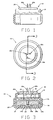
- Fig. 1 is a front elevational view of a condition sensor module made in accordance with the invention, the module provided with a cushioning close ended sleeve member partly broken away;
- Fig. 2 is a top plan view of the Fig. 1 module;
- Fig. 3 is a cross-sectional view of the Fig. 1 module;
- Fig. 4 is a top plan view of an acceleration condition sensing blade member used in the Figs. 1-3 module;
- Fig. 5 is a top plan view of a substrate on which a capacitor detect plate is disposed along with associated electrical traces, the substrate used to mount the acceleration condition sensing blade member of Fig. 4;
- Fig. 6 is a view similar to Fig. 5 showing the acceleration condition sensing blade member mounted on the substrate;
- Fig. 7 is a cross sectional view of Fig. 6 with the addition of a blade member protecting shell received over the blade member and substrate;
- Fig. 7a is a top plan view of a portion of the Fig. 7 shell;
- Fig. 8 is a top plan view of an acceleration condition sensor assembly which comprises first and second modules to detect acceleration forces along two axes extending in different directions;
- Fig. 9 is a right side view of Fig. 8;
- Fig. 10 is a schematic of the Fig. 8 assembly showing interconnection means between the terminals of the modules and the assembly terminals;
- Fig. 11 is a cross sectional view of a modified acceleration condition sensor module mounted on a circuit board;
- Fig. 12 is a cross sectional view of an acceleration condition sensor having a threaded mounting member and having an improved environmental seal;
- Fig. 13 is a top view of the Fig. 12 sensor; and
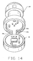
- Fig. 14 is a perspective view of a portion of the Fig. 12 sensor with the electrical connector portion of the sensor partially separated from the substrate to show signal conditioning circuitry of Fig. 12.
-
- Referring to the drawings, a condition-
responsive sensor 10 made in accordance with a first embodiment of the invention and as shown in Figs. 1-7 comprises a generally cylindrical cup-shaped housing 12 formed of suitable material having a bottom 12a and anupstanding wall 12b. Steel is particularly advantageous due to its magnetic shielding characteristics. Asubstrate 18 formed of suitable material such as electrically insulative aluminum oxide, Al2O3, is placed withinhousing 12 preferably on agasket 14 of elastomeric material for a purpose to be described below. It will be understood that the substrate could be composed of various materials such as metal for example, having an electrically insulative top surface or other electrically insulating materials.Substrate 18 is preferably configured as a cylindrical disc conforming generally tohousing 12 and has a bore 18a formed therethrough between opposite face surfaces. An electricallyconductive detect plate 18b (Fig. 5) is provided on atop surface 18c ofsubstrate 18.Plate 18b can be placed on the substrate in any suitable manner as by screen printing.Associated circuit paths surface 18c in a similar manner. Bore 18a is aligned with a sourceplate mounting portion 18f electrically connected topath 18d. A mounting element in the form of apin 22, formed of material having a coefficient of thermal expansion closely matching that ofsubstrate 18, is received in bore 18a. For example, when the substrate employed is composed of 94% alumina ceramic,pin 22 can be formed ofalloy 42, an alloy having a nominal composition by weight of 42% nickel and the balance iron. Bothalloy 42 and 94% alumina have closely matching expansion properties over an appropriate temperature range.Pin 22 is preferably formed with a curved end portion 22a on each end to serve as a weld projection. A recess (not shown) may be formed in the top surface ofsubstrate 18 around bore 18a to enhance flow of coating material fromtrace 18f into the bore. Further details of a suitable pin mounting arrangement can be obtained from application Serial No. 08/148,042 (corresponding to EP 0 652 440, which document falls under Art. 54 (3) EPC.). - An electrically
conductive blade member 24, best seen in Fig. 4, is formed of material having a selected coefficient of thermal expansion relative to that of the substrate and pin to which it is to be mounted, e.g., in the structure described above,alloy 42 would be appropriate.Blade member 24 has a source plate portion 24a, preferably at the center of seismic mass, attached at each lateral side to arespective beam 24b defined by aslot 24c which extends adjacent to the sides essentially the full length ofblade member 24, i.e., along avertical axis 24d from afirst end 24e to a second end 24f of the blade member. Eachslot 24c has aportion 24g which extends generally parallel to thehorizontal axis 24h along the second end of the blade member toward the center of the second end forming a pair or torsion arms 24i each connected to a respectiveelongated beam member 24b at the second end of the blade member.Slot portions 24g have aterminus 24j closely spaced from one another to form a central pivot 24k connecting torsion arms 24i to acentral brace portion 24m.Central brace portion 24m is defined byslots slot 24n forming counter-flexing zones 24o which are connected toattachment portion 24p.Attachment portion 24p is separated from source plate portion 24a by a slot 24t which is in communication withrespective slots 24c.Slots 24t and 24n havecutout portions 24r at opposite sides ofattachment portions 24p to formpivots 24s couplingattachment portions 24p to counter-flex zones 24o. The attachment portion is preferably located at the center of mass to minimize torsional components resulting from forces applied along the horizontal and vertical directions which could adversely affect the connection of the blade member to the pin. Such forces could occur, for example, as a result of dropping the sensor prior to installation. The source plate portion 24a extends frombeam members 24b in a direction back toward the attachment portion. - Although
blade member 24 is similar to that disclosed in copending application Serial No. 08/148,042, mentioned above, the provision of torsion arms 24i and central pivot 24k result in improved sensitivity or deflection of the blade member so that the blade member can be made significantly smaller both in the horizontal and vertical directions while still providing sufficient deflection of the source plate portion in response to acceleration forces along the z axis, i.e., an axis perpendicular to the horizontal and vertical directions. That is, the foot print of the blade member having a given material thickness can be significantly decreased in size and still provide sufficient deflection due to torsion arms 24i and central pivot 24k in spite of the fact that a significant portion of the deflection is provided bybeams 24b extending essentially the full length of the blade and that deflection is proportional to length cubed. As a result, the blade member can be made sufficiently small to fit in a variety of packaging configurations and can be received in locations previously not suitable or not large enough for the larger prior art sensors, as will be discussed in greater detail below. - With particular reference to Fig. 7, a
shell 26 formed of suitable material having a thermal coefficient of expansion close to that ofsubstrate 18, such as a 30% glass filled, liquid crystal polymer when used with the alumina substrate noted above, is preferably received onsubstrate 18.Shell 26 is generally cylindrical having asidewall 26a extending fromend wall 26b. Arecess 26c is formed inend wall 26b to provide space formetal blade member 24 withwall 26b serving to limit deflection of theblade member 24 to prevent overstressing due to abnormally high acceleration forces. Electricallyconductive pins substrate 18, extend through apertures formed inend wall 26b. Raisedareas 26d are formed on the top surface ofshell 26 around thebores receiving pins shell 26 from flowing into the pin bores.Substrate 18 is preferably formed with anindexing notch 18k, see Figs. 5 and 6, which cooperates with anindexing rib 26e formed onsidewall 26a ofshell 26, see Fig. 7a, so thatshell 26 will be properly aligned onsubstrate 18 thereby avoiding any stress from being placed on theconductive pins wall 26a, which also serves to prevent entry of contaminants, extends fromend wall 26b a distance which is slightly less than the thickness ofsubstrate 18. - The substrate and shell assembly of Figure 7 is then received in
housing 12, seen in Fig. 3, onresilient layer 14.Layer 14 is preferably provided with a central open area 14a to prevent the possibility of the material oflayer 14 from extruding into bore 18a when the assembly is fastened tohousing 12 decribed below. Aconnector body 20 having a cavity 20a adapted to receive signal conditioning circuit means 30, such as that shown in coassigned Patent No. 4,875,135 to which reference may be had for further details, is received inhousing 12 overshell 26.Connector body 20mounts terminals housing 12 in any suitable manner, as by bending the outer distal end ofwall 12b inwardly ontoconnector body 20 and against the bias provided byresilient layer 14. - Preferably, a
closed end sleeve 28 of resilient material is placed abouthousing 12 so that if the sensor is subjected to a blow along an axis other than the z axis, e.g., is dropped, the sleeve will cushion the shock and avoid damaging the blade member and/or the mounting of the blade member. -
Sensor 10 can be separately mounted as by clipping it to a bracket or the like. Further, as shown in Figs. 8-10 first and second sensor modules can be mounted in ahousing 42 havingsensor seating cavities 42a, 42b oriented at a selected angle with one another, e.g. 90°, in which arespective sensor 10 can be placed to make a dualaxis sensor assembly 40 so that acceleration forces can be sensed in two different directions. The terminals of each sensor module can be connected through a suitable harness or circuit board toterminals 42c-42f inconnector 42g shown in Fig. 9. For example, the terminals ofsensor module 10 comprising 20b, 20c, 20d are used for power Vcc, output Vo and ground respectively.Terminals 20c (Vcc) and 20d (ground) of onesensor module 10 can be connected torespective terminals second sensor module 10 to reduce the required number of terminals ofdual sensor assembly 40. Preferably the sensors are potted intocavities 42a, 42b and, if desired, alid 44 can be received over the cavities. Suitable mounting holes 42i in mountingbracket 42j can be used to mountsensor assembly 40 to a body whose acceleration is to be monitored using conventional fasteners. Althoughhousing 42 is described having adual sensor assembly 40, it is within the purview of the invention to incorporate three or more sensors oriented at selected angles so that acceleration forces can be sensed in various selected directions, if desired. Fig. 11 shows a modified sensor 10' which usesterminal pins circuit board 50.Substrate 18 is inverted and received on an annular seat 12'c formed in tubular housing 12' with blade member 24', attached to pin 22, disposed betweensubstrate 18 and bottom wall 12'a which serves to prevent over-travel of the blade member. In this embodiment,terminal pins substrate 18 for connection to circuit traces oncircuit board 50. In this embodiment the signal conditioning circuit can be disposed oncircuit board 50, if desired, rather than in the sensor 10' housing. It will be noted that blade member 24' is shown mounted in a non-central location, e.g., atcentral brace portion 24m, although mounting atattachment portion 24p is claimed. - As seen in Fig. 12,
sensor 10" can be mounted by providing a threadedmember 12"d either integrally attached tohousing 12" or attached by welding or the like thereto. A close endedsleeve 12"e of resilient material such as rubber may be placed over threadedmember 12"d prior to use both to protect the thread as well as to provide a cushion along with sleeve 28' in the event thatsensor 10" is dropped on a hard surface. Sleeve 28', in addition to providing a protective cushion, also facilitates mounting of the sensor by providing frictional drive capability. That is, the sensor can be grasped through the sleeve and rotated without having to use thehexagonal mounting portion 12"f. Althoughhousing 12" is shown as being formed of metal, it will be understood that the housing and threaded member could be formed from suitable material, e.g., polymeric material, if desired. - Connector body 20' is shown with a shroud 20'e around terminals 20'b, 20'c, 20'd.
Signal conditioning circuitry 30 received in cavity 20'a is shown comprising a flexible substrate 30a of polyimide or other suitable material on which circuit traces and components are disposed. Atab 30b extends from flexible substrate 30a on which acircuit trace 30d (Fig. 14) is disposed to provide a ground connection forcircuit 30. Conventionally the tab on which the ground trace is disposed extends out of the circuit receiving cavity formed between connector body and the sensor sub-assembly between the connector body and metallic housing member with the distal free end of the housing wall deformed over against the tab and the connector body to make electrical connection between the circuit trace on the tab and the housing member. After deforming the wall of the housing member sealing material such as silicone typically is placed around the interface between the connector body and the housing wall to form an environmental seal in the manner described in U.S. Patent No. 4,875,135 referenced above. However, effective placement of the sealing material is difficult and time consuming and serves as a potential leakage path allowing moisture to penetrate into the circuit cavity if the sealing material is not perfectly placed. As shown in Fig. 12,tab 30b is chosen to have a length only sufficient to extend to a point intermediate the outer distal end ofwall 12b and the bottom of connector body 20'. Adetent 12c is then formed inwall 12b in alignment withtab 30b and extending through the tab into connector body 20' to make an effective electrical connection between the ground trace ontab 30b andhousing 12". A conventional flexible gasket such as 0-ring seal member 13 is then placed around connector body 20' and the outerdistal portion 12d ofhousing 12" is rolled over ontomember 13 to form an effective environmental seal in an easily controlled assembly procedure. Calibration window 20'f can continue to be sealed using conventional epoxy material 20'g, such as silicone rubber, since the opening is sufficiently large that a dispenser can easily and accurately be inserted into it. - It should be understood that although particular embodiments of the invention has been described by way of illustrating the invention, the invention includes all modifications and equivalents thereof falling within the scope of the appended claims.
Claims (15)
- An acceleration condition responsive sensor (10) comprising a substrate (18) having a first surface (18c), an electrically conductive detect plate (18b) mounted on the first surface of the substrate, an electrically conductive blade member (24) having first and second axes in the plane of the blade perpendicular to each other and first (24e) and second (24f) ends and having an attachment portion (24p) which is located generally at the center of mass of the blade member, a source plate portion (24a) and integral resilient beam means extending between the attachment and source plate portions, the resilient beam means including:a pair of elongated beam members (24b) formed by a respective slot (24c) adjacent opposite sides of the blade member and extending in the direction of the first axis essentially from the first end (24e) to the second end (24f) of the blade member, the beam members being connected at the first end of the blade member to the source plate portion (24a), the source plate portion extending back in a direction toward the attachment portion (24p) from the connection with the beam members;a pair of torsion arms (24i) connected to the respective elongated beam members at the second end of the blade member, the respective slots having a portion extending parallel to the second axis along the second end of the blade member toward the center of the second end forming the pair of torsion arms (24i); anda central pivot (24k), the respective slots having a terminus (24j) closely spaced from one another to form the central pivot (24k) ;the blade member (24) being mounted on the substrate (18) via the attachment portion, with the source plate portion (24a) overlying the detect plate (18b) in selected spaced relation, circuit paths being disposed on the substrate electrically connected to the detect plate and the electrically conductive blade member to form a capacitor, the source plate portion being movable relative to the detect plate in response to an acceleration force to provide an electrical signal.
- An acceleration condition responsive sensor according to claim 1, in which the blade member (24) is generally rectangular in a plan view and the substrate is generally cylindrical.
- An acceleration condition responsive sensor according to claim 1, in which the substrate (18) has a bore (18a) extending perpendicular to the first surface, the blade member (24) is attached to a pin (22), the pin being received in the bore.
- An acceleration condition responsive sensor according to claim 1, in which the substrate (18) has a bore (18a) extending perpendicular to the first surface, and the attachment portion (24p) of the blade member (24) is attached to a pin (22), the pin being received in the bore.
- An acceleration condition responsive sensor according to claim 1, further including an over-travel stop spaced a selected distance from the first surface of the substrate to prevent over-travel motion of the blade member.
- An acceleration condition responsive sensor according to claim 5, further including a cup-shaped housing (12) having a bottom wall (12a) and a sidewall (12b) extending from the bottom wall to a distal end portion, a seating shelf formed on the sidewall, the substrate received in the housing with the first surface of the substrate disposed on the seating shelf, the bottom wall (12a) being spaced from the first surface a selected distance to serve as an over-travel stop to prevent over-travel motion of the blade member (24).
- An acceleration condition responsive sensor according to claim 5, further including a cup-shaped housing having a bottom wall and a sidewall extending from the bottom wall to a distal end portion, the substrate being received in the housing with the first surface of the substrate (18) facing away from the bottom wall, a shell (26) having a top wall and a sidewall depending from the top wall, the sidewall of the shell being disposed on the first surface of the substrate with the top wall spaced from the first surface of the substrate a selected distance to serve as an over-travel stop to prevent over-travel motion of the blade member.
- An acceleration condition responsive sensor according to claim 1, further including a metallic cup-shaped housing (12) having a bottom wall and a sidewall extending from the bottom wall to a distal end portion, the substrate (18) being received in the housing with the first surface of the substrate facing away from the bottom wall, a connector body (20) closing the cup-shaped housing and forming a circuit receiving cavity between the connector body and the substrate, a flex circuit substrate received in the cavity, the flex circuit substrate having a tab extending therefrom with a ground circuit trace thereon, the tab extending between the connector body and the sidewall of the housing to a point intermediate the bottom wall of he housing and the distal end portion of the sidewall, a detent formed in the sidewall through the tab and into the connector body to make an electrical connection between the ground circuit trace and the housing, a gasket member received between the connector body and the sidewall of the housing, the distal end portion of the sidewall turned over to capture the gasket member and form an environmental seal.
- An acceleration condition responsive sensor according to claim 8, further including a layer of resilient material (19) disposed between the substrate (18) and the bottom wall of the housing.
- An acceleration condition responsive sensor according to claim 1, further including a cup-shaped housing (12') having a bottom wall and a sidewall extending from the bottom wall to a distal end portion, the substrate received in the housing, the substrate formed with a plurality of pin receiving bores, an electrically conductive terminal pin (18g, 18h, 18i) received in each bore in electrically conductive engagement with circuit paths on the substrate, and a circuit board (50), the electrically conductive terminal pins extending through apertures in the circuit board and being attached to the circuit board to mount the sensor thereon.
- An acceleration condition responsive sensor according to claim 1, further including a cup-shaped housing (12) having a bottom wall and a sidewall extending from the bottom wall, the substrate received in the housing, and resilient material (28) is disposed outside the housing on the side and bottom walls of the housing.
- An acceleration condition responsive sensor according to claim 1, further including a cup-shaped housing (12'') having a bottom wall and a sidewall extending from the bottom wall, the substrate (18) being received in the housing and a threaded member (12''d) extending downwardly from the bottom wall.
- An acceleration condition responsive sensor according to claim 12, in which resilient material (28') is disposed outside the housing on the sidewall.
- An acceleration condition responsive sensor assembly comprising a support, first and second housing sensor seats having a seating surface disposed on the support, the sealing surfaces lying in respective first and second planes which intersect one another, first and second acceleration sensor modules, the first and second sensor modules being mounted in the respective first and second seats with the bottom wall of the respective housing lying in a plane generally parallel with respective first and second planes so that acceleration forces are sensed in two different directions, wherein each of said first and second sensor modules is as claimed in any preceding claim.
- An acceleration condition sensor assembly according to claim 14, in which the first and second planes are perpendicular to one another.
Applications Claiming Priority (2)
| Application Number | Priority Date | Filing Date | Title |
|---|---|---|---|
| US367655 | 1989-06-19 | ||
| US08/367,655 US5542296A (en) | 1995-01-03 | 1995-01-03 | Compact capacitive acceleration sensor |
Publications (3)
| Publication Number | Publication Date |
|---|---|
| EP0721108A2 EP0721108A2 (en) | 1996-07-10 |
| EP0721108A3 EP0721108A3 (en) | 1998-08-05 |
| EP0721108B1 true EP0721108B1 (en) | 2002-10-16 |
Family
ID=23448068
Family Applications (1)
| Application Number | Title | Priority Date | Filing Date |
|---|---|---|---|
| EP95309044A Expired - Lifetime EP0721108B1 (en) | 1995-01-03 | 1995-12-12 | Acceleration condition sensor apparatus |
Country Status (4)
| Country | Link |
|---|---|
| US (1) | US5542296A (en) |
| EP (1) | EP0721108B1 (en) |
| JP (1) | JPH08233856A (en) |
| DE (1) | DE69528572T2 (en) |
Families Citing this family (9)
| Publication number | Priority date | Publication date | Assignee | Title |
|---|---|---|---|---|
| AU1269499A (en) | 1997-10-07 | 1999-04-27 | Electronics Development Corporation | Transducer assembly with smart connector |
| KR20000074442A (en) * | 1999-05-21 | 2000-12-15 | 오세옥 | The Shock Censor for the Various Use |
| EP1162467A3 (en) | 2000-05-30 | 2002-07-24 | Matsushita Electric Industrial Co., Ltd. | Acceleration sensor |
| US7181968B2 (en) * | 2004-08-25 | 2007-02-27 | Autoliv Asp, Inc. | Configurable accelerometer assembly |
| US8186221B2 (en) * | 2009-03-24 | 2012-05-29 | Freescale Semiconductor, Inc. | Vertically integrated MEMS acceleration transducer |
| DE102011005113B4 (en) * | 2011-03-04 | 2026-05-07 | Zf Friedrichshafen Ag | Sensor carrier cover element with an externally accessible recess for a fastening means, housing for a sensor, sensor module and method for assembling a sensor module |
| JP5845672B2 (en) | 2011-07-13 | 2016-01-20 | セイコーエプソン株式会社 | Sensor devices and electronics |
| JP2019035589A (en) | 2017-08-10 | 2019-03-07 | セイコーエプソン株式会社 | Physical quantity sensor, inertia measurement unit, electronic apparatus, and moving object |
| JP6545918B1 (en) * | 2019-05-22 | 2019-07-17 | Imv株式会社 | Acceleration sensor core unit, method for preventing deflection of substrate on which acceleration sensor is mounted |
Family Cites Families (6)
| Publication number | Priority date | Publication date | Assignee | Title |
|---|---|---|---|---|
| US4736629A (en) * | 1985-12-20 | 1988-04-12 | Silicon Designs, Inc. | Micro-miniature accelerometer |
| DE3611360A1 (en) * | 1986-04-04 | 1987-10-08 | Bosch Gmbh Robert | SENSOR FOR AUTOMATIC TRIGGERING OF PASSENGER PROTECTION DEVICES |
| US4875135A (en) * | 1988-12-02 | 1989-10-17 | Texas Instruments Incorporated | Pressure sensor |
| US5239871A (en) * | 1990-12-17 | 1993-08-31 | Texas Instruments Incorporated | Capacitive accelerometer |
| US5345823A (en) * | 1991-11-12 | 1994-09-13 | Texas Instruments Incorporated | Accelerometer |
| US5555766A (en) * | 1993-11-04 | 1996-09-17 | Texas Instruments Incorporated | Acceleration sensor apparatus and method for making same |
-
1995
- 1995-01-03 US US08/367,655 patent/US5542296A/en not_active Expired - Lifetime
- 1995-12-12 DE DE69528572T patent/DE69528572T2/en not_active Expired - Lifetime
- 1995-12-12 EP EP95309044A patent/EP0721108B1/en not_active Expired - Lifetime
- 1995-12-25 JP JP7337235A patent/JPH08233856A/en active Pending
Also Published As
| Publication number | Publication date |
|---|---|
| EP0721108A2 (en) | 1996-07-10 |
| DE69528572T2 (en) | 2003-12-11 |
| EP0721108A3 (en) | 1998-08-05 |
| JPH08233856A (en) | 1996-09-13 |
| DE69528572D1 (en) | 2002-11-21 |
| US5542296A (en) | 1996-08-06 |
Similar Documents
| Publication | Publication Date | Title |
|---|---|---|
| EP0542436B1 (en) | Accelerometer | |
| EP0523862B1 (en) | Accelerometer mounting arrangement having reduced temperature dependance | |
| EP0540071B1 (en) | Accelerometer assembly with evaluation circuit | |
| JP3020426B2 (en) | Transducer assembly, transducer device for mounting to circuit board, and method of mounting transducer to circuit board | |
| EP0660119B1 (en) | Acceleration sensor | |
| US6040625A (en) | Sensor package arrangement | |
| US5548999A (en) | Mounting arrangement for acceleration detector element | |
| US6536287B2 (en) | Simplified capacitance pressure sensor | |
| EP0543430B1 (en) | Pressure sensor and method of assembly thereof | |
| EP0491506B1 (en) | Accelerometer and method of making | |
| EP0519626A1 (en) | Piezoresistive accelerometer with central mass in support | |
| US5542296A (en) | Compact capacitive acceleration sensor | |
| EP1407278B1 (en) | Acceleration sensor | |
| JP3437876B2 (en) | Acceleration sensor device and method of manufacturing the same | |
| EP0550037B1 (en) | Piezoelectric acceleration sensor | |
| US4987780A (en) | Integrated accelerometer assembly | |
| GB2234817A (en) | Integrated accelerometer assembly | |
| JPH07110341A (en) | Three-dimensional acceleration sensor unit and three-dimensional acceleration sensor having the unit packaged | |
| JP2001337107A (en) | Semiconductor acceleration sensor and semiconductor acceleration sensor package |
Legal Events
| Date | Code | Title | Description |
|---|---|---|---|
| PUAI | Public reference made under article 153(3) epc to a published international application that has entered the european phase |
Free format text: ORIGINAL CODE: 0009012 |
|
| AK | Designated contracting states |
Kind code of ref document: A2 Designated state(s): DE FR GB IT NL |
|
| PUAL | Search report despatched |
Free format text: ORIGINAL CODE: 0009013 |
|
| AK | Designated contracting states |
Kind code of ref document: A3 Designated state(s): DE FR GB IT NL |
|
| 17P | Request for examination filed |
Effective date: 19981125 |
|
| 17Q | First examination report despatched |
Effective date: 19991019 |
|
| GRAG | Despatch of communication of intention to grant |
Free format text: ORIGINAL CODE: EPIDOS AGRA |
|
| GRAG | Despatch of communication of intention to grant |
Free format text: ORIGINAL CODE: EPIDOS AGRA |
|
| GRAG | Despatch of communication of intention to grant |
Free format text: ORIGINAL CODE: EPIDOS AGRA |
|
| GRAH | Despatch of communication of intention to grant a patent |
Free format text: ORIGINAL CODE: EPIDOS IGRA |
|
| GRAH | Despatch of communication of intention to grant a patent |
Free format text: ORIGINAL CODE: EPIDOS IGRA |
|
| GRAA | (expected) grant |
Free format text: ORIGINAL CODE: 0009210 |
|
| AK | Designated contracting states |
Kind code of ref document: B1 Designated state(s): DE FR GB IT NL |
|
| PG25 | Lapsed in a contracting state [announced via postgrant information from national office to epo] |
Ref country code: NL Free format text: LAPSE BECAUSE OF FAILURE TO SUBMIT A TRANSLATION OF THE DESCRIPTION OR TO PAY THE FEE WITHIN THE PRESCRIBED TIME-LIMIT Effective date: 20021016 Ref country code: IT Free format text: LAPSE BECAUSE OF FAILURE TO SUBMIT A TRANSLATION OF THE DESCRIPTION OR TO PAY THE FEE WITHIN THE PRE;WARNING: LAPSES OF ITALIAN PATENTS WITH EFFECTIVE DATE BEFORE 2007 MAY HAVE OCCURRED AT ANY TIME BEFORE 2007. THE CORRECT EFFECTIVE DATE MAY BE DIFFERENT FROM THE ONE RECORDED.SCRIBED TIME-LIMIT Effective date: 20021016 |
|
| REG | Reference to a national code |
Ref country code: GB Ref legal event code: FG4D |
|
| REF | Corresponds to: |
Ref document number: 69528572 Country of ref document: DE Date of ref document: 20021121 |
|
| NLV1 | Nl: lapsed or annulled due to failure to fulfill the requirements of art. 29p and 29m of the patents act | ||
| ET | Fr: translation filed | ||
| PLBE | No opposition filed within time limit |
Free format text: ORIGINAL CODE: 0009261 |
|
| STAA | Information on the status of an ep patent application or granted ep patent |
Free format text: STATUS: NO OPPOSITION FILED WITHIN TIME LIMIT |
|
| 26N | No opposition filed |
Effective date: 20030717 |
|
| REG | Reference to a national code |
Ref country code: GB Ref legal event code: 732E |
|
| REG | Reference to a national code |
Ref country code: FR Ref legal event code: TP |
|
| PGFP | Annual fee paid to national office [announced via postgrant information from national office to epo] |
Ref country code: FR Payment date: 20101203 Year of fee payment: 16 |
|
| PGFP | Annual fee paid to national office [announced via postgrant information from national office to epo] |
Ref country code: GB Payment date: 20101123 Year of fee payment: 16 |
|
| PGFP | Annual fee paid to national office [announced via postgrant information from national office to epo] |
Ref country code: DE Payment date: 20101230 Year of fee payment: 16 |
|
| GBPC | Gb: european patent ceased through non-payment of renewal fee |
Effective date: 20111212 |
|
| REG | Reference to a national code |
Ref country code: FR Ref legal event code: ST Effective date: 20120831 |
|
| REG | Reference to a national code |
Ref country code: DE Ref legal event code: R119 Ref document number: 69528572 Country of ref document: DE Effective date: 20120703 |
|
| PG25 | Lapsed in a contracting state [announced via postgrant information from national office to epo] |
Ref country code: DE Free format text: LAPSE BECAUSE OF FAILURE TO SUBMIT A TRANSLATION OF THE DESCRIPTION OR TO PAY THE FEE WITHIN THE PRESCRIBED TIME-LIMIT Effective date: 20120703 Ref country code: GB Free format text: LAPSE BECAUSE OF NON-PAYMENT OF DUE FEES Effective date: 20111212 |
|
| PG25 | Lapsed in a contracting state [announced via postgrant information from national office to epo] |
Ref country code: FR Free format text: LAPSE BECAUSE OF NON-PAYMENT OF DUE FEES Effective date: 20120102 |