EP0720360B1 - An electronic camera with rapid automatic focus of an image upon an image sensor - Google Patents
An electronic camera with rapid automatic focus of an image upon an image sensor Download PDFInfo
- Publication number
- EP0720360B1 EP0720360B1 EP95120382A EP95120382A EP0720360B1 EP 0720360 B1 EP0720360 B1 EP 0720360B1 EP 95120382 A EP95120382 A EP 95120382A EP 95120382 A EP95120382 A EP 95120382A EP 0720360 B1 EP0720360 B1 EP 0720360B1
- Authority
- EP
- European Patent Office
- Prior art keywords
- lines
- image
- sensor
- charge
- electronic camera
- Prior art date
- Legal status (The legal status is an assumption and is not a legal conclusion. Google has not performed a legal analysis and makes no representation as to the accuracy of the status listed.)
- Expired - Lifetime
Links
Images


Classifications
-
- H—ELECTRICITY
- H04—ELECTRIC COMMUNICATION TECHNIQUE
- H04N—PICTORIAL COMMUNICATION, e.g. TELEVISION
- H04N3/00—Scanning details of television systems; Combination thereof with generation of supply voltages
- H04N3/10—Scanning details of television systems; Combination thereof with generation of supply voltages by means not exclusively optical-mechanical
- H04N3/14—Scanning details of television systems; Combination thereof with generation of supply voltages by means not exclusively optical-mechanical by means of electrically scanned solid-state devices
- H04N3/15—Scanning details of television systems; Combination thereof with generation of supply voltages by means not exclusively optical-mechanical by means of electrically scanned solid-state devices for picture signal generation
- H04N3/1575—Picture signal readout register, e.g. shift registers, interline shift registers
-
- H—ELECTRICITY
- H04—ELECTRIC COMMUNICATION TECHNIQUE
- H04N—PICTORIAL COMMUNICATION, e.g. TELEVISION
- H04N23/00—Cameras or camera modules comprising electronic image sensors; Control thereof
- H04N23/60—Control of cameras or camera modules
- H04N23/67—Focus control based on electronic image sensor signals
- H04N23/673—Focus control based on electronic image sensor signals based on contrast or high frequency components of image signals, e.g. hill climbing method
-
- H—ELECTRICITY
- H04—ELECTRIC COMMUNICATION TECHNIQUE
- H04N—PICTORIAL COMMUNICATION, e.g. TELEVISION
- H04N25/00—Circuitry of solid-state image sensors [SSIS]; Control thereof
- H04N25/40—Extracting pixel data from image sensors by controlling scanning circuits, e.g. by modifying the number of pixels sampled or to be sampled
- H04N25/44—Extracting pixel data from image sensors by controlling scanning circuits, e.g. by modifying the number of pixels sampled or to be sampled by partially reading an SSIS array
- H04N25/443—Extracting pixel data from image sensors by controlling scanning circuits, e.g. by modifying the number of pixels sampled or to be sampled by partially reading an SSIS array by reading pixels from selected 2D regions of the array, e.g. for windowing or digital zooming
-
- H—ELECTRICITY
- H04—ELECTRIC COMMUNICATION TECHNIQUE
- H04N—PICTORIAL COMMUNICATION, e.g. TELEVISION
- H04N25/00—Circuitry of solid-state image sensors [SSIS]; Control thereof
- H04N25/70—SSIS architectures; Circuits associated therewith
- H04N25/71—Charge-coupled device [CCD] sensors; Charge-transfer registers specially adapted for CCD sensors
- H04N25/713—Transfer or readout registers; Split readout registers or multiple readout registers
Definitions
- the invention pertains to apparatus for automatically focusing an image upon an electronic image sensor and, more particularly, for rapidly focusing an image upon a progressive scan image sensor based upon signals from a partial area of the sensor.
- An image sensor for an electronic camera ordinarily contains a two-dimensional array of light sensitive photosites.
- an interline transfer sensor the image charge is transferred from the photosites to light-protected vertical registers, through which the image charge is moved to a horizontal readout register.
- a full frame image sensor the image charge is incremented line-by-line through the photosites themselves to a horizontal readout register, from which the image signal is obtained. Since the full frame image sensor does not contain a separate light-protected storage area, a shutter is normally used to block the light and prevent vertical smearing when reading out the image.
- An example of an electronic still camera is the model DCS 200c camera, marketed by Eastman Kodak Company, Rochester, New York.
- This camera uses a high resolution full frame image sensor in an electronic camera back which attaches to a conventional 35mm film camera body.
- the camera body includes a normal focal plane shutter for blocking image light.
- a separate focus sensor is used in the camera body to automatically focus the camera lens. This extra sensor increases the camera cost. It may also result in a less than optimally focused image on the sensor, if the tolerances of the camera lens focusing mechanism, and the tolerances of the focus detector, are not tightly controlled. Therefore, by using the high resolution image sensor itself to focus the camera lens, the camera cost may be reduced, and the camera focusing accuracy may be increased.
- Focusing a camera lens by using the sensor output signal is an iterative process which requires capturing a sequence of images while varying the focus, until a focus-related parameter of the image, such as the "average contrast", is maximized.
- a focus-related parameter of the image such as the "average contrast”
- Prior art camcorders typically use NTSC format interline image sensors, which do not require a mechanical shutter, to perform this type of automatic lens focusing. In these camcorders, the same image that is recorded is also analyzed to provide the focus information. Focusing is done by spatially bandpass filtering a subsection of the video image read out from the sensor. The lens focus position is adjusted to obtain the highest average magnitude output signal (highest average contrast) from the bandpass filter.
- camcorder's image sensor is ordinarily read out at the video field rate (1/60 second) so that the same sensor operating mode is used to provide both the focus information and the final images. In such camcorders, many images may need to be read out before the lens is properly focused. Since the image readout time is relatively rapid (approximately 1/60 second), acceptable focus can typically be achieved in less than a second.
- Focus time can be further improved by application of the technique shown in U.S. Patent No. 5,051,833 (Tsuji).
- This patent describes an electronic still camera in which focus is based on a rectangular subset of the pixels on an interline charge coupled device (CCD) sensor.
- CCD interline charge coupled device
- Tsuji thus describes a focusing mode which takes less time for reading out an image for the purpose of focusing than is taken for reading out an image for normal image capture.
- This focusing mode is employed with an interline transfer sensor, which has light-protected storage areas (vertical registers) and consequently does not require a mechanical shutter. Because the focusing image frames are not usable as captured images, this technique is not useful with camcorders. Moreover, focusing time can remain a problem if rapid utilization of the camera is desired or if longer readout times are required, such as for definitions higher than NTSC resolution.
- Progressive scan image sensors having a noninterlaced architecture such as the Kodak model KAI-0310CM imager, have been developed for high quality color electronic cameras. This sensor has approximately 480 active lines, and approximately 640 active pixels per line.
- a progressive scan sensor provides a higher quality still image than an interlaced sensor, since all lines are captured during the same interval of time. Unlike an interlace sensor, the progressive scan sensor allows the entire image to be read out in a single scan, albeit through light protected vertical registers as in the interline sensor. Mechanical shuttering, therefore, is unnecessary for exposure control (and to prevent vertical smear) as the function can be performed electronically.
- the progressive scan sensor can be read out at slower than video rates without sacrificing performance, since real-time operation is not required. If, however, the image is read out in the same period of time as from an interlaced image sensor, readout timing from a progressive scan image sensor normally requires a clock rate of approximately twice that used with the interlaced image sensor. Such timing would be required, for instance, for an electronic viewfinder or for the rapid acquisition of image data, such as for autofocus determination. For example, an NTSC format interlaced image sensor with 480 lines and 640 pixels per line requires a clock rate of approximately 12 MHz to read out the 640 lines in the 52.4 mSec NTSC standard active line time, which provides a field rate of 1/60 second.
- a progressive scan sensor like the model KAI-310 imager, must read out twice as many lines per field, it must use a clock rate of about 24 mHz to read out all 480 lines in 1/60 second.
- This higher clock rate requires more expensive clock drivers, analog processing, and A/D conversion than interlaced sensors require.
- Such high speed, and thus high cost, components are required for autofocus processing within the focusing area even though, as in Tsuji, the lines above and below the focusing area are not used.
- the advantage of the invention is that the entire focusing sequence occurs rapidly, taking only a fraction of a second. Furthermore, high speed requirements are avoided by dropping lines of image charge within the partial area that is used for autofocus evaluation.
- FIG. 1 A block diagram of a camera using an automatic focus apparatus incorporated into a progressive scan architecture according to the invention is shown in Figure 1.
- the camera includes an optical viewfinder 10 and a user control section 12 having a number of user control buttons, including zoom buttons 14 and a capture button 16.
- zoom buttons 14 and a capture button 16.
- the user turns on the camera (using a power switch (not shown), which may be automatically enabled when the user depresses the zoom buttons 14 or partially depresses the capture button 16).
- the user composes the picture by depressing the "zoom in” or “zoom out” buttons 14, and by adjusting the position of the camera, while observing the viewfinder image.
- the user depresses the capture button 16.
- the camera then captures a single still image, firing a flash 18 if necessary when the ambient illumination level is low.
- the still image is focused upon an image sensor 20 by a motor driven zoom lens 22, which is interconnected with the viewfinder 10 by a mechanical coupling 23.
- the intensity of the image light upon the sensor 20 is regulated by a motor driven mechanical aperture 24 while exposure time is regulated electronically by appropriate clocking of the sensor 20.
- the still image from the image sensor 20 is processed and digitally stored on a removable memory card 26.
- Control of the sensor 20 is provided by a timing and control section 27, which specifically includes a sensor timing circuit 28.
- the sensor timing circuit 28 provides the signals to enable sensor drivers 30, which provides horizontal clocks (H1, H2) and vertical clocks (V1, V2), as well as a signal FDG for activating a drain structure on the sensor 20.
- the output of the image sensor 20 is amplified and processed in an analog gain and sampling (correlated double sampling (CDS)) circuit 32, and converted to digital form in A/D converter 34.
- the A/D output signal is provided to a processor section 35, which includes a digital processor 36 which temporarily stores the still images in a DRAM memory 38.
- the digital processor 36 then perform image processing on the still images, and finally stores the processed images on the removable memory card 26 via a memory card interface circuit 40, which may use the PCMCIA 2.0 standard interface.
- An EPROM memory 42 is used to store the firmware which operates the digital processor 36.
- the motor driven zoom lens 22 includes a zoom motor 44, a focus motor 46, and an aperture motor 48 (all controlled by lens motor drivers 50).
- the timing and control section 27 further includes a control interface 52 connected to the lens motor drivers 50 and to a flash control circuit 55 via a photosystem interface block 54, which controls the operation of the zoom lens 22 and the flash 18.
- the lens zoom position is controlled by the photosystem interface block 54 based on the position input from the zoom control buttons 14.
- the focus is set by the control interface 52 using a focus adjustment signal output by a focus determination circuit 56 within the processor section 35.
- the focus determination circuit 56 processes data from the A/D converter 34 according to a focusing algorithm (which will be described in connection with Figure 8) applied to a selected partial area of the image sensor 20 as the sensor is operated in the focus mode.
- An iterative algorithm in the control interface 52 adjusts the lens focus position, depending on the output of the focus determination circuit 56, until the focus determination process provides a maximum contrast signal.
- the digital processor 36 and the control interface 52 are shown as two separate blocks, in some implementations the same processor could be used to perform both of these functions. Other of the recited functions, such as focus determination, could also be functionally part of one of the processors.
- the sensor 20 is a progressive scan interline image sensor having a noninterlaced architecture, as shown in more detail in Figure 2A.
- the sensor comprises a two-dimensional array of photosites 58, e.g. photodiodes, arranged in rows (lines) and columns, a plurality of vertical registers 59 adjacent photosite columns for transferring rows (lines) of image charge from the photosites 58 to a horizontal register 60 for readout, and a charge drain (specifically, a fast-dump structure 62) interposed between the output of the vertical registers 59 and the horizontal register 60 for eliminating complete rows (lines) of image charge at a time from the image sensor 20 by discharge to a sensor substrate 64.
- photosites 58 e.g. photodiodes
- a preferred image sensor is the Kodak model KAI-0310CM CCD image sensor, which has approximately 480 active lines with approximately 640 active pixels per line and an image aspect ratio of 4:3. This sensor is described in a Performance Specification document available from Eastman Kodak Company, Rochester, New York. Each pixel is 9 microns "square", since both the vertical and horizontal distances between the centers of adjacent pixels are 9 microns.
- the sensor uses a color filter array pattern known as the "Bayer checkerboard" pattern, described in U.S. patent 3,971,065, which is shown in Figure 3.
- Such a color filter array is characterized by a mosaic pattern in which the filter colors alternate in both line and column directions.
- the sensor 20 uses a progressive scan readout method, which allows the entire image to be read out in a single scan. In this operating mode, all of the pixels on the sensor are transferred to the horizontal register 60, which delivers the image signals to the analog gain and CDS circuit 32 (see Figure 1). More specifically, referring to Figure 2A, the accumulated or integrated charge for the photodiodes comprising the photosites 58 is transported from the photosites to light protected vertical (parallel) registers 59 by applying a large positive voltage to the phase-one vertical clock (V1). This reads out every row, or line, into the vertical registers 59. The charge is then transported from the vertical registers 59 to the horizontal register 60 by two-phase clocking of the vertical clocks (V1, V2).
- the fast dump structure 62 Between the vertical and horizontal registers is the fast dump structure 62, which is further described in the Performance Specification document for the KAI-310 sensor.
- FDG fast dump gate line
- charge from the row (line) of pixel values currently adjacent to the fast dump structure 62 is transferred from the CCD channel directly into the sensor substrate 64 rather than to the horizontal register 60.
- This dump, or line clear, is accomplished during the vertical-to-horizontal transfer time.
- the fast dump structure 62 allows lines of charge to be eliminated.
- a conventional use of the gate 62 is to eliminate stray charge in the vertical registers 59 during especially long integration times, and just before transfer of image charge to the vertical registers 59.
- the gate 62 may also be used to eliminate unwanted non-image lines above and below the image.
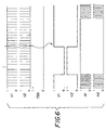
- Figure 4 shows a representative portion of the image sensor 20 which provides the data used to focus the image in the focusing operating mode. Only a small number of lines in a central focusing area 66 of the image are used to provide the focus determination input data.
- the other lines in the outer area 68 are quickly read from the image by continuously holding the fast dump structure 62 at a high positive potential, as the vertical clocks are cycled high and low to transfer lines of charge to the substrate via the fast dump drain. Since the image charge for the non-used lines are quickly flushed from the sensor, this operation is referred to as a "fast flush" and the focus mode is thus described as a fast flush focus mode.
- the time required to read out the image in the fast flush focus mode is well under 10 mSec.
- central focusing area 66 allows even more "images" to be captured per unit time (i.e., more iterative cycles or image "updates"). If more image updates can be obtained in a given period of time, then autofocus can be achieved more rapidly for the same size central focusing area 66 as would be used in the prior art. Alternatively, if the existing update rate is satisfactory, the central focusing area 66 can be enlarged in the vertical direction without decreasing the update rate obtained in the prior art. A larger central focusing area 66 may be useful in focusing on a more appropriate area of the sensor 20.
- the timing and control section 27 operates the electronic camera shown in Figure 1 in two modes, including a first imaging mode wherein all rows of signal charge corresponding to each line are progressively read out through the horizontal register 60 during a single scan, and a second autofocus mode wherein some of the rows of signal charge corresponding to some lines are eliminated through the fast dump structure 62 prior to readout.
- the first mode corresponds to a high quality still imaging mode while the second mode corresponds to a focusing mode for providing central lines of image data to the focus determination circuit 56.
- the timing and control section 27 controls the fast dump structure 62 to A) eliminate all lines of image charge in the outer area 68 ( Figure 4) outside the central focusing area 66, and B) eliminate at least one line of image charge from the image sensor 20 for every one or more lines of image charge that are transferred to the horizontal register 60 for readout from the central focusing area 66.
- the sensor timing circuit 28 is controlled by the control interface 52 to provide the clock signals V1, V2, H1, H2, and the gate signal FDG according to the two modes of operation.
- the timing signals for the first mode are shown in Figure 6; those for the second mode are shown in Figures 7A and 7B.
- the two-phase cycling of signals V1 and V2 control the transfer of lines of image charge from the vertical registers 59 to the horizontal register 60.
- the two-phase cycling of signals H1 and H2 control the transfer of pixels from the horizontal register 60 to subsequent circuits in the camera.
- the level of the signal FDG determines whether the image charge is dumped to the substrate 64 or transferred to the horizontal register 60.
- the sensor 20 includes the aforementioned array of color filters arranged in a particular color pattern (e.g., the checkerboard Bayer pattern of Fig. 3), and the lines of image charge that are transferred to the horizontal register 60 should preserve that particular color pattern in the pattern of lines that are generated, if only for ease of subsequent processing.
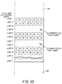
- a pattern of lines in the central focusing area 66 of the sensor 20 is eliminated in the autofocus mode, and the intervening lines are transferred to the horizontal register 60, using the timing shown in Figure 7B.
- the line-skipping pattern for the central focusing area 66 is shown in Figure 10.
- the first two lines (1 and 2) are read out as in the imaging mode. These provide a green-red and a blue-green line.
- the next two lines (3 and 4) are eliminated by turning on the fast dump structure 62 during the time that these lines are transferred past the fast dump structure 62.
- lines 5 and 6 are read out normally, and then lines 7 and 8 are eliminated through the fast dump structure 62.
- This process proceeds through the central area 66 and generates an output image signal having the Bayer-type color filter repeating pattern, so that the signals can be processed using algorithms designed for the Bayer pattern.
- FIG. 7A and 7B shows the clock waveforms for the vertical and horizontal clocks V1, V2, H1, H2 and the fast dump gate FDG for the central focusing area 66.
- another pair of lines i.e., lines 3 and 4, 7 and 8, etc. is eliminated by turning on the fast dump structure 62 during the time that this line pair is transferred past the fast dump structure 62.
- the first line of each saved pair is transferred to the horizontal register 60 and read out according to the timing diagram shown in Figure 7A.
- the second line of each saved pair is transferred to the horizontal register 60, and the succeeding pair of two lines are dumped through the fast dump structure 62, according to the timing diagram shown in Figure 7B.
- the continuation of the sequence of this readout timing achieves readout of the central focusing area 66. This results in a line-skipping sequence of dumping alternate line pairs, and saving intervening line pairs.
- a second embodiment of line skipping in the central area 66 is shown in Figure 11. Basically, six lines are dumped for each two lines that are read out, thus preserving the Bayer-type pattern in the readout signal while gaining further advantage in processing time.
- the area 68 outside the central area 66 continues to be read out by continuously cycling the vertical clocks with the fast dump gate FDG held high.
- the timing is shown in the waveforms of Figures 12A and 12B.
- the first two lines (1 and 2) are read out as in the imaging mode. These provide a green-red and a blue-green line.
- next six lines (3-8) are eliminated by turning on the fast dump structure 62 during the time that these are transferred past the fast dump structure 62--and so on in sequence (save two lines, dump six lines, save two, dump six, etc.) with the remainder of the lines.
- the first line of each saved pair is transferred according to the timing of Figure 12A, and the second line of each saved pair, as well as the six lines that are dumped, are processed according to the timing of Figure 12B.
- the color filter array pattern has been preserved by saving pairs of lines, and then dumping integral numbers of pairs of lines, the pattern may also be preserved by saving single lines and dumping an appropriate number of lines, e.g., save one line and dump seven lines.
- the invention should not be considered limited to a specific color filter array pattern or to any particular line-skipping sequence. Indeed, it is not strictly necessary to preserve the color filter array pattern in order to obtain image data useful for autofocus determination. Nor must lines be dumped in pairs, or in multiples of pairs.
- the advantage of the invention as broadly understood, namely to reduce the amount of data that must be handled from the central focusing area 66, can be obtained by dumping any number or pattern of lines irrespective of the color filter array geometry.
- Figure 8 shows the focus determination circuit.
- This circuit measures the "average contrast" (high frequency detail) of a portion of the image.
- the high frequency detail is obtained by a subtractor 70, which subtracts the value of the current input pixel output by the A/D converter 34 from the value of the A/D output delayed by two pixels, via two registers 72 and 74.
- the two register delay is used instead of a single register, since the horizontal color filter pattern along the line repeats every two pixels. This ensures that similarly colored pixels are subtracted.
- the output of the subtractor is zero when the values of the two pixels are identical.
- the magnitude of the subtractor output increases as the difference between pixel values increases.
- This subtractor output will be large near vertically oriented edges if the camera lens is well focused, but smaller near these same edges if the camera lens is not well focused.
- the absolute value of the subtractor output is combined in a summer 76 with an accumulated value from an accumulator register 78.
- This accumulated value is the average contrast value.
- a single average contrast value may be computed, for example, for the central area 66 shown in Figure 4.
- an accumulator clock input 78a (provided by the control interface processor 52) would be enabled for all pixels in the central area 66 shown in Figure 4, and disabled for any pixels outside this area.
- the accumulated average contrast value is the focus adjustment signal that is used by the control interface 52 and the photosystems interface 54 in the adjustment of the lens 22.
- the circuit in Figure 8 could be modified to include multiple accumulators to store the average contrast for multiple regions in the image.
- the average contrast could be computed for a center region 80, a left central region 82 and the right central region 84 as shown in Figure 5.
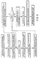
- Figure 9 shows the operating sequence of the camera.
- the user adjusts the zoom setting and points the camera to compose the image, and then presses the still capture button 16.
- the camera focus is adjusted to a mid-range position, and the sensor 20 is cleared of any charge using the fast dump structure 62 for all lines on the entire sensor.
- An image, to be used for focusing the camera lens is then integrated for a period of time, for example 10 mSec, during the focusing mode. During this mode, a top portion of the image is rapidly read out and discarded, using "fast flush" clocking where the vertical and horizontal registers are continuously clocked and the fast dump gate FDG remains high.
- the vertical clock sequence is then set to a line skipping operation (e.g., read two lines, dump two lines, read two, dump two, etc.), while the small number of remaining (not dumped) lines in the central area 66 of the image are clocked out.
- the average absolute value output (average contrast) of a horizontal spatial bandpass filter processing these image lines is used to determine how well the image is focused.
- This average contrast value is stored by the control interface 52, and the lens focus is adjusted while the remainder of the image charge is cleared out using fast flush timing.
- the process of integrating and reading out the focus image is then repeated for a second focusing cycle. If the average contrast increases, the lens focus position is stepped again in the same direction. If the average contrast decreases, the focus position is moved in the opposite direction.
- Figure 2B shows a progressive scan sensor with two readout registers 86 and 88 (which corresponds to the Performance Specification document for the KAI-0310CM image sensor; the preferred embodiment of Figure 2A simply uses but one register).
- the purpose is to double the system speed by having two complete processing channels (analog processing, A/D, etc.); the fast dump structure 62 of such a sensor would be operated as described in connection with foregoing figures to eliminate lines of charge in the central focusing area 66.
- Bayer pattern was described, other mosaic-type filter patterns could be used to advantage, for example, complementary patterns involving cyan, magenta, and yellow filters. While the preferred embodiment maintains the Bayer (mosaic) geometry for the benefit of subsequent algorithms, this is not strictly necessary.
- the line-skipping focusing mode could alternate between saved and dumped lines of charge, with the subsequent processing being accordingly adapted to the particular color progression that is output.
Description
- The invention pertains to apparatus for automatically focusing an image upon an electronic image sensor and, more particularly, for rapidly focusing an image upon a progressive scan image sensor based upon signals from a partial area of the sensor.
- An image sensor for an electronic camera ordinarily contains a two-dimensional array of light sensitive photosites. In an interline transfer sensor, the image charge is transferred from the photosites to light-protected vertical registers, through which the image charge is moved to a horizontal readout register. On the other hand, in a full frame image sensor the image charge is incremented line-by-line through the photosites themselves to a horizontal readout register, from which the image signal is obtained. Since the full frame image sensor does not contain a separate light-protected storage area, a shutter is normally used to block the light and prevent vertical smearing when reading out the image.
- An example of an electronic still camera is the model DCS 200c camera, marketed by Eastman Kodak Company, Rochester, New York. This camera uses a high resolution full frame image sensor in an electronic camera back which attaches to a conventional 35mm film camera body. The camera body includes a normal focal plane shutter for blocking image light. In this type of electronic camera, a separate focus sensor is used in the camera body to automatically focus the camera lens. This extra sensor increases the camera cost. It may also result in a less than optimally focused image on the sensor, if the tolerances of the camera lens focusing mechanism, and the tolerances of the focus detector, are not tightly controlled. Therefore, by using the high resolution image sensor itself to focus the camera lens, the camera cost may be reduced, and the camera focusing accuracy may be increased.
- Focusing a camera lens by using the sensor output signal is an iterative process which requires capturing a sequence of images while varying the focus, until a focus-related parameter of the image, such as the "average contrast", is maximized. Prior art camcorders typically use NTSC format interline image sensors, which do not require a mechanical shutter, to perform this type of automatic lens focusing. In these camcorders, the same image that is recorded is also analyzed to provide the focus information. Focusing is done by spatially bandpass filtering a subsection of the video image read out from the sensor. The lens focus position is adjusted to obtain the highest average magnitude output signal (highest average contrast) from the bandpass filter. Note that the camcorder's image sensor is ordinarily read out at the video field rate (1/60 second) so that the same sensor operating mode is used to provide both the focus information and the final images. In such camcorders, many images may need to be read out before the lens is properly focused. Since the image readout time is relatively rapid (approximately 1/60 second), acceptable focus can typically be achieved in less than a second.
- Focus time can be further improved by application of the technique shown in U.S. Patent No. 5,051,833 (Tsuji). This patent describes an electronic still camera in which focus is based on a rectangular subset of the pixels on an interline charge coupled device (CCD) sensor. During the focusing operation, the image lines within the rectangle are read out at the regular NTSC video rates, while the lines outside the rectangle are read out more rapidly to a charge drain on the CCD sensor. Tsuji thus describes a focusing mode which takes less time for reading out an image for the purpose of focusing than is taken for reading out an image for normal image capture. This focusing mode is employed with an interline transfer sensor, which has light-protected storage areas (vertical registers) and consequently does not require a mechanical shutter. Because the focusing image frames are not usable as captured images, this technique is not useful with camcorders. Moreover, focusing time can remain a problem if rapid utilization of the camera is desired or if longer readout times are required, such as for definitions higher than NTSC resolution.
- A similar system is described in the EP-A-0 421 243 where the charge of the image lines above and below the focusing area are clocked out at high speed in the upward direction and in the downward direction respectively to an overflow drain, and then the signal charges of the image lines comprising the focusing area are transferred at normal clock rate to the horizontal register and then processes for focus determination. This has to be done a plurality of times until the accurate focus point is reached. In this system also timing problems may occur as described above with the Tsuji system since all image lines in the focusing area have to be processed.
- Progressive scan image sensors having a noninterlaced architecture, such as the Kodak model KAI-0310CM imager, have been developed for high quality color electronic cameras. This sensor has approximately 480 active lines, and approximately 640 active pixels per line. A progressive scan sensor provides a higher quality still image than an interlaced sensor, since all lines are captured during the same interval of time. Unlike an interlace sensor, the progressive scan sensor allows the entire image to be read out in a single scan, albeit through light protected vertical registers as in the interline sensor. Mechanical shuttering, therefore, is unnecessary for exposure control (and to prevent vertical smear) as the function can be performed electronically.
- For a high quality still mode, the progressive scan sensor can be read out at slower than video rates without sacrificing performance, since real-time operation is not required. If, however, the image is read out in the same period of time as from an interlaced image sensor, readout timing from a progressive scan image sensor normally requires a clock rate of approximately twice that used with the interlaced image sensor. Such timing would be required, for instance, for an electronic viewfinder or for the rapid acquisition of image data, such as for autofocus determination. For example, an NTSC format interlaced image sensor with 480 lines and 640 pixels per line requires a clock rate of approximately 12 MHz to read out the 640 lines in the 52.4 mSec NTSC standard active line time, which provides a field rate of 1/60 second. Since a progressive scan sensor, like the model KAI-310 imager, must read out twice as many lines per field, it must use a clock rate of about 24 mHz to read out all 480 lines in 1/60 second. This higher clock rate requires more expensive clock drivers, analog processing, and A/D conversion than interlaced sensors require. Such high speed, and thus high cost, components are required for autofocus processing within the focusing area even though, as in Tsuji, the lines above and below the focusing area are not used.
- This leads to the anomalous situation that a non-imaging part of the system, the autofocus processing, requires the higher clock rate, and thus the higher cost parts--clock drivers, analog processing, A/D converters, etc.--than the high resolution imaging part itself. What is needed is a technique for reading out the image sensor data within the focusing area in a manner that decreases the required clock rate while enabling rapid focus of the lens of an electronic camera.
- In arriving at the invention, it was first realized that quick dumping of some parts of the image, even within the focusing area itself, could solve the clocking problem and still leave enough information in the remaining part of the focusing area that the remaining lines of the image could be used for focus evaluation. The problems noted above are then solved according to the invention by basing focus evaluation on a subset of the image lines within the focusing area of the image. This is achieved with an electronic camera according to
claim 1. - Unlike the application of conventional camcorder automatic focusing techniques to interline sensors, which would take several seconds with a progressive scan architecture to bring the lens into focus, the advantage of the invention is that the entire focusing sequence occurs rapidly, taking only a fraction of a second. Furthermore, high speed requirements are avoided by dropping lines of image charge within the partial area that is used for autofocus evaluation.
- The invention will be described in relation to the drawings, wherein
- Figure 1 is a block diagram of an electronic camera incorporating the invention in connection with a progressive scan image sensor;
- Figures 2A and 2B are diagrams of progressive scan image sensors useful with the camera of Figure 1;
- Figure 3 is a diagram of the Bayer color filter geometry for the sensor used with the camera of Figure 1;
- Figure 4 is a diagram of the imaging portion of a sensor showing a central focusing area;
- Figure 5 is a diagram of the imaging portion of a sensor showing a central focusing area divided into regions;
- Figure 6 shows the line timing for the still imaging mode of operation;
- Figures 7A and 7B show the line timing for the autofocus mode of operation;
- Figure 8 is a block diagram of a focus determination circuit used in the camera of Figure 1;
- Figure 9 is a flowchart showing the sequence of operations of the camera of Figure 1;
- Figure 10 shows a first embodiment of a line-skipping pattern, especially for the central focusing area shown in Figure 4;
- Figure 11 shows a second embodiment of a line-skipping pattern for the central focusing area; and
- Figures 12A and 12B shows the line timing for the pattern shown in Figure 11.
-
- A block diagram of a camera using an automatic focus apparatus incorporated into a progressive scan architecture according to the invention is shown in Figure 1. The camera includes an
optical viewfinder 10 and auser control section 12 having a number of user control buttons, includingzoom buttons 14 and acapture button 16. To take a still picture, the user turns on the camera (using a power switch (not shown), which may be automatically enabled when the user depresses thezoom buttons 14 or partially depresses the capture button 16). The user composes the picture by depressing the "zoom in" or "zoom out"buttons 14, and by adjusting the position of the camera, while observing the viewfinder image. When the user is satisfied with the composition, the user depresses thecapture button 16. The camera then captures a single still image, firing aflash 18 if necessary when the ambient illumination level is low. The still image is focused upon animage sensor 20 by a motor drivenzoom lens 22, which is interconnected with theviewfinder 10 by amechanical coupling 23. The intensity of the image light upon thesensor 20 is regulated by a motor drivenmechanical aperture 24 while exposure time is regulated electronically by appropriate clocking of thesensor 20. The still image from theimage sensor 20 is processed and digitally stored on aremovable memory card 26. - Control of the
sensor 20 is provided by a timing andcontrol section 27, which specifically includes asensor timing circuit 28. Thesensor timing circuit 28 provides the signals to enablesensor drivers 30, which provides horizontal clocks (H1, H2) and vertical clocks (V1, V2), as well as a signal FDG for activating a drain structure on thesensor 20. The output of theimage sensor 20 is amplified and processed in an analog gain and sampling (correlated double sampling (CDS))circuit 32, and converted to digital form in A/D converter 34. The A/D output signal is provided to aprocessor section 35, which includes adigital processor 36 which temporarily stores the still images in aDRAM memory 38. Thedigital processor 36 then perform image processing on the still images, and finally stores the processed images on theremovable memory card 26 via a memorycard interface circuit 40, which may use the PCMCIA 2.0 standard interface. AnEPROM memory 42 is used to store the firmware which operates thedigital processor 36. - The motor driven
zoom lens 22 includes azoom motor 44, afocus motor 46, and an aperture motor 48 (all controlled by lens motor drivers 50). The timing andcontrol section 27 further includes acontrol interface 52 connected to thelens motor drivers 50 and to aflash control circuit 55 via aphotosystem interface block 54, which controls the operation of thezoom lens 22 and theflash 18. The lens zoom position is controlled by thephotosystem interface block 54 based on the position input from thezoom control buttons 14. The focus is set by thecontrol interface 52 using a focus adjustment signal output by afocus determination circuit 56 within theprocessor section 35. Thefocus determination circuit 56 processes data from the A/D converter 34 according to a focusing algorithm (which will be described in connection with Figure 8) applied to a selected partial area of theimage sensor 20 as the sensor is operated in the focus mode. An iterative algorithm in thecontrol interface 52 adjusts the lens focus position, depending on the output of thefocus determination circuit 56, until the focus determination process provides a maximum contrast signal. Although thedigital processor 36 and thecontrol interface 52 are shown as two separate blocks, in some implementations the same processor could be used to perform both of these functions. Other of the recited functions, such as focus determination, could also be functionally part of one of the processors. - The
sensor 20 is a progressive scan interline image sensor having a noninterlaced architecture, as shown in more detail in Figure 2A. The sensor comprises a two-dimensional array ofphotosites 58, e.g. photodiodes, arranged in rows (lines) and columns, a plurality ofvertical registers 59 adjacent photosite columns for transferring rows (lines) of image charge from thephotosites 58 to ahorizontal register 60 for readout, and a charge drain (specifically, a fast-dump structure 62) interposed between the output of thevertical registers 59 and thehorizontal register 60 for eliminating complete rows (lines) of image charge at a time from theimage sensor 20 by discharge to asensor substrate 64. A preferred image sensor is the Kodak model KAI-0310CM CCD image sensor, which has approximately 480 active lines with approximately 640 active pixels per line and an image aspect ratio of 4:3. This sensor is described in a Performance Specification document available from Eastman Kodak Company, Rochester, New York. Each pixel is 9 microns "square", since both the vertical and horizontal distances between the centers of adjacent pixels are 9 microns. The sensor uses a color filter array pattern known as the "Bayer checkerboard" pattern, described in U.S. patent 3,971,065, which is shown in Figure 3. Such a color filter array is characterized by a mosaic pattern in which the filter colors alternate in both line and column directions. - The
sensor 20 uses a progressive scan readout method, which allows the entire image to be read out in a single scan. In this operating mode, all of the pixels on the sensor are transferred to thehorizontal register 60, which delivers the image signals to the analog gain and CDS circuit 32 (see Figure 1). More specifically, referring to Figure 2A, the accumulated or integrated charge for the photodiodes comprising thephotosites 58 is transported from the photosites to light protected vertical (parallel) registers 59 by applying a large positive voltage to the phase-one vertical clock (V1). This reads out every row, or line, into the vertical registers 59. The charge is then transported from thevertical registers 59 to thehorizontal register 60 by two-phase clocking of the vertical clocks (V1, V2). Between the vertical and horizontal registers is thefast dump structure 62, which is further described in the Performance Specification document for the KAI-310 sensor. By setting a suitable positive potential on a fast dump gate line FDG, charge from the row (line) of pixel values currently adjacent to thefast dump structure 62 is transferred from the CCD channel directly into thesensor substrate 64 rather than to thehorizontal register 60. This dump, or line clear, is accomplished during the vertical-to-horizontal transfer time. When properly controlled by thesensor timing circuit 28, thefast dump structure 62 allows lines of charge to be eliminated. (A conventional use of thegate 62 is to eliminate stray charge in thevertical registers 59 during especially long integration times, and just before transfer of image charge to the vertical registers 59. Thegate 62 may also be used to eliminate unwanted non-image lines above and below the image.) - Figure 4 shows a representative portion of the
image sensor 20 which provides the data used to focus the image in the focusing operating mode. Only a small number of lines in a central focusingarea 66 of the image are used to provide the focus determination input data. For the progressive scan sensor, the other lines in theouter area 68 are quickly read from the image by continuously holding thefast dump structure 62 at a high positive potential, as the vertical clocks are cycled high and low to transfer lines of charge to the substrate via the fast dump drain. Since the image charge for the non-used lines are quickly flushed from the sensor, this operation is referred to as a "fast flush" and the focus mode is thus described as a fast flush focus mode. The time required to read out the image in the fast flush focus mode is well under 10 mSec. Although it may take 10 iterative cycles for proper focus in some cases, acceptable focus can still be achieved in a fraction of a second. Moreover, as will be described, dropping lines within the central focusingarea 66 allows even more "images" to be captured per unit time (i.e., more iterative cycles or image "updates"). If more image updates can be obtained in a given period of time, then autofocus can be achieved more rapidly for the same size central focusingarea 66 as would be used in the prior art. Alternatively, if the existing update rate is satisfactory, the central focusingarea 66 can be enlarged in the vertical direction without decreasing the update rate obtained in the prior art. A larger central focusingarea 66 may be useful in focusing on a more appropriate area of thesensor 20. - The timing and
control section 27 operates the electronic camera shown in Figure 1 in two modes, including a first imaging mode wherein all rows of signal charge corresponding to each line are progressively read out through thehorizontal register 60 during a single scan, and a second autofocus mode wherein some of the rows of signal charge corresponding to some lines are eliminated through thefast dump structure 62 prior to readout. As applied to the embodiment of Figure 1, the first mode corresponds to a high quality still imaging mode while the second mode corresponds to a focusing mode for providing central lines of image data to thefocus determination circuit 56. In the autofocus mode, the timing andcontrol section 27 controls thefast dump structure 62 to A) eliminate all lines of image charge in the outer area 68 (Figure 4) outside the central focusingarea 66, and B) eliminate at least one line of image charge from theimage sensor 20 for every one or more lines of image charge that are transferred to thehorizontal register 60 for readout from the central focusingarea 66. - The
sensor timing circuit 28 is controlled by thecontrol interface 52 to provide the clock signals V1, V2, H1, H2, and the gate signal FDG according to the two modes of operation. The timing signals for the first mode are shown in Figure 6; those for the second mode are shown in Figures 7A and 7B. The two-phase cycling of signals V1 and V2 control the transfer of lines of image charge from thevertical registers 59 to thehorizontal register 60. The two-phase cycling of signals H1 and H2 control the transfer of pixels from thehorizontal register 60 to subsequent circuits in the camera. The level of the signal FDG determines whether the image charge is dumped to thesubstrate 64 or transferred to thehorizontal register 60. When thesensor 20 is clocked using the first timing mode shown in Figure 6, all lines of the sensor are clocked out, one after the other, through thehorizontal register 60, processed in subsequent camera circuitry, and stored in theremovable memory 26. This timing mode provides a high quality progressive scan still image, but may take 1/30 second or longer to read out the still image. Such timing, however, is acceptable for still mode usage, and, as mentioned before, does not require unusually high speed components. - To provide focusing data to the
focus determination circuit 56, a lower resolution image was found to be suitable. The update rate must be sufficient to provide good focus detection. An update rate of 60 fields/sec is appropriate. Moreover, thesensor 20 includes the aforementioned array of color filters arranged in a particular color pattern (e.g., the checkerboard Bayer pattern of Fig. 3), and the lines of image charge that are transferred to thehorizontal register 60 should preserve that particular color pattern in the pattern of lines that are generated, if only for ease of subsequent processing. To provide this kind of focusing image, a pattern of lines in the central focusingarea 66 of thesensor 20 is eliminated in the autofocus mode, and the intervening lines are transferred to thehorizontal register 60, using the timing shown in Figure 7B. The line-skipping pattern for the central focusingarea 66 is shown in Figure 10. The first two lines (1 and 2) are read out as in the imaging mode. These provide a green-red and a blue-green line. The next two lines (3 and 4) are eliminated by turning on thefast dump structure 62 during the time that these lines are transferred past thefast dump structure 62. Next,lines fast dump structure 62. This process proceeds through thecentral area 66 and generates an output image signal having the Bayer-type color filter repeating pattern, so that the signals can be processed using algorithms designed for the Bayer pattern. More specifically as to waveforms, in thearea 68 surrounding the central focusingarea 66, the vertical clocks are cycled continuously with the fast dump gate FDG held high. This dumps all lines of image charge for theouter area 68 into thesensor substrate 64. Figures 7A and 7B shows the clock waveforms for the vertical and horizontal clocks V1, V2, H1, H2 and the fast dump gate FDG for the central focusingarea 66. For each saved pair of lines (i.e.,lines lines fast dump structure 62 during the time that this line pair is transferred past thefast dump structure 62. The first line of each saved pair is transferred to thehorizontal register 60 and read out according to the timing diagram shown in Figure 7A. The second line of each saved pair is transferred to thehorizontal register 60, and the succeeding pair of two lines are dumped through thefast dump structure 62, according to the timing diagram shown in Figure 7B. The continuation of the sequence of this readout timing achieves readout of the central focusingarea 66. This results in a line-skipping sequence of dumping alternate line pairs, and saving intervening line pairs. - A second embodiment of line skipping in the
central area 66 is shown in Figure 11. Basically, six lines are dumped for each two lines that are read out, thus preserving the Bayer-type pattern in the readout signal while gaining further advantage in processing time. To provide this kind of focusing image, thearea 68 outside thecentral area 66 continues to be read out by continuously cycling the vertical clocks with the fast dump gate FDG held high. Within thecentral area 66, the timing is shown in the waveforms of Figures 12A and 12B. The first two lines (1 and 2) are read out as in the imaging mode. These provide a green-red and a blue-green line. The next six lines (3-8) are eliminated by turning on thefast dump structure 62 during the time that these are transferred past thefast dump structure 62--and so on in sequence (save two lines, dump six lines, save two, dump six, etc.) with the remainder of the lines. As was explained in relation to Figures 7A and 7B, the first line of each saved pair is transferred according to the timing of Figure 12A, and the second line of each saved pair, as well as the six lines that are dumped, are processed according to the timing of Figure 12B. - Although the color filter array pattern has been preserved by saving pairs of lines, and then dumping integral numbers of pairs of lines, the pattern may also be preserved by saving single lines and dumping an appropriate number of lines, e.g., save one line and dump seven lines. Moreover, the invention should not be considered limited to a specific color filter array pattern or to any particular line-skipping sequence. Indeed, it is not strictly necessary to preserve the color filter array pattern in order to obtain image data useful for autofocus determination. Nor must lines be dumped in pairs, or in multiples of pairs. The advantage of the invention as broadly understood, namely to reduce the amount of data that must be handled from the central focusing
area 66, can be obtained by dumping any number or pattern of lines irrespective of the color filter array geometry. - Figure 8 shows the focus determination circuit. This circuit measures the "average contrast" (high frequency detail) of a portion of the image. The high frequency detail is obtained by a
subtractor 70, which subtracts the value of the current input pixel output by the A/D converter 34 from the value of the A/D output delayed by two pixels, via tworegisters summer 76 with an accumulated value from anaccumulator register 78. This accumulated value is the average contrast value. A single average contrast value may be computed, for example, for thecentral area 66 shown in Figure 4. In this instance, anaccumulator clock input 78a (provided by the control interface processor 52) would be enabled for all pixels in thecentral area 66 shown in Figure 4, and disabled for any pixels outside this area. In any event, the accumulated average contrast value is the focus adjustment signal that is used by thecontrol interface 52 and the photosystems interface 54 in the adjustment of thelens 22. Alternately, the circuit in Figure 8 could be modified to include multiple accumulators to store the average contrast for multiple regions in the image. For example, the average contrast could be computed for acenter region 80, a leftcentral region 82 and the rightcentral region 84 as shown in Figure 5. - Figure 9 shows the operating sequence of the camera. The user adjusts the zoom setting and points the camera to compose the image, and then presses the still capture
button 16. The camera focus is adjusted to a mid-range position, and thesensor 20 is cleared of any charge using thefast dump structure 62 for all lines on the entire sensor. An image, to be used for focusing the camera lens, is then integrated for a period of time, for example 10 mSec, during the focusing mode. During this mode, a top portion of the image is rapidly read out and discarded, using "fast flush" clocking where the vertical and horizontal registers are continuously clocked and the fast dump gate FDG remains high. The vertical clock sequence is then set to a line skipping operation (e.g., read two lines, dump two lines, read two, dump two, etc.), while the small number of remaining (not dumped) lines in thecentral area 66 of the image are clocked out. The average absolute value output (average contrast) of a horizontal spatial bandpass filter processing these image lines is used to determine how well the image is focused. This average contrast value is stored by thecontrol interface 52, and the lens focus is adjusted while the remainder of the image charge is cleared out using fast flush timing. The process of integrating and reading out the focus image is then repeated for a second focusing cycle. If the average contrast increases, the lens focus position is stepped again in the same direction. If the average contrast decreases, the focus position is moved in the opposite direction. These focusing cycles are repeated numerous times as the lens focus is adjusted until it provides the maximum average contrast. The entire focusing sequence occurs rapidly, taking only a fraction of a second. Once the average contrast has reached a maximum value, the focus is acceptable. At this point, theentire sensor 20 is cleared, using thefast dump structure 62. The final image is then integrated for a period of time and then transferred to thevertical registers 59, which terminates the exposure. The final image is finally read out from thehorizontal register 60. - The invention has been described with reference to a preferred embodiment. However, it will be appreciated that variations and modifications can be effected by a person of ordinary skill in the art without departing from the scope of the invention. For instance, Figure 2B shows a progressive scan sensor with two
readout registers 86 and 88 (which corresponds to the Performance Specification document for the KAI-0310CM image sensor; the preferred embodiment of Figure 2A simply uses but one register). The purpose is to double the system speed by having two complete processing channels (analog processing, A/D, etc.); thefast dump structure 62 of such a sensor would be operated as described in connection with foregoing figures to eliminate lines of charge in the central focusingarea 66. Furthermore, although the Bayer pattern was described, other mosaic-type filter patterns could be used to advantage, for example, complementary patterns involving cyan, magenta, and yellow filters. While the preferred embodiment maintains the Bayer (mosaic) geometry for the benefit of subsequent algorithms, this is not strictly necessary. The line-skipping focusing mode could alternate between saved and dumped lines of charge, with the subsequent processing being accordingly adapted to the particular color progression that is output.
Claims (10)
- An electronic camera having an automatically focused lens (22) that is operable to focus an image based on image data electronically obtained by the camera from a partial area (66) of the whole image, the camera further having a progressive scan image sensor (20) comprising a two-dimensional array of photosites (58) arranged in lines and columns to provide image charge, the sensor having the capacity to eliminate some lines of image charge and to transfer other lines of image charge, and a timing and control section (27) for controlling the sensor (20) to noninterlaced read out of complete image frames from the sensor, characterized bya charge drain (62) being controlled in a focus mode by said timing and control section (27) so as to eliminate a pattern of lines of image charge from the partial area (66) and to transfer the intervening lines of image charge within the partial area; anda processor (35) for generating a focus adjustment signal based on the intervening lines of image charge transferred from the partial area (66).
- An electronic camera as claimed in claim 1 wherein the timing and control section (27) controls the image sensor (20) so as to eliminate all lines of image charge from the remaining area outside the partial area (66).
- An electronic camera as claimed in claim 1 wherein the timing and control section (27) generates a pattern of eliminated lines within the partial area (66) by eliminating two or more consecutive lines of image charge within the partial area for every two lines of image charge that are transferred from the partial area.
- An electronic camera as claimed in claim 3 wherein two lines are eliminated for every two lines that are transferred.
- An electronic camera as claimed in claim 3 wherein six lines are eliminated for every two lines that are transferred.
- An electronic camera as claimed in claim 1 wherein the partial area (66) is a central area of the whole image.
- An electronic camera as claimed in claim 1 wherein said image sensor (20) comprises a plurality of vertical registers (59) adjacent photosite columns for transferring lines of image charge from the photosites to a horizontal register (60) for readout as image data;said charge drain (62) being interposed between the output of the vertical registers (59) and the horizontal register (60) for eliminating complete lines of image charge at a time from the image sensor; andsaid timing and control section (27) controlling the charge drain (62) so as to eliminate at least one line of image charge from the central area (66) of the image sensor (20) for every one or more consecutive lines of image charge that is transferred from the central area to the horizontal register (60) for readout, thereby generating a pattern of transferred lines suitable for focus determination.
- An electronic camera as claimed in claim 7 wherein said timing and control section (27) provides a pattern of lines within the central area (66) by eliminating two or more consecutive lines of image charge for every two lines of image charge that are transferred to the horizontal register (60).
- An electronic camera as claimed in claim 8 wherein two lines are eliminated for every two lines that are transferred.
- An electronic camera as claimed in claim 7 wherein the image sensor (20) is a color sensor having an array of color filters arranged in a particular color pattern and wherein the lines of image charge that are transferred to the horizontal register preserve the particular color pattern in the pattern of lines that are generated for readout.
Applications Claiming Priority (2)
| Application Number | Priority Date | Filing Date | Title |
|---|---|---|---|
| US08/367,404 US5668597A (en) | 1994-12-30 | 1994-12-30 | Electronic camera with rapid automatic focus of an image upon a progressive scan image sensor |
| US367404 | 1994-12-30 |
Publications (2)
| Publication Number | Publication Date |
|---|---|
| EP0720360A1 EP0720360A1 (en) | 1996-07-03 |
| EP0720360B1 true EP0720360B1 (en) | 2000-03-22 |
Family
ID=23447032
Family Applications (1)
| Application Number | Title | Priority Date | Filing Date |
|---|---|---|---|
| EP95120382A Expired - Lifetime EP0720360B1 (en) | 1994-12-30 | 1995-12-22 | An electronic camera with rapid automatic focus of an image upon an image sensor |
Country Status (4)
| Country | Link |
|---|---|
| US (1) | US5668597A (en) |
| EP (1) | EP0720360B1 (en) |
| JP (1) | JP3234473B2 (en) |
| DE (1) | DE69515833T2 (en) |
Families Citing this family (138)
| Publication number | Priority date | Publication date | Assignee | Title |
|---|---|---|---|---|
| US6860428B1 (en) * | 1998-09-11 | 2005-03-01 | Robotic Vision Systems Inc. | Optical symbologies imager |
| JP3351667B2 (en) * | 1995-10-02 | 2002-12-03 | ペンタックス株式会社 | Monitor display device and color filter |
| US6147707A (en) * | 1996-02-06 | 2000-11-14 | Canon Kabushiki Kaisha | Method and apparatus for gain adjustment of an image sensor |
| JPH10136244A (en) * | 1996-11-01 | 1998-05-22 | Olympus Optical Co Ltd | Electronic image pickup device |
| JPH10170813A (en) | 1996-12-11 | 1998-06-26 | Canon Inc | Focus detector, automatic focusing device, and camera |
| JP3907778B2 (en) * | 1997-04-08 | 2007-04-18 | オリンパス株式会社 | Imaging system |
| US6847401B1 (en) * | 1997-08-25 | 2005-01-25 | Sanyo Electric Co., Ltd. | Solid-state image pickup device for producing thinned image |
| JP3977906B2 (en) * | 1997-09-26 | 2007-09-19 | オリンパス株式会社 | Automatic focus adjustment device |
| JPH11112883A (en) * | 1997-09-30 | 1999-04-23 | Olympus Optical Co Ltd | Image pickup device |
| JPH11112882A (en) * | 1997-09-30 | 1999-04-23 | Olympus Optical Co Ltd | Image pickup device |
| JP4019235B2 (en) * | 1998-06-05 | 2007-12-12 | 富士フイルム株式会社 | Imaging device driving method and electronic camera |
| US6906751B1 (en) * | 1998-07-22 | 2005-06-14 | Minolta Co., Ltd. | Digital camera and control method thereof |
| JP4160664B2 (en) * | 1998-08-04 | 2008-10-01 | 株式会社リコー | Autofocus device, camera, and in-focus position determination method |
| WO2000019710A1 (en) * | 1998-09-25 | 2000-04-06 | Unisearch Limited | Ccd readout method |
| US6580457B1 (en) | 1998-11-03 | 2003-06-17 | Eastman Kodak Company | Digital camera incorporating high frame rate mode |
| JP3932006B2 (en) * | 1998-12-02 | 2007-06-20 | 株式会社日立製作所 | Imaging device |
| JP3943273B2 (en) * | 1999-01-28 | 2007-07-11 | 富士フイルム株式会社 | Solid-state imaging device and signal readout method |
| US6809764B1 (en) * | 1999-05-12 | 2004-10-26 | Fuji Photo Film Co., Ltd. | Solid-state electronic image sensing device with high subsampling efficiency and method of reading a video signal out of the same |
| EP1188309B1 (en) * | 1999-05-21 | 2003-08-20 | Foveon, Inc. | Targetable autofocus system |
| US6252627B1 (en) * | 1999-08-25 | 2001-06-26 | Ball Aerospace & Technologies Corp. | Star tracker detector having a partial memory section |
| JP4022682B2 (en) * | 1999-09-14 | 2007-12-19 | 富士フイルム株式会社 | Imaging apparatus and image output method |
| US6522889B1 (en) * | 1999-12-23 | 2003-02-18 | Nokia Corporation | Method and apparatus for providing precise location information through a communications network |
| JP3991543B2 (en) * | 2000-01-11 | 2007-10-17 | 株式会社日立製作所 | Imaging device |
| JP4277404B2 (en) * | 2000-01-25 | 2009-06-10 | ソニー株式会社 | Image shooting device |
| US6693671B1 (en) | 2000-03-22 | 2004-02-17 | Eastman Kodak Company | Fast-dump structure for full-frame image sensors with lod antiblooming structures |
| US6507056B1 (en) | 2000-03-22 | 2003-01-14 | Eastman Kodak Company | Fast line dump structure for solid state image sensor |
| US6785414B1 (en) | 2000-09-28 | 2004-08-31 | Media Cybernetics, Inc. | System and method for establishing an aggregate degree of brightness for each primary color to create a composite color digital image |
| JP4341177B2 (en) * | 2000-12-15 | 2009-10-07 | ソニー株式会社 | Solid-state imaging device, driving method thereof, and image reading device |
| US20020097330A1 (en) * | 2001-01-25 | 2002-07-25 | Spears Kurt E. | Photosensor array using segmented charge transfer gates to improve processing time for small images |
| US6837431B2 (en) * | 2002-04-09 | 2005-01-04 | Symbol Technologies, Inc. | Semiconductor device adapted for imaging bar code symbols |
| JP3797543B2 (en) * | 2001-10-26 | 2006-07-19 | 富士写真フイルム株式会社 | Automatic focus adjustment device |
| US7053953B2 (en) * | 2001-12-21 | 2006-05-30 | Eastman Kodak Company | Method and camera system for blurring portions of a verification image to show out of focus areas in a captured archival image |
| JP2003244495A (en) * | 2002-02-14 | 2003-08-29 | Canon Inc | Housing apparatus |
| JP3967165B2 (en) * | 2002-03-27 | 2007-08-29 | 富士フイルム株式会社 | Digital still camera |
| US20030193600A1 (en) * | 2002-03-28 | 2003-10-16 | Minolta Co., Ltd | Image capturing apparatus |
| US20050073729A1 (en) * | 2002-06-06 | 2005-04-07 | Urs Schmid | Process and system for evaluating an optical recording |
| DE10226274B4 (en) * | 2002-06-06 | 2006-07-06 | Leica Microsystems (Schweiz) Ag | Method and system for evaluating an optical image |
| JP3986988B2 (en) * | 2002-09-27 | 2007-10-03 | 富士フイルム株式会社 | Automatic focusing method and apparatus |
| US6747808B2 (en) * | 2002-10-04 | 2004-06-08 | Hewlett-Packard Development Company, L.P. | Electronic imaging device focusing |
| US7561793B2 (en) * | 2002-11-12 | 2009-07-14 | Eastman Kodak Company | User interface for controlling cropping in electronic camera |
| US7006764B2 (en) * | 2002-11-12 | 2006-02-28 | Eastman Kodak Company | User interface for controlling cropping in electronic camera |
| US6907194B2 (en) | 2002-11-12 | 2005-06-14 | Eastman Kodak Company | Camera having continuously cropping viewfinder |
| US7046924B2 (en) * | 2002-11-25 | 2006-05-16 | Eastman Kodak Company | Method and computer program product for determining an area of importance in an image using eye monitoring information |
| US7423679B2 (en) * | 2002-12-20 | 2008-09-09 | Eastman Kodak Company | Imaging system having extended useful latitude |
| US7327890B2 (en) * | 2002-12-20 | 2008-02-05 | Eastman Kodak Company | Imaging method and system for determining an area of importance in an archival image |
| US20040123131A1 (en) * | 2002-12-20 | 2004-06-24 | Eastman Kodak Company | Image metadata processing system and method |
| US7301562B2 (en) * | 2003-02-06 | 2007-11-27 | Eastman Kodak Company | Imaging system with delayed verification image presentation |
| US20040155977A1 (en) * | 2003-02-07 | 2004-08-12 | Clark Airell R. | Digital camera that enters a sub-sampling mode for at least one auto function |
| US8218052B2 (en) * | 2003-03-07 | 2012-07-10 | Iconix Video, Inc. | High frame rate high definition imaging system and method |
| US6801719B1 (en) * | 2003-03-14 | 2004-10-05 | Eastman Kodak Company | Camera using beam splitter with micro-lens image amplification |
| US8125695B2 (en) * | 2003-03-24 | 2012-02-28 | Hewlett-Packard Development Company, L.P. | Imaging system and method |
| US7310477B2 (en) * | 2003-08-26 | 2007-12-18 | Eastman Kodak Company | Photographic film cartridge or cassette systems with microlens |
| US7379106B2 (en) * | 2003-08-27 | 2008-05-27 | Hewlett-Packard Development Company, L.P. | Methods and apparatus for reading a CCD architecture in a sampling mode and a non-sampling mode |
| US8462244B2 (en) * | 2003-08-27 | 2013-06-11 | Hewlett-Packard Development Company, L.P. | Adaptively reading one or more but fewer than all pixels of image sensor |
| JP4416462B2 (en) * | 2003-09-19 | 2010-02-17 | パナソニック株式会社 | Autofocus method and autofocus camera |
| WO2005046248A1 (en) * | 2003-11-11 | 2005-05-19 | Olympus Corporation | Multi-spectrum image pick up device |
| US7705908B2 (en) * | 2003-12-16 | 2010-04-27 | Eastman Kodak Company | Imaging method and system for determining camera operating parameter |
| US20050134719A1 (en) * | 2003-12-23 | 2005-06-23 | Eastman Kodak Company | Display device with automatic area of importance display |
| US8659619B2 (en) | 2004-03-26 | 2014-02-25 | Intellectual Ventures Fund 83 Llc | Display device and method for determining an area of importance in an original image |
| US7385638B2 (en) * | 2004-04-28 | 2008-06-10 | Eastman Kodak Company | Image sensor for still or video photography |
| US20050248676A1 (en) * | 2004-05-08 | 2005-11-10 | Mark Christenson | High-speed frame transfer of sub-frame area |
| US20050280726A1 (en) * | 2004-06-18 | 2005-12-22 | Eastman Kodak Company | Image sensor for still or video photography |
| JP4732748B2 (en) * | 2004-07-02 | 2011-07-27 | ソニー株式会社 | Electronic camera and autofocus method |
| US20060044441A1 (en) * | 2004-08-27 | 2006-03-02 | Eastman Kodak Company | Image sensor for still or video photography |
| US20060044399A1 (en) * | 2004-09-01 | 2006-03-02 | Eastman Kodak Company | Control system for an image capture device |
| US20060082670A1 (en) * | 2004-10-14 | 2006-04-20 | Eastman Kodak Company | Interline CCD for still and video photography with extended dynamic range |
| US20060125928A1 (en) * | 2004-12-10 | 2006-06-15 | Eastman Kodak Company | Scene and user image capture device and method |
| US7379107B2 (en) * | 2004-12-10 | 2008-05-27 | Eastman Kodak Company | Image sensor for still or video photography |
| US7236306B2 (en) * | 2005-02-18 | 2007-06-26 | Eastman Kodak Company | Digital camera using an express zooming mode to provide expedited operation over an extended zoom range |
| US7561191B2 (en) * | 2005-02-18 | 2009-07-14 | Eastman Kodak Company | Camera phone using multiple lenses and image sensors to provide an extended zoom range |
| US20060187322A1 (en) * | 2005-02-18 | 2006-08-24 | Janson Wilbert F Jr | Digital camera using multiple fixed focal length lenses and multiple image sensors to provide an extended zoom range |
| US7206136B2 (en) * | 2005-02-18 | 2007-04-17 | Eastman Kodak Company | Digital camera using multiple lenses and image sensors to provide an extended zoom range |
| US7256944B2 (en) * | 2005-02-18 | 2007-08-14 | Eastman Kodak Company | Compact image capture assembly using multiple lenses and image sensors to provide an extended zoom range |
| JP4630200B2 (en) * | 2005-03-07 | 2011-02-09 | 富士フイルム株式会社 | Solid-state imaging device and imaging apparatus |
| KR100706953B1 (en) | 2005-07-11 | 2007-04-12 | 삼성전기주식회사 | Auto focusing apparatus of camera and method of auto focusing |
| JP4797522B2 (en) * | 2005-09-08 | 2011-10-19 | カシオ計算機株式会社 | Imaging apparatus and program thereof |
| US20070070231A1 (en) * | 2005-09-23 | 2007-03-29 | Fujifilm Electronic Imaging Ltd. | Radiation monitoring apparatus and method |
| CN101326814A (en) * | 2005-11-15 | 2008-12-17 | 诺基亚公司 | Imaging system with adjustable optical device |
| US7636119B2 (en) * | 2005-12-21 | 2009-12-22 | Eastman Kodak Company | Image sensor for still or video photography |
| JP2008015097A (en) | 2006-07-04 | 2008-01-24 | Samsung Techwin Co Ltd | Imaging device and imaging method |
| US20080030592A1 (en) * | 2006-08-01 | 2008-02-07 | Eastman Kodak Company | Producing digital image with different resolution portions |
| US7859588B2 (en) | 2007-03-09 | 2010-12-28 | Eastman Kodak Company | Method and apparatus for operating a dual lens camera to augment an image |
| US7729602B2 (en) * | 2007-03-09 | 2010-06-01 | Eastman Kodak Company | Camera using multiple lenses and image sensors operable in a default imaging mode |
| US7676146B2 (en) * | 2007-03-09 | 2010-03-09 | Eastman Kodak Company | Camera using multiple lenses and image sensors to provide improved focusing capability |
| US7683962B2 (en) * | 2007-03-09 | 2010-03-23 | Eastman Kodak Company | Camera using multiple lenses and image sensors in a rangefinder configuration to provide a range map |
| US7576307B2 (en) * | 2007-04-30 | 2009-08-18 | General Electric Company | Microscope with dual image sensors for rapid autofocusing |
| US8957981B2 (en) | 2010-03-03 | 2015-02-17 | Intellectual Ventures Fund 83 Llc | Imaging device for capturing self-portrait images |
| US20110228074A1 (en) * | 2010-03-22 | 2011-09-22 | Parulski Kenneth A | Underwater camera with presssure sensor |
| US20110228075A1 (en) | 2010-03-22 | 2011-09-22 | Madden Thomas E | Digital camera with underwater capture mode |
| JP5403369B2 (en) | 2010-03-31 | 2014-01-29 | ソニー株式会社 | Solid-state imaging device, driving method, and electronic apparatus |
| US8665340B2 (en) | 2010-04-29 | 2014-03-04 | Intellectual Ventures Fund 83 Llc | Indoor/outdoor scene detection using GPS |
| US8605221B2 (en) | 2010-05-25 | 2013-12-10 | Intellectual Ventures Fund 83 Llc | Determining key video snippets using selection criteria to form a video summary |
| US8446490B2 (en) | 2010-05-25 | 2013-05-21 | Intellectual Ventures Fund 83 Llc | Video capture system producing a video summary |
| US8432965B2 (en) | 2010-05-25 | 2013-04-30 | Intellectual Ventures Fund 83 Llc | Efficient method for assembling key video snippets to form a video summary |
| US8599316B2 (en) | 2010-05-25 | 2013-12-03 | Intellectual Ventures Fund 83 Llc | Method for determining key video frames |
| US8619150B2 (en) | 2010-05-25 | 2013-12-31 | Intellectual Ventures Fund 83 Llc | Ranking key video frames using camera fixation |
| US8520088B2 (en) | 2010-05-25 | 2013-08-27 | Intellectual Ventures Fund 83 Llc | Storing a video summary as metadata |
| US8432456B2 (en) | 2010-06-18 | 2013-04-30 | Apple Inc. | Digital camera for sharing digital images |
| US20120019704A1 (en) | 2010-07-26 | 2012-01-26 | Levey Charles I | Automatic digital camera photography mode selection |
| US8970720B2 (en) | 2010-07-26 | 2015-03-03 | Apple Inc. | Automatic digital camera photography mode selection |
| US20120050570A1 (en) | 2010-08-26 | 2012-03-01 | Jasinski David W | Audio processing based on scene type |
| EP4007270A1 (en) | 2010-09-13 | 2022-06-01 | Contour IP Holding, LLC | Portable digital video camera configured for remote image acquisition control and viewing |
| US8494301B2 (en) | 2010-09-16 | 2013-07-23 | Eastman Kodak Company | Refocusing images using scene captured images |
| US20120113515A1 (en) | 2010-11-10 | 2012-05-10 | Karn Keith S | Imaging system with automatically engaging image stabilization |
| US8643734B2 (en) | 2010-11-10 | 2014-02-04 | Apple Inc. | Automatic engagement of image stabilization |
| US9013602B2 (en) | 2011-01-03 | 2015-04-21 | Intellectual Ventures Fund 83 Llc | Digital camera system having a retail mode |
| US8224176B1 (en) | 2011-01-10 | 2012-07-17 | Eastman Kodak Company | Combined ambient and flash exposure for improved image quality |
| US8428308B2 (en) | 2011-02-04 | 2013-04-23 | Apple Inc. | Estimating subject motion for capture setting determination |
| US8379934B2 (en) | 2011-02-04 | 2013-02-19 | Eastman Kodak Company | Estimating subject motion between image frames |
| US20120236173A1 (en) | 2011-03-17 | 2012-09-20 | Telek Michael J | Digital camera user interface which adapts to environmental conditions |
| US8736704B2 (en) | 2011-03-25 | 2014-05-27 | Apple Inc. | Digital camera for capturing an image sequence |
| US20120243802A1 (en) | 2011-03-25 | 2012-09-27 | William Vernon Fintel | Composite image formed from an image sequence |
| US8736697B2 (en) | 2011-03-25 | 2014-05-27 | Apple Inc. | Digital camera having burst image capture mode |
| US20120249853A1 (en) | 2011-03-28 | 2012-10-04 | Marc Krolczyk | Digital camera for reviewing related images |
| US8736716B2 (en) | 2011-04-06 | 2014-05-27 | Apple Inc. | Digital camera having variable duration burst mode |
| US9241101B2 (en) | 2011-05-04 | 2016-01-19 | Intellectual Ventures Fund 83 Llc | Digital camera user interface for text entry |
| US9848158B2 (en) | 2011-05-04 | 2017-12-19 | Monument Peak Ventures, Llc | Digital camera user interface for video trimming |
| US8780180B2 (en) | 2011-05-13 | 2014-07-15 | Apple Inc. | Stereoscopic camera using anaglyphic display during capture |
| US8643746B2 (en) | 2011-05-18 | 2014-02-04 | Intellectual Ventures Fund 83 Llc | Video summary including a particular person |
| US8665345B2 (en) | 2011-05-18 | 2014-03-04 | Intellectual Ventures Fund 83 Llc | Video summary including a feature of interest |
| US8754953B2 (en) | 2011-06-24 | 2014-06-17 | Apple Inc. | Digital camera providing an extended focus range |
| WO2012177495A1 (en) | 2011-06-24 | 2012-12-27 | Eastman Kodak Company | Digital camera providing an extended focus range |
| US8760527B2 (en) | 2011-06-24 | 2014-06-24 | Apple Inc. | Extending a digital camera focus range |
| US9055276B2 (en) | 2011-07-29 | 2015-06-09 | Apple Inc. | Camera having processing customized for identified persons |
| DE102011123037B3 (en) | 2011-09-05 | 2019-10-10 | Carl Zeiss Ag | Method of capturing images of an observation object with an electronic image sensor and optical observation device |
| US20130064531A1 (en) | 2011-09-13 | 2013-03-14 | Bruce Harold Pillman | Zoom flash with no moving parts |
| WO2013043488A1 (en) | 2011-09-22 | 2013-03-28 | Eastman Kodak Company | Digital imaging system with refocusable imaging mode |
| US8593564B2 (en) | 2011-09-22 | 2013-11-26 | Apple Inc. | Digital camera including refocusable imaging mode adaptor |
| US8750674B2 (en) | 2011-09-26 | 2014-06-10 | Intellectual Ventures Fund 83 Llc | Remotely controllable digital video camera system |
| US9253340B2 (en) | 2011-11-11 | 2016-02-02 | Intellectual Ventures Fund 83 Llc | Wireless camera with image sharing prioritization |
| US20130177242A1 (en) | 2012-01-10 | 2013-07-11 | James E. Adams, Jr. | Super-resolution image using selected edge pixels |
| US8866943B2 (en) | 2012-03-09 | 2014-10-21 | Apple Inc. | Video camera providing a composite video sequence |
| US8934045B2 (en) | 2012-03-12 | 2015-01-13 | Apple Inc. | Digital camera system having remote control |
| US20130235234A1 (en) | 2012-03-12 | 2013-09-12 | Megan Lyn Cucci | Digital camera having multiple image capture systems |
| US8928772B2 (en) | 2012-09-21 | 2015-01-06 | Eastman Kodak Company | Controlling the sharpness of a digital image |
| US8724919B2 (en) | 2012-09-21 | 2014-05-13 | Eastman Kodak Company | Adjusting the sharpness of a digital image |
| JP2017526507A (en) | 2014-08-31 | 2017-09-14 | ベレシュトカ,ジョン | System and method for analyzing eyes |
| GB201610434D0 (en) * | 2016-06-15 | 2016-07-27 | Q-Linea Ab | Image based analysis of samples |
Family Cites Families (20)
| Publication number | Priority date | Publication date | Assignee | Title |
|---|---|---|---|---|
| US4047187A (en) * | 1974-04-01 | 1977-09-06 | Canon Kabushiki Kaisha | System for exposure measurement and/or focus detection by means of image senser |
| US3971065A (en) * | 1975-03-05 | 1976-07-20 | Eastman Kodak Company | Color imaging array |
| JPH028456Y2 (en) * | 1984-10-26 | 1990-02-28 | ||
| JPH0773347B2 (en) * | 1985-10-18 | 1995-08-02 | 日本電気株式会社 | Driving method for solid-state imaging device |
| US4752831A (en) * | 1986-05-20 | 1988-06-21 | Polaroid Corporation | Focusing system for camera apparatus |
| US4974092A (en) * | 1988-05-17 | 1990-11-27 | Fuji Photo Film Co., Ltd. | Automatic focusing device for a camera adopting linear sampling of a video signal |
| JPH0748828B2 (en) * | 1988-06-01 | 1995-05-24 | 日本電気株式会社 | Solid-state image sensor |
| US4876608A (en) * | 1988-11-07 | 1989-10-24 | Xerox Corporation | Focus and signal to noise measurement routines in input scanners |
| US5051833A (en) * | 1989-04-28 | 1991-09-24 | Casio Computer Co., Ltd. | Camera apparatus capable of freely setting objective area within viewed subject |
| JP2728943B2 (en) * | 1989-07-08 | 1998-03-18 | キヤノン株式会社 | Lens control device |
| JPH03117275A (en) * | 1989-09-29 | 1991-05-20 | Sanyo Electric Co Ltd | Automatic focus camera |
| US5196939A (en) * | 1989-12-28 | 1993-03-23 | Loral Fairchild Corporation | Method and apparatus for transferring images from an imaging array |
| JPH0418872A (en) * | 1990-05-11 | 1992-01-23 | Nippon Philips Kk | Automatic focusing controller |
| US5233431A (en) * | 1990-10-26 | 1993-08-03 | Fuji Photo Film Co., Ltd. | Image pickup device |
| US5347371A (en) * | 1990-11-29 | 1994-09-13 | Hitachi, Ltd. | Video camera with extraction unit for extracting specific portion of video signal |
| JP2935901B2 (en) * | 1990-12-06 | 1999-08-16 | キヤノン株式会社 | Imaging device |
| US5394187A (en) * | 1992-06-26 | 1995-02-28 | Apollo Camera, L.L.C. | Video imaging systems and method using a single interline progressive scanning sensor and sequential color object illumination |
| US5452004A (en) * | 1993-06-17 | 1995-09-19 | Litton Systems, Inc. | Focal plane array imaging device with random access architecture |
| US5432331A (en) * | 1994-06-07 | 1995-07-11 | Eastman Kodak Company | Method and apparatus for detecting focus of moving images with tilted plane detector and time delay means |
| US5563658A (en) * | 1994-12-16 | 1996-10-08 | Eastman Kodak Company | Electronic camera with rapid automatic focus of an image upon an image sensor |
-
1994
- 1994-12-30 US US08/367,404 patent/US5668597A/en not_active Expired - Lifetime
-
1995
- 1995-11-24 JP JP30630695A patent/JP3234473B2/en not_active Expired - Fee Related
- 1995-12-22 DE DE69515833T patent/DE69515833T2/en not_active Expired - Lifetime
- 1995-12-22 EP EP95120382A patent/EP0720360B1/en not_active Expired - Lifetime
Also Published As
| Publication number | Publication date |
|---|---|
| DE69515833T2 (en) | 2000-10-12 |
| JPH08223465A (en) | 1996-08-30 |
| US5668597A (en) | 1997-09-16 |
| DE69515833D1 (en) | 2000-04-27 |
| EP0720360A1 (en) | 1996-07-03 |
| JP3234473B2 (en) | 2001-12-04 |
Similar Documents
| Publication | Publication Date | Title |
|---|---|---|
| EP0720360B1 (en) | An electronic camera with rapid automatic focus of an image upon an image sensor | |
| EP0981245B1 (en) | Solid-state image sensing apparatus including sensor cells for focus measurement and / or cells for photometry | |
| US7978240B2 (en) | Enhancing image quality imaging unit and image sensor | |
| US7884871B2 (en) | Images with high speed digital frame transfer and frame processing | |
| US7292274B2 (en) | Solid-state image pickup device driving method and image capturing apparatus for outputting high-resolution signals for still images and moving images of improved quality at a high frame rate | |
| JP4161384B2 (en) | Solid-state imaging device, camera using the same, and driving method of solid-state imaging device | |
| US7656455B2 (en) | Image pickup device having improved precision | |
| US5563658A (en) | Electronic camera with rapid automatic focus of an image upon an image sensor | |
| US7400353B2 (en) | Solid state image pickup device | |
| EP2271074A2 (en) | Solid-state image pickup device and camera | |
| EP0926885B1 (en) | Solid state image pickup apparatus | |
| US7907193B2 (en) | Image capturing apparatus | |
| EP1353383A2 (en) | Image-sensing device having a plurality of output channels | |
| US5631705A (en) | Video camera having circuit for setting exposure compensation value | |
| JP2003087658A (en) | Solid-state imaging apparatus and its driving method | |
| JP2005072966A (en) | Solid-state image pickup device and image pickup apparatus | |
| JP2001346095A (en) | Digital still camera | |
| EP0720387A2 (en) | Method and apparatus for providing interlaced images from a progressive scan sensor in an electronic camera | |
| US6850277B1 (en) | Solid-state image pickup apparatus with high-speed photometry and a signal reading method therefor | |
| JP2007143067A (en) | Image sensing device and image sensing system | |
| JP2000013685A (en) | Image pickup device | |
| JP2008270832A (en) | Solid-state imaging element and imaging apparatus | |
| JP4088898B2 (en) | Imaging device | |
| JP2850524B2 (en) | Electronic still camera | |
| JPH0965213A (en) | Image pickup device |
Legal Events
| Date | Code | Title | Description |
|---|---|---|---|
| PUAI | Public reference made under article 153(3) epc to a published international application that has entered the european phase |
Free format text: ORIGINAL CODE: 0009012 |
|
| AK | Designated contracting states |
Kind code of ref document: A1 Designated state(s): DE FR GB |
|
| 17P | Request for examination filed |
Effective date: 19961211 |
|
| 17Q | First examination report despatched |
Effective date: 19981125 |
|
| GRAG | Despatch of communication of intention to grant |
Free format text: ORIGINAL CODE: EPIDOS AGRA |
|
| GRAG | Despatch of communication of intention to grant |
Free format text: ORIGINAL CODE: EPIDOS AGRA |
|
| GRAH | Despatch of communication of intention to grant a patent |
Free format text: ORIGINAL CODE: EPIDOS IGRA |
|
| GRAH | Despatch of communication of intention to grant a patent |
Free format text: ORIGINAL CODE: EPIDOS IGRA |
|
| GRAA | (expected) grant |
Free format text: ORIGINAL CODE: 0009210 |
|
| AK | Designated contracting states |
Kind code of ref document: B1 Designated state(s): DE FR GB |
|
| REF | Corresponds to: |
Ref document number: 69515833 Country of ref document: DE Date of ref document: 20000427 |
|
| ET | Fr: translation filed | ||
| PLBQ | Unpublished change to opponent data |
Free format text: ORIGINAL CODE: EPIDOS OPPO |
|
| PLBI | Opposition filed |
Free format text: ORIGINAL CODE: 0009260 |
|
| PLBF | Reply of patent proprietor to notice(s) of opposition |
Free format text: ORIGINAL CODE: EPIDOS OBSO |
|
| 26 | Opposition filed |
Opponent name: OLYMPUS OPTICAL COMPANY LTD. Effective date: 20001222 |
|
| PLBF | Reply of patent proprietor to notice(s) of opposition |
Free format text: ORIGINAL CODE: EPIDOS OBSO |
|
| REG | Reference to a national code |
Ref country code: GB Ref legal event code: IF02 |
|
| RDAH | Patent revoked |
Free format text: ORIGINAL CODE: EPIDOS REVO |
|
| APAC | Appeal dossier modified |
Free format text: ORIGINAL CODE: EPIDOS NOAPO |
|
| APAC | Appeal dossier modified |
Free format text: ORIGINAL CODE: EPIDOS NOAPO |
|
| APAA | Appeal reference recorded |
Free format text: ORIGINAL CODE: EPIDOS REFN |
|
| APAH | Appeal reference modified |
Free format text: ORIGINAL CODE: EPIDOSCREFNO |
|
| APAH | Appeal reference modified |
Free format text: ORIGINAL CODE: EPIDOSCREFNO |
|
| APBU | Appeal procedure closed |
Free format text: ORIGINAL CODE: EPIDOSNNOA9O |
|
| PLCK | Communication despatched that opposition was rejected |
Free format text: ORIGINAL CODE: EPIDOSNREJ1 |
|
| PLBN | Opposition rejected |
Free format text: ORIGINAL CODE: 0009273 |
|
| STAA | Information on the status of an ep patent application or granted ep patent |
Free format text: STATUS: OPPOSITION REJECTED |
|
| 27O | Opposition rejected |
Effective date: 20060426 |
|
| PLAB | Opposition data, opponent's data or that of the opponent's representative modified |
Free format text: ORIGINAL CODE: 0009299OPPO |
|
| REG | Reference to a national code |
Ref country code: DE Ref legal event code: R082 Ref document number: 69515833 Country of ref document: DE Representative=s name: MUELLER-BORE & PARTNER PATENTANWAELTE, EUROPEA, DE |
|
| REG | Reference to a national code |
Ref country code: DE Ref legal event code: R082 Ref document number: 69515833 Country of ref document: DE Representative=s name: MUELLER-BORE & PARTNER PATENTANWAELTE PARTG MB, DE Effective date: 20130430 Ref country code: DE Ref legal event code: R082 Ref document number: 69515833 Country of ref document: DE Representative=s name: MUELLER-BORE & PARTNER PATENTANWAELTE, EUROPEA, DE Effective date: 20130430 Ref country code: DE Ref legal event code: R081 Ref document number: 69515833 Country of ref document: DE Owner name: INTELLECTUAL VENTURES FUND 83 LLC (N.D.GES.D.S, US Free format text: FORMER OWNER: EASTMAN KODAK CO., ROCHESTER, N.Y., US Effective date: 20130430 Ref country code: DE Ref legal event code: R081 Ref document number: 69515833 Country of ref document: DE Owner name: INTELLECTUAL VENTURES FUND 83 LLC (N.D.GES.D.S, US Free format text: FORMER OWNER: EASTMAN KODAK CO., ROCHESTER, US Effective date: 20130430 |
|
| REG | Reference to a national code |
Ref country code: GB Ref legal event code: 732E Free format text: REGISTERED BETWEEN 20130711 AND 20130717 |
|
| REG | Reference to a national code |
Ref country code: FR Ref legal event code: TP Owner name: INTELLECTUAL VENTURES FUND 83 LLC, US Effective date: 20130919 |
|
| PGFP | Annual fee paid to national office [announced via postgrant information from national office to epo] |
Ref country code: GB Payment date: 20141124 Year of fee payment: 20 |
|
| PGFP | Annual fee paid to national office [announced via postgrant information from national office to epo] |
Ref country code: FR Payment date: 20141124 Year of fee payment: 20 |
|
| PGFP | Annual fee paid to national office [announced via postgrant information from national office to epo] |
Ref country code: DE Payment date: 20141222 Year of fee payment: 20 |
|
| REG | Reference to a national code |
Ref country code: DE Ref legal event code: R071 Ref document number: 69515833 Country of ref document: DE |
|
| REG | Reference to a national code |
Ref country code: GB Ref legal event code: PE20 Expiry date: 20151221 |
|
| PG25 | Lapsed in a contracting state [announced via postgrant information from national office to epo] |
Ref country code: GB Free format text: LAPSE BECAUSE OF EXPIRATION OF PROTECTION Effective date: 20151221 |