EP0720017B1 - Process for the manufacture of an impedance detector for measurement of physical quantities, in particular of temperature of humidity - Google Patents
Process for the manufacture of an impedance detector for measurement of physical quantities, in particular of temperature of humidity Download PDFInfo
- Publication number
- EP0720017B1 EP0720017B1 EP95850229A EP95850229A EP0720017B1 EP 0720017 B1 EP0720017 B1 EP 0720017B1 EP 95850229 A EP95850229 A EP 95850229A EP 95850229 A EP95850229 A EP 95850229A EP 0720017 B1 EP0720017 B1 EP 0720017B1
- Authority
- EP
- European Patent Office
- Prior art keywords
- detector
- filament
- frame
- electrode wires
- glass
- Prior art date
- Legal status (The legal status is an assumption and is not a legal conclusion. Google has not performed a legal analysis and makes no representation as to the accuracy of the status listed.)
- Expired - Lifetime
Links
- 238000000034 method Methods 0.000 title claims description 67
- 230000008569 process Effects 0.000 title claims description 54
- 238000004519 manufacturing process Methods 0.000 title claims description 24
- 238000005259 measurement Methods 0.000 title claims description 6
- 239000011521 glass Substances 0.000 claims description 40
- 238000005520 cutting process Methods 0.000 claims description 18
- 238000004804 winding Methods 0.000 claims description 18
- 239000011149 active material Substances 0.000 claims description 16
- 239000011248 coating agent Substances 0.000 claims description 12
- 238000000576 coating method Methods 0.000 claims description 12
- 239000000463 material Substances 0.000 claims description 10
- 238000010438 heat treatment Methods 0.000 claims description 8
- 238000002425 crystallisation Methods 0.000 claims description 7
- 230000008025 crystallization Effects 0.000 claims description 7
- 230000001681 protective effect Effects 0.000 claims description 6
- 239000007858 starting material Substances 0.000 claims description 5
- 238000001035 drying Methods 0.000 claims description 4
- 239000006112 glass ceramic composition Substances 0.000 claims description 4
- 229910052751 metal Inorganic materials 0.000 claims description 4
- 239000002184 metal Substances 0.000 claims description 4
- 238000005245 sintering Methods 0.000 claims description 3
- 238000005507 spraying Methods 0.000 claims description 3
- 239000002904 solvent Substances 0.000 claims description 2
- 238000002604 ultrasonography Methods 0.000 claims description 2
- 239000000835 fiber Substances 0.000 description 18
- 239000010410 layer Substances 0.000 description 15
- 238000010276 construction Methods 0.000 description 12
- 239000002241 glass-ceramic Substances 0.000 description 11
- BASFCYQUMIYNBI-UHFFFAOYSA-N platinum Chemical compound [Pt] BASFCYQUMIYNBI-UHFFFAOYSA-N 0.000 description 9
- 230000005855 radiation Effects 0.000 description 8
- 239000000203 mixture Substances 0.000 description 5
- 239000006060 molten glass Substances 0.000 description 5
- 239000000470 constituent Substances 0.000 description 4
- 229910052697 platinum Inorganic materials 0.000 description 4
- 239000010453 quartz Substances 0.000 description 4
- VYPSYNLAJGMNEJ-UHFFFAOYSA-N silicon dioxide Inorganic materials O=[Si]=O VYPSYNLAJGMNEJ-UHFFFAOYSA-N 0.000 description 4
- XLYOFNOQVPJJNP-UHFFFAOYSA-N water Substances O XLYOFNOQVPJJNP-UHFFFAOYSA-N 0.000 description 4
- 229910010252 TiO3 Inorganic materials 0.000 description 3
- 239000000654 additive Substances 0.000 description 3
- 230000008901 benefit Effects 0.000 description 3
- 239000000919 ceramic Substances 0.000 description 3
- 230000018109 developmental process Effects 0.000 description 3
- 239000011152 fibreglass Substances 0.000 description 3
- PXHVJJICTQNCMI-UHFFFAOYSA-N Nickel Chemical compound [Ni] PXHVJJICTQNCMI-UHFFFAOYSA-N 0.000 description 2
- 230000000996 additive effect Effects 0.000 description 2
- 239000000853 adhesive Substances 0.000 description 2
- 230000001070 adhesive effect Effects 0.000 description 2
- 229910052454 barium strontium titanate Inorganic materials 0.000 description 2
- 239000011159 matrix material Substances 0.000 description 2
- 229920006254 polymer film Polymers 0.000 description 2
- 238000002360 preparation method Methods 0.000 description 2
- 238000000926 separation method Methods 0.000 description 2
- 229910015846 BaxSr1-xTiO3 Inorganic materials 0.000 description 1
- 239000001856 Ethyl cellulose Substances 0.000 description 1
- ZZSNKZQZMQGXPY-UHFFFAOYSA-N Ethyl cellulose Chemical compound CCOCC1OC(OC)C(OCC)C(OCC)C1OC1C(O)C(O)C(OC)C(CO)O1 ZZSNKZQZMQGXPY-UHFFFAOYSA-N 0.000 description 1
- CTQNGGLPUBDAKN-UHFFFAOYSA-N O-Xylene Chemical compound CC1=CC=CC=C1C CTQNGGLPUBDAKN-UHFFFAOYSA-N 0.000 description 1
- GWEVSGVZZGPLCZ-UHFFFAOYSA-N Titan oxide Chemical compound O=[Ti]=O GWEVSGVZZGPLCZ-UHFFFAOYSA-N 0.000 description 1
- RTAQQCXQSZGOHL-UHFFFAOYSA-N Titanium Chemical compound [Ti] RTAQQCXQSZGOHL-UHFFFAOYSA-N 0.000 description 1
- WUOACPNHFRMFPN-UHFFFAOYSA-N alpha-terpineol Chemical compound CC1=CCC(C(C)(C)O)CC1 WUOACPNHFRMFPN-UHFFFAOYSA-N 0.000 description 1
- 239000005354 aluminosilicate glass Substances 0.000 description 1
- 230000004323 axial length Effects 0.000 description 1
- DSAJWYNOEDNPEQ-UHFFFAOYSA-N barium atom Chemical compound [Ba] DSAJWYNOEDNPEQ-UHFFFAOYSA-N 0.000 description 1
- QVQLCTNNEUAWMS-UHFFFAOYSA-N barium oxide Inorganic materials [Ba]=O QVQLCTNNEUAWMS-UHFFFAOYSA-N 0.000 description 1
- 230000015572 biosynthetic process Effects 0.000 description 1
- 238000009529 body temperature measurement Methods 0.000 description 1
- 239000003990 capacitor Substances 0.000 description 1
- 239000004020 conductor Substances 0.000 description 1
- 238000010924 continuous production Methods 0.000 description 1
- 230000000875 corresponding effect Effects 0.000 description 1
- SQIFACVGCPWBQZ-UHFFFAOYSA-N delta-terpineol Natural products CC(C)(O)C1CCC(=C)CC1 SQIFACVGCPWBQZ-UHFFFAOYSA-N 0.000 description 1
- 230000001419 dependent effect Effects 0.000 description 1
- 230000001627 detrimental effect Effects 0.000 description 1
- 239000003989 dielectric material Substances 0.000 description 1
- 238000005538 encapsulation Methods 0.000 description 1
- 238000005516 engineering process Methods 0.000 description 1
- 229920001249 ethyl cellulose Polymers 0.000 description 1
- 235000019325 ethyl cellulose Nutrition 0.000 description 1
- 230000006872 improvement Effects 0.000 description 1
- 239000011810 insulating material Substances 0.000 description 1
- 239000005355 lead glass Substances 0.000 description 1
- 238000003754 machining Methods 0.000 description 1
- 229910052759 nickel Inorganic materials 0.000 description 1
- 230000003287 optical effect Effects 0.000 description 1
- 230000035699 permeability Effects 0.000 description 1
- 229920000642 polymer Polymers 0.000 description 1
- 239000000843 powder Substances 0.000 description 1
- 239000011241 protective layer Substances 0.000 description 1
- 230000001105 regulatory effect Effects 0.000 description 1
- 230000004044 response Effects 0.000 description 1
- 238000005476 soldering Methods 0.000 description 1
- 239000007787 solid Substances 0.000 description 1
- CIOAGBVUUVVLOB-UHFFFAOYSA-N strontium atom Chemical compound [Sr] CIOAGBVUUVVLOB-UHFFFAOYSA-N 0.000 description 1
- IATRAKWUXMZMIY-UHFFFAOYSA-N strontium oxide Inorganic materials [O-2].[Sr+2] IATRAKWUXMZMIY-UHFFFAOYSA-N 0.000 description 1
- 229940116411 terpineol Drugs 0.000 description 1
- 239000010936 titanium Substances 0.000 description 1
- 229910052719 titanium Inorganic materials 0.000 description 1
- OGIDPMRJRNCKJF-UHFFFAOYSA-N titanium oxide Inorganic materials [Ti]=O OGIDPMRJRNCKJF-UHFFFAOYSA-N 0.000 description 1
- 238000009423 ventilation Methods 0.000 description 1
- 238000003466 welding Methods 0.000 description 1
- 239000008096 xylene Substances 0.000 description 1
Images


Classifications
-
- G—PHYSICS
- G01—MEASURING; TESTING
- G01K—MEASURING TEMPERATURE; MEASURING QUANTITY OF HEAT; THERMALLY-SENSITIVE ELEMENTS NOT OTHERWISE PROVIDED FOR
- G01K7/00—Measuring temperature based on the use of electric or magnetic elements directly sensitive to heat ; Power supply therefor, e.g. using thermoelectric elements
- G01K7/34—Measuring temperature based on the use of electric or magnetic elements directly sensitive to heat ; Power supply therefor, e.g. using thermoelectric elements using capacitative elements
- G01K7/343—Measuring temperature based on the use of electric or magnetic elements directly sensitive to heat ; Power supply therefor, e.g. using thermoelectric elements using capacitative elements the dielectric constant of which is temperature dependant
-
- G—PHYSICS
- G01—MEASURING; TESTING
- G01N—INVESTIGATING OR ANALYSING MATERIALS BY DETERMINING THEIR CHEMICAL OR PHYSICAL PROPERTIES
- G01N27/00—Investigating or analysing materials by the use of electric, electrochemical, or magnetic means
- G01N27/02—Investigating or analysing materials by the use of electric, electrochemical, or magnetic means by investigating impedance
- G01N27/22—Investigating or analysing materials by the use of electric, electrochemical, or magnetic means by investigating impedance by investigating capacitance
- G01N27/223—Investigating or analysing materials by the use of electric, electrochemical, or magnetic means by investigating impedance by investigating capacitance for determining moisture content, e.g. humidity
- G01N27/225—Investigating or analysing materials by the use of electric, electrochemical, or magnetic means by investigating impedance by investigating capacitance for determining moisture content, e.g. humidity by using hygroscopic materials
-
- Y—GENERAL TAGGING OF NEW TECHNOLOGICAL DEVELOPMENTS; GENERAL TAGGING OF CROSS-SECTIONAL TECHNOLOGIES SPANNING OVER SEVERAL SECTIONS OF THE IPC; TECHNICAL SUBJECTS COVERED BY FORMER USPC CROSS-REFERENCE ART COLLECTIONS [XRACs] AND DIGESTS
- Y10—TECHNICAL SUBJECTS COVERED BY FORMER USPC
- Y10T—TECHNICAL SUBJECTS COVERED BY FORMER US CLASSIFICATION
- Y10T29/00—Metal working
- Y10T29/49—Method of mechanical manufacture
- Y10T29/49002—Electrical device making
- Y10T29/49082—Resistor making
-
- Y—GENERAL TAGGING OF NEW TECHNOLOGICAL DEVELOPMENTS; GENERAL TAGGING OF CROSS-SECTIONAL TECHNOLOGIES SPANNING OVER SEVERAL SECTIONS OF THE IPC; TECHNICAL SUBJECTS COVERED BY FORMER USPC CROSS-REFERENCE ART COLLECTIONS [XRACs] AND DIGESTS
- Y10—TECHNICAL SUBJECTS COVERED BY FORMER USPC
- Y10T—TECHNICAL SUBJECTS COVERED BY FORMER US CLASSIFICATION
- Y10T29/00—Metal working
- Y10T29/49—Method of mechanical manufacture
- Y10T29/49002—Electrical device making
- Y10T29/49117—Conductor or circuit manufacturing
Definitions
- the invention concerns a process for manufacture of electrical impedance detectors, intended for measurement of physical quantities, in particular of temperature or relative humidity, in which process a detector-filament coated with an active material whose impedance properties are a function of the physical quantity to be measured is manufactured.
- high speed, small size, and low radiation error are required from measurement detectors, in particular from detectors intended for measurement of temperature or relative humidity. Said requirements are particularly strict, e.g., in detectors of radiosondes.
- resistive detectors and thermoelements have also been used as temperature detectors.
- capacitive humidity detectors are known in whose capacitance the dielectric material used is a polymer, a ceramic, or a glass-ceramic whose dielectric constant is a function of the humidity absorbed by it.
- the speed and corresponding properties of these detectors, and so also the processes of manufacture, also require development, in particular in view of radiosonde applications.
- the substantial construction of the humidity detector described in said FI patent is a thin plate, onto whose face a structure sensitive to humidity has been processed.
- a drawback in this prior-art construction is the scattering of the permeability to water of the surface electrode and the resulting scattering of speed of the detector. Further, the size of the construction is quite large, which produces a radiation error especially in radiosonde operation, because the face subjected to solar radiation is considerable and its ventilation is relatively poor. Since, in said prior-art detector, the active face is straight, water tends to remain on this face as drops.
- the active constituent is crystalline barium-strontium titanate Ba x Sr x-1 TiO 3 or crystalline lead-strontium titanate Pb x Sr 1-x TiO 3 , wherein x is in the range of 0...1, and which is placed in a glass matrix.
- the cross-sectional shape of the detector thread is substantially circular, and its diameter is of an order of 25...500 ⁇ m.
- the construction of the detector described in said FI Patent 92,441 is preferably coaxial, comprising a solid central electrode wire or an equivalent hollow electrode wire and a glass or glass-ceramic layer placed around said electrode, on which layer there is a hermetic glass layer, and on it an electrode layer and/or electrode fibres which have been applied in a separate step.
- Said detector may be composed of two detector fibre threads, which are joined together by means of a parallel joint, e.g. an adhesive joint, over a certain length.
- a method for the manufacture of electrical impedance detectors comprises a combination of the following steps: a continuous detector-fibre thread of substantially circular section is manufactured by means of a glass-drawing technique in itself known out of a molten glass mix which has been alloyed with an additive or with additives that provide(s) the active material of the detector with suitable electrical properties; the detector-fibre thread is crystallized by means of heat treatment into a glass-ceramic form or its material is chosen or otherwise treated so that an active detector material is produced whose capacitance and/or resistance depend on the temperature or, in particular cases, on the amount of water absorbed by the active material; and, for individual detectors, said detector-fibre thread is cut-off into suitable pieces of detector-fibre thread, to which terminals are connected, and/or to whose electrodes, which have been provided at the thread-drawing stage, terminals are coupled or connected, between which terminals the impedance of the detector can be measured.
- the drawing of the detector fibre thread is carried out by using a double-crucible process known in itself from the manufacture of optical fibres, in which process, in the inner crucible, molten core glass is used, to which strontium, barium and titanium oxide and/or an equivalent other additive have been added, and in the outer crucible molten glass material is used, such as aluminosilicate glass, from which a tubular hermetic outer layer is obtained onto the detector fibre thread.
- an electrode wire is fed, or the inner electrode is passed into a glass-tube blank, which are then together drawn into a detector fibre thread, or first a hollow detector fibre thread is prepared and its interior is metallized afterwards.
- the detector fibre thread is coated with a conductive electrode layer by passing the fibre thread through a crucible with a hole in its bottom and through an oven, said crucible containing conductive paste as the coating paste.
- conductor patterns are applied by vapour-deposition or by a photolithographic method.
- the electrode wire does not operate as a carrier or drawing wire in the process of manufacture, said carrier or drawing wire being expressly a fibreglass thread.
- Said prior-art detector is mainly characterized in that the detector is composed of pieces cut-off out of a continuous detector filament, which detector filament comprises a conductive electrode wire or an assembly of electrode wires, on and/or between which there is an active material whose impedance properties are a function of the physical quantity to be measured.
- the process of manufacture described in said FI Patent 92,439 is mainly characterized in that the process comprises a combination of the following steps: detector filament is manufactured as a continuous drawing process by using a conductive electrode wire or an assembly of electrode wires as a carrier wire and as drawing means; in a continuous filament process, said electrode wire or assembly of electrode wires is coated with an active material whose impedance properties are a function of the physical quantity to be measured; and, out of the continuous detector filament prepared in accordance with the steps defined above, pieces of a length suitable for the purpose of use are cut off, the electrode wire or wires being uncovered from one or both ends of said filament pieces so as to form electrical contact points for the impedance detector.
- the object of the present invention is further development of the processes of manufacture of the prior-art impedance detectors so as to avoid the drawbacks mentioned above and to achieve the objectives mentioned herein and those that will come out later.
- the electrode wires placed at both ends of the piece of detector filament can be preferably uncovered and connected to the same potential and connector part, in which case the stage of separation of the electrode wires or the removal of extra wires are not needed at all, which steps of work are time-consuming and difficult to make automatic.
- a glass paste is used as the starting material for the active glass material and when the crystallization of this material is carried out after the stage of winding of the coated filament blank on the same frame on whose support also other steps of treatment and processing of the detector-filament blanks are carried out, a more advantageous process of manufacture is provided, whose advantages will be described in more detail in the following.
- a plate-shaped and flat frame is used, onto which the detector filament is wound as spiral-shaped after the coating stage, and, when the detector-filament blank is placed on said frame, it is subjected to all the other steps of treatment, such as crystallization of the active material, cutting of the electrode wires, uncovering of the electrode wires, taking place at the ends of the straight draws of the electrode wire between the sides of the frame and preferably taking place by dissolving, and coating of the electrode wires with a layer of protective glass or equivalent, at least in the area of formation of the impedance to be measured. Only after completion of all the above steps are the pieces of electrode wires separated from said frame by cutting off the electrode wires at the sides of the frame at both ends of the wire windings.
- the glass material for the glass paste preferably alumino-boratic glass is used, whose mode of preparation and whose composition are equal to those described in said FI Patents 92,441 and 92,439.
- coating does not necessarily mean that the active material surrounds the electrode wires completely, even if that is preferable.
- the pair of electrode wires operate in the process of manufacture as a drawing and carrier wire, which receives the tensile strains necessary in the process of manufacture and which electrode wires gives the finished detector a substantial proportion, preferably the principal proportion, of its mechanical strength.
- the other layers and parts of the detector are processed and made to adhere expressly into connection with the electrode wires and not into connection with a fibreglass thread, which is the case, e.g., in the process and detector in accordance with the FI Patent 92,441.
- a glass ceramic in which the active constituent in the glass matrix is, for example, crystalline barium-strontium titanate Ba x Sr 1-x TiO 3 or crystalline lead-strontium titanate Pb x Sr 1-x TiO 3 , wherein x is in the range of 0...1.
- the preparation and the composition of the aluminoborate-based glass used in the detector are preferably similar to those described in the applicant's said FI Patents Nos. 92,441 and 92,439.
- the manufacture of the detector filament takes place by using the pair of electrode wires 10a and 10b as the carrying wire and drawing means in the continuous filament process, which wires are drawn from starting reels 30a and 30b, which are provided with friction brakes 30c, through a quartz crucible 32.
- The, for example, aluminoborate-based glass material 11P present in the quartz crucible 32 is prepared by means of methods known from thick-film technology, for example, as follows:
- the glass is ground in a ball mill, and it is mixed with an organic constituent, whose composition is, for example, ethyl cellulose (4 %-wt.), Antharox (1.3 %-wt.), and terpineol (94.7 %-wt.).
- an organic constituent whose composition is, for example, ethyl cellulose (4 %-wt.), Antharox (1.3 %-wt.), and terpineol (94.7 %-wt.).
- the drawing crucible 32 is manufactured, for example, out of a quartz tube, whose end is drawn into a sharp-tipped cone. The end of the cone is cut off so that a bottom hole 33 of the crucible 32 is formed, whose diameter is about 0.3 mm.
- the electrode wires 10a, 10b for example platinum wires of a diameter of 25 ⁇ m, are wound onto feed reels 30a, 30b provided with friction brakes 30c, which reels are placed in the drawing device.
- the ends of the wires 10a, 10b are threaded through the wire guide 31, the bottom hole 33 of the quartz crucible 32, and through the drying oven 34 and are fixed to the frame 35 placed in the winding device 25.
- the winding device 25 is started, whereby its motor 39a starts rotating the frame 35 and, at the same time, pulls the electrode wires 10a, 10b through the crucible 32 at a uniform speed v.
- the electrode wires 10a, 10b are coated fully with the glass paste 11' (Fig. 3A), which is dried as the filament 20A passes through the tubular oven 34, in which the temperature is T 1 ⁇ 100...150°C.
- the winding device 25 shifts the frame 35 slowly in the transverse direction (arrow P) so that the wire 20A is wound as screw-shaped over the entire length of the frame 35 in the way shown in Fig. 2.
- the winding device 25 is accomplished, for example, in the way shown in Fig. 1, so that the winding device 25 includes a screw motor 39a, which rotates a screw 39b, which is provided with a threading and to which the frame 35 is attached by means of a fastening part 38, for example a suitable snap joint.
- the speed of rotation of the plane and flat frame 35 can be arranged in such a way cyclically varying, for example as sine-formed, that the drawing speed v of the filament 20A remains invariable.
- the motor 39a shifts the screw 39b in the direction of the arrow P as the winding of the filament 20A makes progress.
- Many other embodiments of the winding device 25, which may differ from that shown in Fig. 1 to a substantial extent, are also possible and included in the scope of the invention.
- a system that keeps the drawing speed invariable is, however, not necessarily needed in the winding device.
- the winding device may revolve at an invariable speed, in which case the drawing speed varies as sine-formed.
- the coating thickness varies to some extent periodically.
- the distance of the frame 35 from the crucible 32 is dimensioned so that the portions of the filament that are drawn more slowly and that, consequently, have a thicker coating are placed at the edges of the frame 35.
- the coating thickness shows little variation. Said variation is not detrimental in the manufacture of the detector, nor does it deteriorate the reproducibility of the manufacturing process, because it is repeated equally in the case of each detector.
- Fig. 3A is a sectional view of a coated filament 20A after drawing.
- V the distance between the electrode wires 10a, 10b.
- a suitable distance V when electrode wires 10a, 10b of a diameter of D 0 ⁇ 25 ⁇ m are used, is V ⁇ 5...10 ⁇ m.
- the winding frame 35 shown in Figs. 1 and 2 has been manufactured by welding out of four thin, e.g., 2 mm metal rods 36a, 36b and 37a, 37b.
- a suitable material for the longer sides 36a and 36b of the frame is such a metal, for example nickel, on whose face an oxide layer is formed during heat treatment.
- the oxide binds the filament 20A to the frame so that, in the later stage of separation of the detector blanks, they can be separated one by one without discharge of the entire filament blank 20A off the frame 35.
- a metal is suitable best whose thermal expansion coefficient is substantially the same as that of the electrode wires 10a, 10b, and, when platinum wires 10a, 10b are used, a suitable material is, for example, titanium.
- the frame 35 is disposable.
- paste is removed from the ends 42a, 42b of the detector blanks (Fig. 6) over a distance of, for example, about 1 mm by sinking the frame 35, with the long sides 36a and 36b ahead, into a ultrasound washer (not shown) filled with a suitable solvent (e.g. xylene).
- a suitable solvent e.g. xylene
- the crystallization of the glass-ceramic material 11' on the detectors 40 also takes place on support of the same frame 35 by means of a heat treatment similar to that described in the FI Patent 92,439.
- a glass paste 11P in the first stage of the heat treatment (lower temperature, for example 1 h at 500°C) sintering of the glass paste takes place.
- the second stage higher temperature, for example 1 h at 950°C the glass is crystallized into a glass-ceramic, which has dielectric properties suitable for the impedance detector.
- each electrode wire 10a and 10b in the two-wire filament 20B is cut off at one point 41a and 41b so that four parts D, E, F and G are formed (Fig. 5), which are bound together by the glass-ceramic 11 placed in between in the way shown in Fig. 5.
- the active part of the detector 40 i.e. the capacitor to be measured, is formed in the area CV between the cutting-off points 41a and 41b, in which area the electrode wires 10a and 10b are placed overlapping each other.
- the detector 40 will be connected to its place of operation from its ends so that both wires 10a, 10b are contacted with the same electrode (Fig. 6) at each end of the detector. Then the pieces D and E and the pieces F and G, respectively, will be at the same potential during the measurement.
- Said cutting-off stage is carried out, for example, in accordance with Fig. 4 by placing the detector frame 35 on the XYZ-table 54 and by directing the laser 51 beam LB at the cutting point onto one of the electrode wires 10a, 10b either manually by means of the monitor 56 or by using a machine-sight system.
- a laser is used, e.g. a pulsated Nd/YAG-laser designed for machining use.
- This laser includes a cutting head, which includes collimation of the laser beam and the optics necessary for the alignment.
- the electrode wire 10a, 10b is cut off by shooting one pulse by means of the laser 51.
- the beam LB of the laser 51 is aimed again at the other cut-off point 41a/41b, and a second cutting-off is performed.
- all the electrode wires 10a, 10b of the detector blanks placed at the top side of the frame 35 are cut off, after which the frame 35 is turned over, and the same procedure is applied to the detector blanks at the opposite side of the frame.
- the active part of the detector 40 must be protected hermetically from moisture. This is carried out by coating the middle part of the detector 40 with a layer of glass 12 (Figs. 3B and 6).
- a glass paste is used, in which the glass component is some glass whose thermal expansion coefficient is close to that of platinum, such as lead glasses intended for platinum/glass joints, which are available from a number of manufacturers.
- the organic component in the paste can be the same as in the glass-ceramic paste mentioned above. It is also possible to use ready thick-film pastes intended for hermetic encapsulation.
- the protective glass paste is spread onto the middle portion of the detector by spraying. As a rule, several, for example four, times of spraying are required from different directions around the filament 20B.
- the paste is dried and sintered by using a temperature profile suitable for the paste concerned.
- the thickness of the protective glass layer 12 is 10...50 ⁇ m when Pt wires 10a, 10b of D 0 ⁇ 25 ⁇ m are used, depending on the paste that is used. Then, the overall thickness of the detector 40 becomes D 1 ⁇ 100...150 ⁇ m.
- axial lengths L 1 , L 2 and L 3 of the detector and of its different parts are indicated. These lengths are chosen, while using the other dimensions given above, e.g., as follows: L 1 ⁇ 20 mm, L 2 ⁇ 6 mm, and L 3 ⁇ 2 mm.
- the cross-sectional shape of the detector filament 20B and of the finished detector 40 is elliptical at the protective layer 12 so that the larger diameter D 1 is placed at the centres of the electrode wires 10a, 10b.
- the detector blanks are separated from the frame 35 by cutting the detector filaments 20 one at a time from both ends near the frame 35 at points from which the glass layer 11 had been dissolved.
- short contact points 42a, 42b of uncovered electrode wire 10a, 10b remain at the ends of the detectors 40, from which wires the detector can be fixed easily to its place of operation by soldering or by means of a conductive adhesive.
- the invention is by no means strictly confined to the process steps described above or to their relative sequence.
- the relative sequence of the process steps may vary to some extent.
Landscapes
- General Physics & Mathematics (AREA)
- Chemical & Material Sciences (AREA)
- Physics & Mathematics (AREA)
- Life Sciences & Earth Sciences (AREA)
- Power Engineering (AREA)
- Chemical Kinetics & Catalysis (AREA)
- Electrochemistry (AREA)
- Health & Medical Sciences (AREA)
- Engineering & Computer Science (AREA)
- Analytical Chemistry (AREA)
- Biochemistry (AREA)
- General Health & Medical Sciences (AREA)
- Immunology (AREA)
- Pathology (AREA)
- Investigating Or Analyzing Materials By The Use Of Electric Means (AREA)
- Measurement Of Resistance Or Impedance (AREA)
Description
- The invention concerns a process for manufacture of electrical impedance detectors, intended for measurement of physical quantities, in particular of temperature or relative humidity, in which process a detector-filament coated with an active material whose impedance properties are a function of the physical quantity to be measured is manufactured.
- In a number of applications, high speed, small size, and low radiation error are required from measurement detectors, in particular from detectors intended for measurement of temperature or relative humidity. Said requirements are particularly strict, e.g., in detectors of radiosondes.
- As is known in the prior art, for example, as temperature detectors of radiosondes, as a rule, capacitive detectors are used, whose active material is a ceramic whose dielectricity is dependent on the temperature. The prior-art ceramic and glass-ceramic temperature detectors are, however, of relatively large size, and therefore their speed and radiation error, and also the processes of manufacture, would require some improvement. The radiation error produced by solar radiation has been the most important problem in the temperature measurement by radiosondes with the use of prior-art temperature detectors.
- Besides capacitive detectors, in radiosondes and equivalent, resistive detectors and thermoelements have also been used as temperature detectors.
- In the prior art, capacitive humidity detectors are known in whose capacitance the dielectric material used is a polymer, a ceramic, or a glass-ceramic whose dielectric constant is a function of the humidity absorbed by it. The speed and corresponding properties of these detectors, and so also the processes of manufacture, also require development, in particular in view of radiosonde applications.
- As regards the prior-art electrically detected temperature and humidity detectors, reference is made, e.g., to the US Patents Nos. 3,168,829 and 3,350,941 as well as to the applicant's FI Patent No. 48,229, in which latter FI patent a capacitive humidity detector is described in which the dielectric insulating material is a polymer film whose permittivity is a function of the amount of water absorbed by the polymer film.
- The substantial construction of the humidity detector described in said FI patent is a thin plate, onto whose face a structure sensitive to humidity has been processed. A drawback in this prior-art construction is the scattering of the permeability to water of the surface electrode and the resulting scattering of speed of the detector. Further, the size of the construction is quite large, which produces a radiation error especially in radiosonde operation, because the face subjected to solar radiation is considerable and its ventilation is relatively poor. Since, in said prior-art detector, the active face is straight, water tends to remain on this face as drops.
- The processes of manufacture of the prior-art impedance detectors and equivalent have been complicated, frequently poorly suitable for automation and poorly suitable for continuous processes of manufacture. The prior-art processes of manufacture of said detectors have been demanding and consisted of a number of steps, in particular in an attempt to obtain a detector as rapid and accurate as possible, which usually requires very small size and precise dimensioning from the constructions and good control of the various parameters in the processes of manufacture.
- With respect to the most recent development work carried out by the applicant, related to and closely connected with the present invention, reference is made to the following FI Patents: No. 92,441 (Pat. Appl. No. 921449, filed April 1, 1992), No. 92,440 (Pat. Appl. No. 933701, filed August 23, 1993) and No. 92,439 (Pat. Appl. No. 934268, filed Sept. 29, 1993), and to the FI Patent Application No. 933702 (filed August 23, 1993). The constructions and methods described in said applications can, where applicable, also be used in combination with the present invention.
- The process and the detector construction described in the applicant's FI Patent No. 92,441 (Pat. Appl. No. 921449, filed April 1, 1992, became public Oct. 4, 1993) (equivalent to US Pat. Appl. 08/040,129 and to EP Application 93 850 046.9) are also related to the present invention. In said FI patent, an electrical impedance detector is described, in which the active material between its electrodes is expressly a very thin thread-like glass or glass-ceramic fibre prepared by the glass-drawing technique. Said fibre is a glass-ceramic fibre whose drawing into fibreglass thread has been carried out in glassy form whereas the crystallization into the glass-ceramic form has been carried out in a heat treatment. In the glass-ceramic material the active constituent is crystalline barium-strontium titanate BaxSrx-1TiO3 or crystalline lead-strontium titanate PbxSr1-xTiO3, wherein x is in the range of 0...1, and which is placed in a glass matrix. The cross-sectional shape of the detector thread is substantially circular, and its diameter is of an order of 25...500 µm.
- The construction of the detector described in said FI Patent 92,441 is preferably coaxial, comprising a solid central electrode wire or an equivalent hollow electrode wire and a glass or glass-ceramic layer placed around said electrode, on which layer there is a hermetic glass layer, and on it an electrode layer and/or electrode fibres which have been applied in a separate step. Said detector may be composed of two detector fibre threads, which are joined together by means of a parallel joint, e.g. an adhesive joint, over a certain length. Further, in said FI patent application, a method is described for the manufacture of electrical impedance detectors, which method comprises a combination of the following steps: a continuous detector-fibre thread of substantially circular section is manufactured by means of a glass-drawing technique in itself known out of a molten glass mix which has been alloyed with an additive or with additives that provide(s) the active material of the detector with suitable electrical properties; the detector-fibre thread is crystallized by means of heat treatment into a glass-ceramic form or its material is chosen or otherwise treated so that an active detector material is produced whose capacitance and/or resistance depend on the temperature or, in particular cases, on the amount of water absorbed by the active material; and, for individual detectors, said detector-fibre thread is cut-off into suitable pieces of detector-fibre thread, to which terminals are connected, and/or to whose electrodes, which have been provided at the thread-drawing stage, terminals are coupled or connected, between which terminals the impedance of the detector can be measured.
- In the process of said FI Patent 92,441 described above, the drawing of the detector fibre thread is carried out by using a double-crucible process known in itself from the manufacture of optical fibres, in which process, in the inner crucible, molten core glass is used, to which strontium, barium and titanium oxide and/or an equivalent other additive have been added, and in the outer crucible molten glass material is used, such as aluminosilicate glass, from which a tubular hermetic outer layer is obtained onto the detector fibre thread. In the process of said FI patent, into the molten detector fibre, an electrode wire is fed, or the inner electrode is passed into a glass-tube blank, which are then together drawn into a detector fibre thread, or first a hollow detector fibre thread is prepared and its interior is metallized afterwards. In said process, the detector fibre thread is coated with a conductive electrode layer by passing the fibre thread through a crucible with a hole in its bottom and through an oven, said crucible containing conductive paste as the coating paste. Onto the fibre thread, conductor patterns are applied by vapour-deposition or by a photolithographic method. In the process, from the continuous detector fibre thread, pieces of about 1...5 cm are cut off, which pieces are joined together side by side by means of a longitudinal joint, or detector wires are attached to both sides of a piece of detector fibre thread. In the process of said FI application, the electrode wire does not operate as a carrier or drawing wire in the process of manufacture, said carrier or drawing wire being expressly a fibreglass thread.
- The impedance detector and the process of manufacture of same described in the applicant's said FI Patent No. 92,439 are most closely related to the present invention. Said prior-art detector is mainly characterized in that the detector is composed of pieces cut-off out of a continuous detector filament, which detector filament comprises a conductive electrode wire or an assembly of electrode wires, on and/or between which there is an active material whose impedance properties are a function of the physical quantity to be measured.
- On the other hand, the process of manufacture described in said FI Patent 92,439 is mainly characterized in that the process comprises a combination of the following steps: detector filament is manufactured as a continuous drawing process by using a conductive electrode wire or an assembly of electrode wires as a carrier wire and as drawing means; in a continuous filament process, said electrode wire or assembly of electrode wires is coated with an active material whose impedance properties are a function of the physical quantity to be measured; and, out of the continuous detector filament prepared in accordance with the steps defined above, pieces of a length suitable for the purpose of use are cut off, the electrode wire or wires being uncovered from one or both ends of said filament pieces so as to form electrical contact points for the impedance detector.
- In said FI Patent No. 92,439, primarily a process has been described in which the drawing of the electrode wire takes place from molten glass. In this process, it is a drawback that the drawing cannot be carried out at the room temperature, but the temperature must be higher than 1000°C. Also, the equipment for carrying out the process is quite complicated, and the process is difficult to control. In the process described in said FI Patent 92,439, the detector filaments must be separated from each other, and any extra legs must be removed, which is the most difficult step in the manufacture of detector constructions and which is the step whose automation is most difficult.
- The object of the present invention is further development of the processes of manufacture of the prior-art impedance detectors so as to avoid the drawbacks mentioned above and to achieve the objectives mentioned herein and those that will come out later.
- On the other hand, in the present invention, where applicable, advantageous process steps and properties involved in the prior art developed by the applicant and described above are also supposed to be utilized so as to achieve the objectives stated in the FI patents mentioned above.
- In view of achieving the objectives stated above and those that will come out later, the process in accordance with the present invention comprises the following steps:
- drawing a pair of electrode wires through a paste at room temperature comprising a starting material of the active material layer and then through a drying oven to produce a filament with a coating of the starting material;
- winding the filament onto a receiving frame;
- crystallizing the active material layer in a separate heat-treatment step that takes place after the winding step;
- forming at least one detector filament from the filament by cutting through only one of the electrode wires at one point along the length of the filament and cutting through only the other electrode wire at another point along the length of the filament, thus forming a length between the cuts containing the impedance to be measured; and
- cutting the filament to form detector filament pieces containing a detector, and uncovering the electrode wires from both ends of said detector filament pieces so as to form electrical contact points for the detector.
-
- In the process in accordance with the invention, the electrode wires placed at both ends of the piece of detector filament can be preferably uncovered and connected to the same potential and connector part, in which case the stage of separation of the electrode wires or the removal of extra wires are not needed at all, which steps of work are time-consuming and difficult to make automatic.
- When, in the process of the present invention, a glass paste is used as the starting material for the active glass material and when the crystallization of this material is carried out after the stage of winding of the coated filament blank on the same frame on whose support also other steps of treatment and processing of the detector-filament blanks are carried out, a more advantageous process of manufacture is provided, whose advantages will be described in more detail in the following.
- In the drawing from molten glass, described in the above FI Patent 92,439, making the filament thinner is limited by the high temperature that is used. At a high temperature, the tensile strength of the filament becomes lower, in which case a very thin filament is no longer strong enough in the drawing process but is broken. Thus, at a lower temperature, it is possible to use a filament that is substantially thinner. Compared with the process described in said FI patent, the embodiment of the present invention in which glass paste is used has the following advantages:
- The drawing can be carried out at the room temperature, whereas, in drawing from molten glass, the temperature must be > 1000°C. Then, in the present invention, a thinner filament can be used, whose tensile strength is higher at a low temperature. The result is a detector with a smaller diameter, which detector is preferable expressly in radiosonde applications because of its high speed and lower radiation error.
- The equipment is simpler.
- The process is easier to control.
- Glass paste can be removed (before sintering) from the ends of the detector simply by dissolving.
- In a particularly advantageous embodiment of the invention, expressly a plate-shaped and flat frame is used, onto which the detector filament is wound as spiral-shaped after the coating stage, and, when the detector-filament blank is placed on said frame, it is subjected to all the other steps of treatment, such as crystallization of the active material, cutting of the electrode wires, uncovering of the electrode wires, taking place at the ends of the straight draws of the electrode wire between the sides of the frame and preferably taking place by dissolving, and coating of the electrode wires with a layer of protective glass or equivalent, at least in the area of formation of the impedance to be measured. Only after completion of all the above steps are the pieces of electrode wires separated from said frame by cutting off the electrode wires at the sides of the frame at both ends of the wire windings.
- In the present invention, as the glass material for the glass paste, preferably alumino-boratic glass is used, whose mode of preparation and whose composition are equal to those described in said FI Patents 92,441 and 92,439.
- In this connection, it should be emphasized that, in the coating stage defined above, coating does not necessarily mean that the active material surrounds the electrode wires completely, even if that is preferable.
- In the present invention, the pair of electrode wires operate in the process of manufacture as a drawing and carrier wire, which receives the tensile strains necessary in the process of manufacture and which electrode wires gives the finished detector a substantial proportion, preferably the principal proportion, of its mechanical strength. In the process of the present invention, the other layers and parts of the detector are processed and made to adhere expressly into connection with the electrode wires and not into connection with a fibreglass thread, which is the case, e.g., in the process and detector in accordance with the FI Patent 92,441.
- In the following, the invention will be described in detail with reference to some exemplifying embodiments of the invention illustrated in the figures in the accompanying drawing, the invention being by no means strictly confined to the details of said embodiments.
- Figure 1 is a schematic illustration of the process step in accordance with the invention in which the pair of electrode wires is drawn from a pair of starting reels onto the arrival frame through a wire guide and through a crucible that contains glass paste.
- Figure 2 shows a fully wound detector-filament frame, which frame for detector filament is also seen in Fig. 1.
- Figure 3A is a sectional view of the detector-filament blank taken along the lines A-A in Figs. 1 and 2.
- Figure 3B is a sectional view of a finished impedance detector as shown in Fig. 6, taken along the line B-B in Fig. 6.
- Figure 4 is a schematic side view of a laser device used for cutting the metallic electrode wires.
- Figure 5 illustrates a piece of a detector-filament blank, whose electrode wires have been cut in accordance with the invention by means of the device shown in Fig. 4.
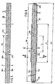
- Figure 6 is a central axial sectional view of a finished detector in accordance with the invention taken in the plane C-C shown in Fig. 3B.
-
- In the process and impedance detector in accordance with the present invention, as the active material, a glass ceramic is used, in which the active constituent in the glass matrix is, for example, crystalline barium-strontium titanate BaxSr1-xTiO3 or crystalline lead-strontium titanate PbxSr1-xTiO3, wherein x is in the range of 0...1. The preparation and the composition of the aluminoborate-based glass used in the detector are preferably similar to those described in the applicant's said FI Patents Nos. 92,441 and 92,439.
- According to Fig. 1, the manufacture of the detector filament takes place by using the pair of
electrode wires reels 30a and 30b, which are provided withfriction brakes 30c, through aquartz crucible 32. The, for example, aluminoborate-basedglass material 11P present in thequartz crucible 32 is prepared by means of methods known from thick-film technology, for example, as follows: - The glass is ground in a ball mill, and it is mixed with an organic constituent, whose composition is, for example, ethyl cellulose (4 %-wt.), Antharox (1.3 %-wt.), and terpineol (94.7 %-wt.). With the above composition, a suitable viscosity is obtained when the proportion of glass powder is ∼ 80 %-wt. and that of the organic constituent ∼ 20 %-wt.
- The drawing
crucible 32 is manufactured, for example, out of a quartz tube, whose end is drawn into a sharp-tipped cone. The end of the cone is cut off so that abottom hole 33 of thecrucible 32 is formed, whose diameter is about 0.3 mm. Theelectrode wires feed reels 30a, 30b provided withfriction brakes 30c, which reels are placed in the drawing device. The ends of thewires wire guide 31, thebottom hole 33 of thequartz crucible 32, and through the drying oven 34 and are fixed to theframe 35 placed in the windingdevice 25. - Onto the bottom of the
crucible 32,glass paste 11P is poured. The windingdevice 25 is started, whereby its motor 39a starts rotating theframe 35 and, at the same time, pulls theelectrode wires crucible 32 at a uniform speed v. When passing through thecrucible 32, theelectrode wires filament 20A passes through the tubular oven 34, in which the temperature is T1≈ 100...150°C. During the winding, at the same time, the windingdevice 25 shifts theframe 35 slowly in the transverse direction (arrow P) so that thewire 20A is wound as screw-shaped over the entire length of theframe 35 in the way shown in Fig. 2. - The winding
device 25 is accomplished, for example, in the way shown in Fig. 1, so that the windingdevice 25 includes a screw motor 39a, which rotates a screw 39b, which is provided with a threading and to which theframe 35 is attached by means of afastening part 38, for example a suitable snap joint. The speed of rotation of the plane andflat frame 35 can be arranged in such a way cyclically varying, for example as sine-formed, that the drawing speed v of thefilament 20A remains invariable. The motor 39a shifts the screw 39b in the direction of the arrow P as the winding of thefilament 20A makes progress. Many other embodiments of the windingdevice 25, which may differ from that shown in Fig. 1 to a substantial extent, are also possible and included in the scope of the invention. - A system that keeps the drawing speed invariable is, however, not necessarily needed in the winding device. The winding device may revolve at an invariable speed, in which case the drawing speed varies as sine-formed. Correspondingly, the coating thickness varies to some extent periodically. The distance of the
frame 35 from thecrucible 32 is dimensioned so that the portions of the filament that are drawn more slowly and that, consequently, have a thicker coating are placed at the edges of theframe 35. In the middle of theframe 35, in the active part of the detector, the coating thickness shows little variation. Said variation is not detrimental in the manufacture of the detector, nor does it deteriorate the reproducibility of the manufacturing process, because it is repeated equally in the case of each detector. - Fig. 3A is a sectional view of a
coated filament 20A after drawing. By regulating thefriction brakes 30c in thereels 30a, 30b (draw tension T), the location of thewire guide 31, the drawing speed v, and/or the temperature T1, it is possible to affect the distance V between theelectrode wires electrode wires - The winding
frame 35 shown in Figs. 1 and 2 has been manufactured by welding out of four thin, e.g., 2mm metal rods longer sides filament 20A to the frame so that, in the later stage of separation of the detector blanks, they can be separated one by one without discharge of the entire filament blank 20A off theframe 35. For theshorter sides frame 35, a metal is suitable best whose thermal expansion coefficient is substantially the same as that of theelectrode wires platinum wires frame 35 is disposable. - After the filament has been wound onto the
frame 35, paste is removed from the ends 42a, 42b of the detector blanks (Fig. 6) over a distance of, for example, about 1 mm by sinking theframe 35, with thelong sides electrode wires detector 40 are made reliably. - The crystallization of the glass-ceramic material 11' on the
detectors 40 also takes place on support of thesame frame 35 by means of a heat treatment similar to that described in the FI Patent 92,439. In the method in which aglass paste 11P is applied, in the first stage of the heat treatment (lower temperature, for example 1 h at 500°C) sintering of the glass paste takes place. In the second stage (higher temperature, for example 1 h at 950°C) the glass is crystallized into a glass-ceramic, which has dielectric properties suitable for the impedance detector. - After the stage of crystallization of the glass-ceramic material 11', in the cutting stage, which is still carried out on the
frame 35, eachelectrode wire wire filament 20B is cut off at onepoint detector 40, i.e. the capacitor to be measured, is formed in the area CV between the cutting-off points electrode wires detector 40 will be connected to its place of operation from its ends so that bothwires - Said cutting-off stage is carried out, for example, in accordance with Fig. 4 by placing the
detector frame 35 on the XYZ-table 54 and by directing thelaser 51 beam LB at the cutting point onto one of theelectrode wires monitor 56 or by using a machine-sight system. For the cutting, a laser is used, e.g. a pulsated Nd/YAG-laser designed for machining use. This laser includes a cutting head, which includes collimation of the laser beam and the optics necessary for the alignment. Theelectrode wire laser 51. After this the beam LB of thelaser 51 is aimed again at the other cut-off point 41a/41b, and a second cutting-off is performed. In this way, all theelectrode wires frame 35 are cut off, after which theframe 35 is turned over, and the same procedure is applied to the detector blanks at the opposite side of the frame. - The active part of the
detector 40 must be protected hermetically from moisture. This is carried out by coating the middle part of thedetector 40 with a layer of glass 12 (Figs. 3B and 6). For the glass layer, a glass paste is used, in which the glass component is some glass whose thermal expansion coefficient is close to that of platinum, such as lead glasses intended for platinum/glass joints, which are available from a number of manufacturers. The organic component in the paste can be the same as in the glass-ceramic paste mentioned above. It is also possible to use ready thick-film pastes intended for hermetic encapsulation. The protective glass paste is spread onto the middle portion of the detector by spraying. As a rule, several, for example four, times of spraying are required from different directions around thefilament 20B. The paste is dried and sintered by using a temperature profile suitable for the paste concerned. The thickness of theprotective glass layer 12 is 10...50 µm whenPt wires detector 40 becomes D1 ≈ 100...150 µm. In Fig. 6, axial lengths L1, L2 and L3 of the detector and of its different parts are indicated. These lengths are chosen, while using the other dimensions given above, e.g., as follows: L1 ≈ 20 mm, L2 ≈ 6 mm, and L3 ≈ 2 mm. - According to Fig. 3B, the cross-sectional shape of the
detector filament 20B and of thefinished detector 40 is elliptical at theprotective layer 12 so that the larger diameter D1 is placed at the centres of theelectrode wires detector filament 20B, besides those shown in the figure, are also possible. - It is only after all of the steps described above that the detector blanks are separated from the
frame 35 by cutting thedetector filaments 20 one at a time from both ends near theframe 35 at points from which theglass layer 11 had been dissolved. In this way, short contact points 42a, 42b of uncoveredelectrode wire detectors 40, from which wires the detector can be fixed easily to its place of operation by soldering or by means of a conductive adhesive. - The advantage of the detector construction described above in comparison to the constructions described in the FI Patent 92,439 is therein that the electrode wires need not be separated from one another and that extra legs need not be removed. This stage is most difficult and the stage most difficult to automatize in the manufacture of the detector constructions described in said patent. The novel construction also makes the detector substantially easier to manufacture in this respect.
- The invention is by no means strictly confined to the process steps described above or to their relative sequence. For example, the relative sequence of the process steps may vary to some extent.
- In the following, the patent claims will be given. The various details of the invention are defined in said claims.
Claims (11)
- A process for manufacture of electrical impedance detectors (40) intended for measurement of physical quantities, in particular of temperature or humidity, in which process a detector filament (20) coated with an active material (11'), whose impedance properties are a function of the physical quantity to be measured, is manufactured, said process comprising the following steps:drawing a pair of electrode wires (10a, 10b) through a paste (11P) at room temperature comprising a starting material of the active material layer (11') and then through a drying oven (34) to produce a filament (20A) with a coating of the starting material;winding the filament (20A) onto a receiving frame (35);crystallizing the active material layer (11') in a separate heat-treatment step that takes place after the winding step;forming at least one detector filament (20) from the filament (20A) by cutting through only one of the electrode wires (10a) at one point (41a) along the length of the filament (20A) and cutting through only the other electrode wire (10b) at another point (41b) along the length of the filament (20A), thus forming a length between the cuts containing the impedance (CM) to be measured; andcutting the filament (20A) to form detector filament pieces containing a detector, and uncovering the electrode wires (10a, 10b) from both ends of said detector filament pieces so as to form electrical contact points (42a, 42b) for the detector (40).
- A process according to Claim 1, wherein the step of drawing comprises drawing the pair of electrode wires through a glass paste.
- A process according to Claim 1, characterized in that said crystallization of the glass paste is carried out on a flat and plate-like frame comprising the receiving frame (35) onto which the filament was wound.
- A process according to Claim 1, characterized in that the crystallization of the active material takes place in two different heat-treatment stages, of which, in the first stage, at a lower temperature, the glass paste is sintered, and in the second stage, which takes place at a higher temperature, the glass material is crystallized into a glass-ceramic material, which has dielectric properties suitable for the impedance detector.
- A process according to Claim 1, characterized in that said cutting step is carried out on a flat and plate-like frame comprising the receiving frame onto which the filament (20) was wound after said coating step.
- A process according to Claim 1, characterized in that, after said winding step, paste is removed from the ends of successive straight portions of the detector filament (20) over a short portion by sinking said frame (35), with its long side (36a, 36b) ahead, into a solvent to form uncovered connecting points of the electrode wires (10a, 10b) at both ends of the pieces of detector filament (20).
- A process according to Claim 6, characterized in that said step of removing paste is carried out in an ultrasound washer.
- A process according to Claim 1, characterized in that said step of cutting through the electrode wires (10a, 10b) is carried out by means of a laser beam (LB) while the detector filament (20) is fixed on said frame (35), so that all the electrode wires (10a, 10b) in the detector filament blanks (20) placed at the top side of the frame are cut through after which the frame (35) is turned over, and the same steps of cutting are applied to the electrode wires (10a, 10b) at the opposite side of the frame.
- A process according to Claim 1, characterized in that an active part of the detector is protected hermetically from moisture by applying onto said part a protective glass layer (12), by applying protective glass paste onto a middle portion of the detector by spraying and by thereupon drying and sintering the protective glass paste.
- A process according to Claim 1, characterized in that the step of cutting the detector filament (20) into separate pieces of detector filament is carried out when the detector filament (20) is placed as wound on said same frame (35).
- A process according to Claim 1, characterized in that, as said frame (35), a rectangular frame is used which is composed of thin metal wires, the filament (20A) being wound as spiral-shaped around long sides (36a, 36b) of said frame while said frame (35) is rotated around a central axis parallel to its long sides and while the frame is, at the same time, displaced (p) in the direction of said axis.
Applications Claiming Priority (2)
| Application Number | Priority Date | Filing Date | Title |
|---|---|---|---|
| FI946117A FI98568C (en) | 1994-12-28 | 1994-12-28 | Electric impedance sensor for measuring physical quantities, especially temperature or humidity and method for producing the sensor in question |
| FI946117 | 1994-12-28 |
Publications (2)
| Publication Number | Publication Date |
|---|---|
| EP0720017A1 EP0720017A1 (en) | 1996-07-03 |
| EP0720017B1 true EP0720017B1 (en) | 2003-06-11 |
Family
ID=8542069
Family Applications (1)
| Application Number | Title | Priority Date | Filing Date |
|---|---|---|---|
| EP95850229A Expired - Lifetime EP0720017B1 (en) | 1994-12-28 | 1995-12-15 | Process for the manufacture of an impedance detector for measurement of physical quantities, in particular of temperature of humidity |
Country Status (6)
| Country | Link |
|---|---|
| US (1) | US5740601A (en) |
| EP (1) | EP0720017B1 (en) |
| JP (1) | JP3625937B2 (en) |
| DE (1) | DE69531039T2 (en) |
| ES (1) | ES2201091T3 (en) |
| FI (1) | FI98568C (en) |
Families Citing this family (1)
| Publication number | Priority date | Publication date | Assignee | Title |
|---|---|---|---|---|
| KR102358881B1 (en) * | 2021-08-25 | 2022-02-08 | (주)케이알바트로스 | Carbon Fiber Filament Inspection Device |
Family Cites Families (9)
| Publication number | Priority date | Publication date | Assignee | Title |
|---|---|---|---|---|
| US2733324A (en) * | 1956-01-31 | B sabouni | ||
| US3168829A (en) * | 1961-10-05 | 1965-02-09 | Honeywell Inc | Control apparatus |
| US3350941A (en) * | 1965-05-20 | 1967-11-07 | Johnson Service Co | Humidity sensing element |
| FR2486656A1 (en) * | 1980-07-09 | 1982-01-15 | Commissariat Energie Atomique | CAPACITIVE HYGROMETER |
| DE3201643A1 (en) * | 1982-01-18 | 1983-07-28 | Siemens AG, 1000 Berlin und 8000 München | Device for locating an ingress of moisture into an elongated object of large extent |
| US5359491A (en) * | 1991-11-27 | 1994-10-25 | U.S. Philips Corporation | Capacitive sensor comprising a conductive front surface for forming a capacitor plate, and a coaxial cable shielded by a mineral insulator |
| FI92441C (en) * | 1992-04-01 | 1994-11-10 | Vaisala Oy | Electronic impedance sensor for measuring physical quantities, in particular temperature, and method of manufacturing that sensor |
| FI92439C (en) * | 1993-09-29 | 1994-11-10 | Vaisala Oy | Electric impedance sensor for measuring physical quantities, especially temperature or humidity and method for producing the sensor in question |
| FI98567C (en) * | 1993-09-29 | 1997-07-10 | Vaisala Oy | Impedance sensor, especially for radio probe use, as well as a method for producing a sensor |
-
1994
- 1994-12-28 FI FI946117A patent/FI98568C/en active
-
1995
- 1995-12-08 US US08/569,867 patent/US5740601A/en not_active Expired - Fee Related
- 1995-12-15 EP EP95850229A patent/EP0720017B1/en not_active Expired - Lifetime
- 1995-12-15 ES ES95850229T patent/ES2201091T3/en not_active Expired - Lifetime
- 1995-12-15 DE DE69531039T patent/DE69531039T2/en not_active Expired - Fee Related
- 1995-12-28 JP JP35313395A patent/JP3625937B2/en not_active Expired - Fee Related
Also Published As
| Publication number | Publication date |
|---|---|
| FI98568B (en) | 1997-03-27 |
| DE69531039D1 (en) | 2003-07-17 |
| JPH08261968A (en) | 1996-10-11 |
| FI946117L (en) | 1996-06-29 |
| DE69531039T2 (en) | 2004-01-29 |
| US5740601A (en) | 1998-04-21 |
| EP0720017A1 (en) | 1996-07-03 |
| FI98568C (en) | 1997-07-10 |
| JP3625937B2 (en) | 2005-03-02 |
| FI946117A0 (en) | 1994-12-28 |
| ES2201091T3 (en) | 2004-03-16 |
Similar Documents
| Publication | Publication Date | Title |
|---|---|---|
| CA2092609C (en) | Electrical impedance detector for measurement of physical quantities | |
| US4361597A (en) | Process for making sensor for detecting fluid flow velocity or flow amount | |
| JP2669932B2 (en) | Signal transmission cable and manufacturing method thereof | |
| EP0647833B1 (en) | Capacitive humidity sensor, in particular for radiosonde operation, as well as a process for the manufacture of a detector | |
| US3939557A (en) | Method of making resistance thermometer sensors | |
| EP0307018A1 (en) | A fuse | |
| EP0645606B1 (en) | Electrically detected impedance detector for the measurement of physical quantities, in particular of temperature or humidity, and process for the manufacture of said detectors | |
| JP3237497B2 (en) | Conductive paste, conductor and ceramic substrate using the same | |
| US5740601A (en) | Method of manufacturing an impedance detector | |
| US3965383A (en) | Multi-wire oxygen electrode and method of manufacturing the same | |
| US4004331A (en) | Method of manufacturing multi-wire oxygen electrode | |
| RU2112966C1 (en) | Multiple microelectrode and process of its manufacture | |
| JPH11162744A (en) | Square air-core coil | |
| GB737853A (en) | Method of producing electrical condensers | |
| JPH0650925A (en) | Manufacture of humidity sensor | |
| JPS62266425A (en) | Manufacture of platinum resistance element | |
| JPH0587824A (en) | Manufacture of heat-sensitive type flow sensor |
Legal Events
| Date | Code | Title | Description |
|---|---|---|---|
| PUAI | Public reference made under article 153(3) epc to a published international application that has entered the european phase |
Free format text: ORIGINAL CODE: 0009012 |
|
| AK | Designated contracting states |
Kind code of ref document: A1 Designated state(s): CH DE DK ES FR GB IT LI SE |
|
| 17P | Request for examination filed |
Effective date: 19961004 |
|
| 17Q | First examination report despatched |
Effective date: 20011211 |
|
| GRAH | Despatch of communication of intention to grant a patent |
Free format text: ORIGINAL CODE: EPIDOS IGRA |
|
| RTI1 | Title (correction) |
Free format text: PROCESS FOR THE MANUFACTURE OF AN IMPEDANCE DETECTOR FOR MEASUREMENT OF PHYSICAL QUANTITIES, IN PARTICULAR OF TEMPERATURE OF HUMIDITY |
|
| GRAH | Despatch of communication of intention to grant a patent |
Free format text: ORIGINAL CODE: EPIDOS IGRA |
|
| RAP1 | Party data changed (applicant data changed or rights of an application transferred) |
Owner name: VAISALA OYJ |
|
| GRAA | (expected) grant |
Free format text: ORIGINAL CODE: 0009210 |
|
| AK | Designated contracting states |
Designated state(s): CH DE DK ES FR GB IT LI SE |
|
| REG | Reference to a national code |
Ref country code: GB Ref legal event code: FG4D |
|
| REG | Reference to a national code |
Ref country code: CH Ref legal event code: EP |
|
| REF | Corresponds to: |
Ref document number: 69531039 Country of ref document: DE Date of ref document: 20030717 Kind code of ref document: P |
|
| REG | Reference to a national code |
Ref country code: CH Ref legal event code: NV Representative=s name: PATENTS & TECHNOLOGY SURVEYS SA |
|
| PG25 | Lapsed in a contracting state [announced via postgrant information from national office to epo] |
Ref country code: SE Free format text: LAPSE BECAUSE OF FAILURE TO SUBMIT A TRANSLATION OF THE DESCRIPTION OR TO PAY THE FEE WITHIN THE PRESCRIBED TIME-LIMIT Effective date: 20030911 Ref country code: DK Free format text: LAPSE BECAUSE OF FAILURE TO SUBMIT A TRANSLATION OF THE DESCRIPTION OR TO PAY THE FEE WITHIN THE PRESCRIBED TIME-LIMIT Effective date: 20030911 |
|
| REG | Reference to a national code |
Ref country code: ES Ref legal event code: FG2A Ref document number: 2201091 Country of ref document: ES Kind code of ref document: T3 |
|
| ET | Fr: translation filed | ||
| PLBE | No opposition filed within time limit |
Free format text: ORIGINAL CODE: 0009261 |
|
| STAA | Information on the status of an ep patent application or granted ep patent |
Free format text: STATUS: NO OPPOSITION FILED WITHIN TIME LIMIT |
|
| 26N | No opposition filed |
Effective date: 20040312 |
|
| PG25 | Lapsed in a contracting state [announced via postgrant information from national office to epo] |
Ref country code: IT Free format text: LAPSE BECAUSE OF NON-PAYMENT OF DUE FEES Effective date: 20051215 |
|
| PGFP | Annual fee paid to national office [announced via postgrant information from national office to epo] |
Ref country code: ES Payment date: 20081205 Year of fee payment: 14 |
|
| PGFP | Annual fee paid to national office [announced via postgrant information from national office to epo] |
Ref country code: DE Payment date: 20081230 Year of fee payment: 14 |
|
| PGFP | Annual fee paid to national office [announced via postgrant information from national office to epo] |
Ref country code: GB Payment date: 20081210 Year of fee payment: 14 Ref country code: CH Payment date: 20090325 Year of fee payment: 14 |
|
| PGFP | Annual fee paid to national office [announced via postgrant information from national office to epo] |
Ref country code: FR Payment date: 20081224 Year of fee payment: 14 |
|
| PGFP | Annual fee paid to national office [announced via postgrant information from national office to epo] |
Ref country code: IT Payment date: 20081222 Year of fee payment: 14 |
|
| PGRI | Patent reinstated in contracting state [announced from national office to epo] |
Ref country code: IT Effective date: 20091201 |
|
| REG | Reference to a national code |
Ref country code: CH Ref legal event code: PL |
|
| GBPC | Gb: european patent ceased through non-payment of renewal fee |
Effective date: 20091215 |
|
| REG | Reference to a national code |
Ref country code: FR Ref legal event code: ST Effective date: 20100831 |
|
| PG25 | Lapsed in a contracting state [announced via postgrant information from national office to epo] |
Ref country code: LI Free format text: LAPSE BECAUSE OF NON-PAYMENT OF DUE FEES Effective date: 20091231 Ref country code: FR Free format text: LAPSE BECAUSE OF NON-PAYMENT OF DUE FEES Effective date: 20091231 Ref country code: CH Free format text: LAPSE BECAUSE OF NON-PAYMENT OF DUE FEES Effective date: 20091231 |
|
| PG25 | Lapsed in a contracting state [announced via postgrant information from national office to epo] |
Ref country code: DE Free format text: LAPSE BECAUSE OF NON-PAYMENT OF DUE FEES Effective date: 20100701 |
|
| PG25 | Lapsed in a contracting state [announced via postgrant information from national office to epo] |
Ref country code: GB Free format text: LAPSE BECAUSE OF NON-PAYMENT OF DUE FEES Effective date: 20091215 |
|
| REG | Reference to a national code |
Ref country code: ES Ref legal event code: FD2A Effective date: 20110304 |
|
| PG25 | Lapsed in a contracting state [announced via postgrant information from national office to epo] |
Ref country code: IT Free format text: LAPSE BECAUSE OF NON-PAYMENT OF DUE FEES Effective date: 20091215 |
|
| PG25 | Lapsed in a contracting state [announced via postgrant information from national office to epo] |
Ref country code: ES Free format text: LAPSE BECAUSE OF NON-PAYMENT OF DUE FEES Effective date: 20110303 |
|
| PG25 | Lapsed in a contracting state [announced via postgrant information from national office to epo] |
Ref country code: ES Free format text: LAPSE BECAUSE OF NON-PAYMENT OF DUE FEES Effective date: 20091216 |