EP0717835B1 - Resonant gauge with microbeam driven in constant electric field - Google Patents
Resonant gauge with microbeam driven in constant electric field Download PDFInfo
- Publication number
- EP0717835B1 EP0717835B1 EP93921396A EP93921396A EP0717835B1 EP 0717835 B1 EP0717835 B1 EP 0717835B1 EP 93921396 A EP93921396 A EP 93921396A EP 93921396 A EP93921396 A EP 93921396A EP 0717835 B1 EP0717835 B1 EP 0717835B1
- Authority
- EP
- European Patent Office
- Prior art keywords
- bias electrode
- electrode
- drive
- flexure element
- bias
- Prior art date
- Legal status (The legal status is an assumption and is not a legal conclusion. Google has not performed a legal analysis and makes no representation as to the accuracy of the status listed.)
- Expired - Lifetime
Links
- 230000005684 electric field Effects 0.000 title claims description 7
- 239000000758 substrate Substances 0.000 claims abstract description 33
- 230000010355 oscillation Effects 0.000 claims abstract description 12
- 239000000463 material Substances 0.000 claims description 6
- 239000004065 semiconductor Substances 0.000 claims description 5
- 238000005468 ion implantation Methods 0.000 claims description 2
- 229910021420 polycrystalline silicon Inorganic materials 0.000 abstract description 23
- 229920005591 polysilicon Polymers 0.000 abstract description 22
- XUIMIQQOPSSXEZ-UHFFFAOYSA-N Silicon Chemical compound [Si] XUIMIQQOPSSXEZ-UHFFFAOYSA-N 0.000 abstract description 9
- 229910052710 silicon Inorganic materials 0.000 abstract description 9
- 239000010703 silicon Substances 0.000 abstract description 9
- 230000003071 parasitic effect Effects 0.000 abstract description 7
- 230000010358 mechanical oscillation Effects 0.000 abstract description 4
- 239000007789 gas Substances 0.000 description 7
- VYPSYNLAJGMNEJ-UHFFFAOYSA-N silicon dioxide Inorganic materials O=[Si]=O VYPSYNLAJGMNEJ-UHFFFAOYSA-N 0.000 description 7
- 230000008901 benefit Effects 0.000 description 6
- BLRPTPMANUNPDV-UHFFFAOYSA-N Silane Chemical compound [SiH4] BLRPTPMANUNPDV-UHFFFAOYSA-N 0.000 description 5
- 239000003990 capacitor Substances 0.000 description 5
- 238000005530 etching Methods 0.000 description 5
- 230000001133 acceleration Effects 0.000 description 4
- 230000004044 response Effects 0.000 description 4
- 229910000077 silane Inorganic materials 0.000 description 4
- 239000010409 thin film Substances 0.000 description 4
- 230000008859 change Effects 0.000 description 3
- 238000000151 deposition Methods 0.000 description 3
- 239000012530 fluid Substances 0.000 description 3
- 238000004518 low pressure chemical vapour deposition Methods 0.000 description 3
- 238000004519 manufacturing process Methods 0.000 description 3
- 230000003647 oxidation Effects 0.000 description 3
- 238000007254 oxidation reaction Methods 0.000 description 3
- 235000012239 silicon dioxide Nutrition 0.000 description 3
- 239000000377 silicon dioxide Substances 0.000 description 3
- RZVAJINKPMORJF-UHFFFAOYSA-N Acetaminophen Chemical compound CC(=O)NC1=CC=C(O)C=C1 RZVAJINKPMORJF-UHFFFAOYSA-N 0.000 description 2
- ZOXJGFHDIHLPTG-UHFFFAOYSA-N Boron Chemical compound [B] ZOXJGFHDIHLPTG-UHFFFAOYSA-N 0.000 description 2
- 229910052581 Si3N4 Inorganic materials 0.000 description 2
- 230000015572 biosynthetic process Effects 0.000 description 2
- 229910052796 boron Inorganic materials 0.000 description 2
- 230000008878 coupling Effects 0.000 description 2
- 238000010168 coupling process Methods 0.000 description 2
- 238000005859 coupling reaction Methods 0.000 description 2
- 230000008021 deposition Effects 0.000 description 2
- 230000000694 effects Effects 0.000 description 2
- 230000005284 excitation Effects 0.000 description 2
- 239000011521 glass Substances 0.000 description 2
- 238000002513 implantation Methods 0.000 description 2
- 238000000034 method Methods 0.000 description 2
- 230000001590 oxidative effect Effects 0.000 description 2
- 230000000737 periodic effect Effects 0.000 description 2
- 230000002093 peripheral effect Effects 0.000 description 2
- 238000001020 plasma etching Methods 0.000 description 2
- 239000005297 pyrex Substances 0.000 description 2
- HQVNEWCFYHHQES-UHFFFAOYSA-N silicon nitride Chemical compound N12[Si]34N5[Si]62N3[Si]51N64 HQVNEWCFYHHQES-UHFFFAOYSA-N 0.000 description 2
- XDTMQSROBMDMFD-UHFFFAOYSA-N Cyclohexane Chemical compound C1CCCCC1 XDTMQSROBMDMFD-UHFFFAOYSA-N 0.000 description 1
- 231100000136 action limit Toxicity 0.000 description 1
- 238000013459 approach Methods 0.000 description 1
- QVGXLLKOCUKJST-UHFFFAOYSA-N atomic oxygen Chemical compound [O] QVGXLLKOCUKJST-UHFFFAOYSA-N 0.000 description 1
- 239000000919 ceramic Substances 0.000 description 1
- 239000013078 crystal Substances 0.000 description 1
- 239000008367 deionised water Substances 0.000 description 1
- 229910021641 deionized water Inorganic materials 0.000 description 1
- 230000001419 dependent effect Effects 0.000 description 1
- 238000010790 dilution Methods 0.000 description 1
- 239000012895 dilution Substances 0.000 description 1
- 230000009977 dual effect Effects 0.000 description 1
- 230000007613 environmental effect Effects 0.000 description 1
- 230000001747 exhibiting effect Effects 0.000 description 1
- 239000010408 film Substances 0.000 description 1
- 238000001914 filtration Methods 0.000 description 1
- 238000012423 maintenance Methods 0.000 description 1
- 238000005259 measurement Methods 0.000 description 1
- 229910021421 monocrystalline silicon Inorganic materials 0.000 description 1
- 239000012299 nitrogen atmosphere Substances 0.000 description 1
- 230000003287 optical effect Effects 0.000 description 1
- 230000003534 oscillatory effect Effects 0.000 description 1
- 239000001301 oxygen Substances 0.000 description 1
- 229910052760 oxygen Inorganic materials 0.000 description 1
- 229920003023 plastic Polymers 0.000 description 1
- 239000004033 plastic Substances 0.000 description 1
- 230000008569 process Effects 0.000 description 1
- 238000012545 processing Methods 0.000 description 1
- 239000010453 quartz Substances 0.000 description 1
- 230000035945 sensitivity Effects 0.000 description 1
- 239000000243 solution Substances 0.000 description 1
- 238000000859 sublimation Methods 0.000 description 1
- 230000008022 sublimation Effects 0.000 description 1
- XLYOFNOQVPJJNP-UHFFFAOYSA-N water Chemical compound O XLYOFNOQVPJJNP-UHFFFAOYSA-N 0.000 description 1
Images


Classifications
-
- G—PHYSICS
- G01—MEASURING; TESTING
- G01P—MEASURING LINEAR OR ANGULAR SPEED, ACCELERATION, DECELERATION, OR SHOCK; INDICATING PRESENCE, ABSENCE, OR DIRECTION, OF MOVEMENT
- G01P15/00—Measuring acceleration; Measuring deceleration; Measuring shock, i.e. sudden change of acceleration
- G01P15/02—Measuring acceleration; Measuring deceleration; Measuring shock, i.e. sudden change of acceleration by making use of inertia forces using solid seismic masses
- G01P15/08—Measuring acceleration; Measuring deceleration; Measuring shock, i.e. sudden change of acceleration by making use of inertia forces using solid seismic masses with conversion into electric or magnetic values
- G01P15/097—Measuring acceleration; Measuring deceleration; Measuring shock, i.e. sudden change of acceleration by making use of inertia forces using solid seismic masses with conversion into electric or magnetic values by vibratory elements
-
- G—PHYSICS
- G01—MEASURING; TESTING
- G01B—MEASURING LENGTH, THICKNESS OR SIMILAR LINEAR DIMENSIONS; MEASURING ANGLES; MEASURING AREAS; MEASURING IRREGULARITIES OF SURFACES OR CONTOURS
- G01B7/00—Measuring arrangements characterised by the use of electric or magnetic techniques
- G01B7/16—Measuring arrangements characterised by the use of electric or magnetic techniques for measuring the deformation in a solid, e.g. by resistance strain gauge
-
- G—PHYSICS
- G01—MEASURING; TESTING
- G01L—MEASURING FORCE, STRESS, TORQUE, WORK, MECHANICAL POWER, MECHANICAL EFFICIENCY, OR FLUID PRESSURE
- G01L1/00—Measuring force or stress, in general
- G01L1/18—Measuring force or stress, in general using properties of piezo-resistive materials, i.e. materials of which the ohmic resistance varies according to changes in magnitude or direction of force applied to the material
- G01L1/183—Measuring force or stress, in general using properties of piezo-resistive materials, i.e. materials of which the ohmic resistance varies according to changes in magnitude or direction of force applied to the material by measuring variations of frequency of vibrating piezo-resistive material
-
- G—PHYSICS
- G01—MEASURING; TESTING
- G01L—MEASURING FORCE, STRESS, TORQUE, WORK, MECHANICAL POWER, MECHANICAL EFFICIENCY, OR FLUID PRESSURE
- G01L9/00—Measuring steady of quasi-steady pressure of fluid or fluent solid material by electric or magnetic pressure-sensitive elements; Transmitting or indicating the displacement of mechanical pressure-sensitive elements, used to measure the steady or quasi-steady pressure of a fluid or fluent solid material, by electric or magnetic means
- G01L9/0001—Transmitting or indicating the displacement of elastically deformable gauges by electric, electro-mechanical, magnetic or electro-magnetic means
- G01L9/0008—Transmitting or indicating the displacement of elastically deformable gauges by electric, electro-mechanical, magnetic or electro-magnetic means using vibrations
- G01L9/0019—Transmitting or indicating the displacement of elastically deformable gauges by electric, electro-mechanical, magnetic or electro-magnetic means using vibrations of a semiconductive element
-
- Y—GENERAL TAGGING OF NEW TECHNOLOGICAL DEVELOPMENTS; GENERAL TAGGING OF CROSS-SECTIONAL TECHNOLOGIES SPANNING OVER SEVERAL SECTIONS OF THE IPC; TECHNICAL SUBJECTS COVERED BY FORMER USPC CROSS-REFERENCE ART COLLECTIONS [XRACs] AND DIGESTS
- Y10—TECHNICAL SUBJECTS COVERED BY FORMER USPC
- Y10S—TECHNICAL SUBJECTS COVERED BY FORMER USPC CROSS-REFERENCE ART COLLECTIONS [XRACs] AND DIGESTS
- Y10S73/00—Measuring and testing
- Y10S73/01—Vibration
Definitions
- the present invention relates to transducers that utilize induced strain as a means for measuring acceleration, pressure, temperature and other variables, and more particularly to transducers employing resonant beams as sensors.
- Resonant sensors have been used for many years to achieve high accuracy measurements. Vibrating transducers have been used in accelerometers, pressure transducers, mass flow sensors, temperature and humidity sensors, air density sensors and scales. These sensors operate on the principle that the natural frequency of vibration (i.e. resonant frequency of an oscillating beam or other member) is a function of the induced strain along the member. More particularly, tensile forces tending to elongate the beam increase its resonant frequency, while forces tending to compress the beam reduce the natural frequency. The frequency output of resonant gauges is readily convened to digital readings reflecting the measured quantity, requiring only a counter and a reference clock for this purpose. Thus, such gauges are simple and reliable, providing a high degree of discrimination while using a relatively simple sensor to digital interface.
- U.S. Patent No. 5,090,254 discloses a resonant beam transducer including a polysilicon beam mounted to a substrate for vibration relative to the substrate, and a polysilicon shell surrounding the beam and affixed to the substrate to form a cavity which is sealed and evacuated.
- the beam is oscillated by supplying an oscillating voltage to an electrode on the shell.
- U.S. Patent No. 3,657,667 discloses a mechanical vibrator having three parallel arms and three piezoelectric elements, one glued to each of the arms. The element on one of the outer arms is used to drive the vibrator, while the remaining piezoelectric elements provide a pair of sensors. The sensors provide an input to an amplifier, with the output of the amplifier being provided to the drive piezoelectric element.
- Resonating members also have been driven magnetically.
- U.S. Patent No. 4, 801,897 (Flecken)
- a magnet is mounted to each of two parallel fluid carrying tubes.
- a coil magnet positioned between the two tube magnets, is actuated by an excitation circuit to oscillate the tubes.
- Optical sensors determine the positions of the oscillating tubes, and provide position information as input to the excitation circuit.
- a dual vibrating beam force transducer is shown in U.S. Patent No. 4,901,586 (Blake et al).
- a pair of parallel beams are positioned between a pair of electrodes.
- a drive circuit provides an oscillating voltage to the electrodes to electrostatically drive the beams, causing the beams to oscillate in a plane containing both beams. The mechanical resonance of the beams controls the oscillation frequency.
- one of two parallel beams is grounded while a drive circuit applies an oscillating voltage to the other beam, thus electrostatically oscillating both beams.
- resonant gauges One of the primary advantages of resonant gauges is that the resonant frequency depends only on the geometrical and mechanical properties of the oscillating beam, and is virtually independent of electrical properties. As a result, precise values (e.g. resistance and capacitance) of drive and sense electrodes are not critical. A possible disadvantage is that any parasitic coupling between the drive and sense electrodes may diminish accuracy of the resonant gauge. Furthermore, in a conventional capacitive drive arrangement, the force between the oscillating beam and drive electrode is quadratic, resulting in an unwanted frequency pulling effect. While crystalline quartz piezoresistors have been satisfactorily employed in resonant gauge applications, their size limits their practical utility.
- a resonant microbeam is disclosed in an article by J. D. Zook in "Sensors and actuators" Volume A35 number 1 of 1 October 1992.
- the present invention provides strain sensing apparatus as defined in Claim 1 hereinafter.
- the present invention may also provide any one or more of the features of dependent Claims 2 to 6 hereinafter.
- the drive signal varies about a center voltage level approximately midway between the first voltage level and the second voltage level. More particularly, the center voltage level is equal to ground, with the first and second voltage levels being at least approximately equal in level and having opposite polarity. In this event, it is advantageous to locate the flexure member approximately transversely centered between the first and second bias electrodes.
- the position sensing means can include a piezoresistor formed on the beam or other flexure member and electrically isolated from the drive electrode.
- the piezoresistor can be coplanar with and spaced apart from the drive electrode.
- the piezoresistor preferably is biased symmetrically with respect to ground.
- the drive electrode is "normally" at ground in the sense that the drive voltage is oscillated about ground. This eliminates a DC bias between the piezoresistor and the drive electrode, and thus eliminates any electrostatic deflection that might rise due to such bias.
- the bias electrodes act as shields for AC voltages, and thus reduce any parasitic capacitance between the drive electrode and the sense electrode (piezoresistor).
- an auxiliary shield electrode can be formed on the beam between the drive electrode and the piezoresistor.
- the shield electrode is maintained at a fixed d.c. potential and at a.c. ground, and forms a "Faraday" shield.
- the beam or other resonating member preferably oscillates in a vacuum, to minimize external environmental influences upon frequency readings.
- the cover and substrate can cooperate to form a fluid tight enclosure containing the beam.
- the substrate, cover and beam all can be formed of semiconductor materials. More particularly, the preferred substrate is silicon.
- the beam and cover are formed of separate polysilicon thin films deposited upon the substrate, with appropriate sacrificial layers subsequently removed by etching to define the beam.
- the beam is microscopic in scale. In one example, the beam has a length of about 300 micrometers, a width of about 30 micrometers and a thickness of about 2 micrometers.
- the substrate and cover can be sized, such that the entire resonant gauge is substantially smaller than a conventional gauge based on a single crystal piezoresistor, e.g. about 0.5 centimeters in its major dimension.
- Formation of the oscillatory beam by etching provides the further advantage that the beam and structure directly supporting it are of the same material. This eliminates errors arising due to interfacing of the beam with different materials supporting the beam.
- the monolithic structure can be formed by combinations of well-known semiconductor processing steps, such as low pressure chemical vapor deposition (LPCVD) for depositing polysilicon and sacrificial layers, and etching steps for removing the sacrificial layers to define the beam.
- LPCVD low pressure chemical vapor deposition
- Silane gas, LPCDV silicon nitride or an oxidizing gas can be used to seal the enclosure about the beam.
- the result is a highly accurate and stable resonant gauge capable of functioning over wide ranges of frequencies and temperature fluctuations.
- the gauges have been found to be highly sensitive as well, for example exhibiting a ratio of change in frequency to resonant frequency of up to 1500 times strain (change in length divided by nominal length).
- resonant gauges in accordance with the present invention are reliable, can be manufactured at relatively low cost, and can be used in a wide variety of demanding applications.
- FIG. 1 to 9 a prior art pressure sensing device 16.
- the device includes a silicon substrate or base 18 including a rigid peripheral rim 20 and a diaphragm 22 surrounded by the rim.
- the diaphragm has a diameter in the range of 25-100 mils, and is flexible and thin, e.g. having a thickness in the range of 10-80 micrometers.
- the bottom of rim 20 is thermoelectrically bonded to a tube 24 of Pyrex (brand) glass or other suitable material, e.g. ceramics, mullites, certain plastics and silicon.
- Tube 24 is supported within a base 26.
- a cover 28 is fastened to the base, and cooperates with the base to define a chamber 30.
- sensing device 16 is positioned at the interface of chamber 30 and the interior of tube 24.
- a pressure responsive resonant strain gauge 32 is mounted on the top of sensing device 16, to diaphragm 22 near peripheral rim 20.
- a substantially similar resonant gauge 34 is mounted to the sensing device at rim 20, and accordingly does not respond to flexure of the diaphragm.
- Gauge 34 is thus usable as a reference, for "filtering out” any movements of gauge 32 in response to factors other than pressure induced diaphragm flexure, e.g. changes in temperature.
- diaphragm 22 is circular, although it is to be appreciated that the diaphragm can be formed with an alternative shape, e.g. square or rectangular, if desired.
- resonant gauge 32 includes an elongate beam 36 formed of fine grain, low tensile strain polysilicon (polycrystalline silicon).
- Beam 36 has a length in the range of 100-1,000 micrometers, and more preferably about 200 micrometers, a thickness (vertical direction in Figures 4 and 5) of about 2 micrometers, and a width of about 40 micrometers.
- Opposite ends of the beam, indicated at 38 and 40, are fixed between substrate 18 (more particularly the diaphragm) and a substantially rigid shell or cover 42, also formed of polysilicon.
- a medial region 44 of the beam is free to oscillate within a chamber 46 formed by the cover and substrate.
- An upper bias electrode 48 is formed (e.g. by implantation) onto a surface portion of cover 42, and a similar lower bias electrode 50 is formed onto a surface of diaphragm 22 along the bottom of chamber 46.
- Electrode 50 is isolated from substrate 18 by fabrication of a PN junction. All electrodes can be isolated from one another by PN junctions or insulative layers, e.g. silicon nitride.
- a drive electrode 52 is formed along a portion of the top surface of beam 36.
- a piezoresistor 54 also is formed along the top surface of the beam and is coplanar with drive electrode 52, spaced apart from electrode 52 and therefore electrically isolated from the drive electrode.
- Bias electrodes 48 and 50 are spaced apart from drive electrode 52 transversely with respect to the length or longitudinal dimension of the beam, with drive electrode 52 approximately transversely centered between the bias electrodes.
- beam 36 is formed as part of a larger polysilicon thin film 56, with longitudinal gaps 58 and 60 extending along opposite sides of the beam.
- Drive electrode 52 is substantially rectangular, although the shape is not critical.
- Piezoresistor 54 includes contact pads 62 and 64, a pair of relatively thin legs 66 and 68. The legs extend into the beam medial region from the pads to an enlarged portion 70 electrically associating the legs. Legs 66 and 68, of course, have a substantially greater resistivity than enlarged portion 70. Accordingly, virtually all of the voltage differential between pads 62 and 64 occurs across the legs, facilitating maintenance of enlarged portion 70 at a desired voltage level, preferably ground.
- Pressure sensing device 16 measures a pressure differential (i.e. the difference between pressures p 1 and p 2 on opposite sides of diaphragm 22), based on the frequency at which beam 36 oscillates. More particularly, flexure of diaphragm 22 produces axial stress upon beam 36, introducing strain along the beam. Downward flexure of diaphragm 22 tends to elongate beam 36 and increase its natural resonant frequency. Conversely, upward diaphragm deflection tends to compress the beam and reduce the resonant frequency.
- a pressure differential i.e. the difference between pressures p 1 and p 2 on opposite sides of diaphragm 22
- a periodically oscillating voltage level is provided to drive electrode 52, while a substantially uniform and constant electrical field is maintained in the region about the beam.
- bias electrode 48 is maintained at a constant positive voltage level +V, while bias electrode 50 is maintained at a constant voltage level -V.
- the bias electrodes have voltages of equal magnitude but of opposite polarity.
- Drive electrode 52 is maintained at ground, with the drive voltage oscillating about ground.
- a negative voltage deflects beam 36 upwardly, due to the attraction to bias electrode 48.
- the attractive force is proportional to the drive voltage, the bias field, and the capacitance of drive electrode 52. Given that the drive electrode capacitance and bias field are substantially constant, the attractive force varies linearly with the drive voltage. While bias electrodes can be maintained at +15 volts and -15 volts, it has been found satisfactory to maintain the bias electrodes at levels as low as a fraction of a volt, with drive voltage amplitudes of less than 1 millivolt.
- the linear behavior is advantageous, in that the sinusoidal oscillation of the drive voltage signal corresponds to the mechanical oscillation of beam 36.
- an approach in which a grounded drive electrode is driven by a periodically oscillating voltage applied to one of the bias electrodes results in a quadratic force between the bias electrode and the electrode on the beam. This gives rise to an undesirable second harmonic distortion and tendency to drive the beam at twice the applied frequency, and can lead to overdrive of the beam and a shift in resonant frequency or undesirable hysteresis.
- a salient advantage is the application of an oscillating drive current to the beam within a constant and uniform electric field, whereby the oscillation of the drive signal more closely corresponds to the mechanical oscillations of the beam.
- Piezoresistor 54 functions as a means for detecting the instantaneous position of beam 36 relative to the substrate and cover, in generating a detector voltage that varies with the beam position.
- the manner in which the piezoresistor generates the detector voltage is known in the art, and not further discussed herein.
- the detector voltage is provided as an input to an oscillator circuit, the output of which is the periodic drive voltage signal.
- the drive voltage signal is provided to drive electrode 52 to maintain beam 36 in steady state oscillation at its fundamental resonant frequency.
- the resonant frequency can be within a range of 100 kHz to 2 MHz, and tends to operate within the narrower range of 200-500 kHz. Since the silicon is not piezoelectric, the beam is driven (i.e. oscillated) by the electrostatic force between each of the bias electrodes and the drive electrode. In either case, one of the bias electrodes and the drive electrode behave as two plates of a capacitor.
- the oscillator circuit shown schematically in Figure 7, provides a closed loop for continually adjusting the frequency of the drive signal toward coincidence with the natural resonant frequency at which beam 36 is oscillating.
- Bias electrodes 48 and 50 are biased at levels +V and -V, respectively, to generate the required uniform and constant electric field in the region about beam 36, and more particularly about drive electrode 52.
- Resistances 72 and 74 are approximately equal in value, to bias the drive electrode at round, i.e. midway between the bias voltage.
- piezoresistor 54 provides the detector signal as an input to an amplifier 76.
- the detector signal is an instantaneous reading of the beam position, in the form of a voltage that oscillates at the same frequency as the frequency of beam oscillation.
- An automatic gain control circuit 78 provides feedback to amplifier 76, to prevent distortion at the oscillation frequency.
- the drive voltage signal is based upon the output of amplifier 76. More particularly, the amplifier output is coupled through a resistance 82 and a capacitor 84 to a circuit including diodes 86 and 88. The diodes cooperate with resistance 82 to clamp the signal amplitude. The clamp action limits oscillation of beam 36 to amplitudes within the linear response range.
- a potentiometer 90 enables fine tuning or adjustment of the drive voltage signal, in terms of average amplitude. Other automatic gain control methods are equally applicable, and are known to those skilled in the art.
- the output of amplifier 76 also is provided to an output buffer amplifier 92.
- the buffer amplifier output is provided to a digital counter 94, which also receives a clocking input from an oscillator 96.
- the output of counter 94 is provided to further digital circuitry, for a direct, real-time reading of strain, pressure, or other parameter that depends upon the resonant frequency of beam 36 as it oscillates.
- a conventional single crystal silicon piezoresistor has a gauge factor typically in the range of about 60-100, depending on doping and orientation. This gauge factor, measured in terms of resistance (r/r) compared to strain (l/l) in any event is less than about 120.
- Pressure sensing devices such as device 16 are manufactured by the equipment already available in the fabrication of semiconductor chips. More particularly, the process begins with a silicon wafer 98 from which a plurality of the sensing devices are fabricated.
- the material is preferably n-type silicon.
- the first step involves forming multiple planar troughs on one side of the wafer, one trough corresponding to each device.
- a bias electrode 99 is formed in each trough 101.
- a lower sacrificial layer of silicon dioxide (SiO 2 ) is formed by local oxidation as indicated at 100 in Figure 8. Further oxidation at this stage forms etch channels.
- a thin film layer of fine grain, low stress polysilicon 102 is deposited onto the wafer substrate 98 and the sacrificial layer, preferably by low pressure chemical vapor deposition.
- a drive electrode 104, a piezoresistor 106, and the necessary electrical leads for these components are formed upon polysilicon layer 102 by boron implantation, more particularly in the region that eventually comprises a beam 106.
- Polysilicon is selectively removed from layer 102 by reactive ion etching, to define beam 106 and remove the polysilicon from above the etch channels.
- a sacrificial layer 108 of low temperature oxide is deposited onto polysilicon layer 102.
- a second layer of polysilicon 110 is deposited to form a cover.
- the polysilicon layers preferably are deposited at a temperature of about 580°C, to form an amorphous (rather than polycrystalline) film.
- an upper bias electrode 112 is formed by boron ion implantation.
- etch channel openings are formed by reactive ion etching. Then, sacrificial layers 100 and 108 are removed by HF etching to form a chamber 114 ( Figure 9).
- the HF residue is removed by a rinse, preferably a deionized water dilution of cyclohexane. To overcome the tendency of beam 106 to adhere to cover 110 due to the HF residue, the rinse solution is frozen, and later removed in a sublimation step to ensure that beam 106 remains free standing.
- the vacuum and the fluid seal necessary to maintain it, can be achieved by exposure of the chamber and channel surface areas to silane (SiH 4 ) gas. Such exposure causes polysilicon to grow along exposed surface areas until it closes off the channel. Trapped silane gas continues to deposit polysilicon within chamber 114 along the chamber walls, until the silane gas is depleted.
- silane SiH 4
- exposed surface areas can be oxidized.
- the resultant growth of silicon dioxide seals the etched channels. Some of the oxidizing gas remains trapped in chamber 114, and oxidation continues until oxygen within the chamber is depleted.
- the device is metalized and annealed in a nitrogen atmosphere at about 450°C, to provide electrical contact to the piezoresistor, beam, and bias electrodes.
- the back of the wafer is patterned, e.g. by isotropic etching, to form the diaphragm portion of each pressure sensing device.
- the wafer is diced into individual chips, whereupon each chip is thermoelectrically bonded to a Pyrex glass tube.
- Figure 10 shows another resonant gauge 116 which is not embodying the present invention and including a silicon substrate 118, a polysilicon thin film layer 120 including a beam 122, and a polysilicon cover 124 cooperating with the substrate to enclose beam 122 within a vacuum chamber 126.
- Upper and lower bias electrodes are formed onto the cover and substrate at 128 and 130, respectively.
- a drive electrode 132 and a position sensing piezoresistor 134 are formed along the top surface of beam 122.
- the bias electrodes act as shields for AC voltages, reducing the parasitic capacitance between the drive electrode and the piezoresistor.
- the chance for parasitic capacitance is further reduced by forming a shield electrode 136 on beam 122 between the drive electrode and piezoresistor.
- Shield electrode 136 preferably is maintained at ground. The grounded shield electrode thus provides a further shield for AC voltages.
- FIG 11 illustrates an alternative use for a resonant strain gauge 138, namely in an accelerometer 140.
- Accelerometer 140 includes a silicon substrate 142 secured to a rigid base 144.
- the substrate includes a substantially rigid mounting portion 146, a substantially rigid proof mass 148, and a relatively narrow neck portion 150 about 0.5-1 mil (12-25 microns) thick between the mounting portion and proof mass.
- Neck portion 150 acts as a bridge, supporting proof mass 148 in cantilever fashion with respect to the rigid mounting portion.
- Resonant strain gauge 138 substantially similar to resonant gauge 116, is mounted to the accelerometer along its top surface at the neck.
- the strain gauge is oriented such that its elongate flexure beam (not shown) extends parallel to the length of neck 150, i.e. left to right as viewed in the figure. Typically, this is perpendicular to the direction of expected acceleration.
- Figure 12 illustrates an embodiment of the resonant strain gauge 152 according to the invention including a substrate 154, an elongate beam 156, and a substantially rigid shell or cover 158. Opposite ends of the beam are fixed to the substrate, and the substrate and cover cooperate to provide a chamber about the beam as previously described, such that a medial region of the beam oscillates within the chamber.
- An upper bias electrode 160 is formed onto a surface portion of the cover, and similar lower bias electrode 162 is formed onto a surface of the substrate along the bottom of the chamber.
- beam 156 is electrically conductive, and thus functions as both the oscillating beam and the beam electrode. Bias electrodes 160 and 162 are spaced apart from beam 156 transversely, with the beam being approximately centered between the bias electrodes.
- bias electrode 160 is maintained at a constant positive voltage level +V through a resistance 164, while lower bias electrode 162 is maintained at a constant voltage level -V through a resistance 166.
- the beam electrode, i.e. beam 156, is maintained at ground.
- An oscillating (a.c.) drive voltage is applied to lower bias electrode 162 through a capacitor 170, which promotes mechanical oscillation of beam 156.
- Bias electrode 160 is coupled to an input of a current sensitive amplifier 172 by a conductive path that includes a capacitor 174. Given the constant level +V, current sensed by amplifier 172 varies with the capacitance between bias electrode 160 and beam 156.
- the absolute magnitude of voltage level V is at least twice the voltage peaks of oscillating drive signal 168.
- the d.c. bias on electrode 162 insures linear behavior and its attendant advantages as previously discussed.
- the d.c. bias on upper electrode 160 permits sensing the position of beam 156 relative to cover 158 (and substrate 154), based on the varying capacitance between electrode 160 and the beam.
- Current to amplifier 172 varies with the capacitance, and thus provides a direct indication of beam position.
- resonant gauge 152 can be incorporated into a circuit similar to that shown schematically in Figure 7, to provide a closed loop for continually adjusting the drive signal frequency toward coincidence with the natural resonant frequency of beam 156.
- a substantially insulative beam and a beam electrode mounted on the beam can be used in lieu of conductive beam 156, if desired.
- the drive electrode and sense electrodes are electrically isolated from one another in a manner that minimizes parasitic capacitance between these electrodes.
- the device is highly sensitive, in that a relatively minor variance in beam strain produces a substantial variance in natural resonant frequency.
- the gauges can be produced as monolithic semiconductor bodies, facilitating formation of microscopic oscillating beams within sealed vacuum chambers, for reliable yet low cost pressure transducers, accelerometers and other instruments.
Landscapes
- Physics & Mathematics (AREA)
- General Physics & Mathematics (AREA)
- Measuring Fluid Pressure (AREA)
- Control Of Motors That Do Not Use Commutators (AREA)
- Logic Circuits (AREA)
- Amplifiers (AREA)
- Measurement Of Current Or Voltage (AREA)
- Metal-Oxide And Bipolar Metal-Oxide Semiconductor Integrated Circuits (AREA)
- Analogue/Digital Conversion (AREA)
Abstract
Description
- The present invention relates to transducers that utilize induced strain as a means for measuring acceleration, pressure, temperature and other variables, and more particularly to transducers employing resonant beams as sensors.
- Resonant sensors have been used for many years to achieve high accuracy measurements. Vibrating transducers have been used in accelerometers, pressure transducers, mass flow sensors, temperature and humidity sensors, air density sensors and scales. These sensors operate on the principle that the natural frequency of vibration (i.e. resonant frequency of an oscillating beam or other member) is a function of the induced strain along the member. More particularly, tensile forces tending to elongate the beam increase its resonant frequency, while forces tending to compress the beam reduce the natural frequency. The frequency output of resonant gauges is readily convened to digital readings reflecting the measured quantity, requiring only a counter and a reference clock for this purpose. Thus, such gauges are simple and reliable, providing a high degree of discrimination while using a relatively simple sensor to digital interface.
- An exemplary use of a vibrating beam transducer is shown in U.S. Patent No. 3,486,383 (Riordan). A pair of parallel beams are employed to limit the angular movement of the gimbal of a gyro. Angular movement in one direction tends to compress the vibrating beams, while angular movement in the opposite direction tends to place the beams under tension. Changes in natural frequency of the beams provide a direct indication of gimbal angular movement.
- U.S. Patent No. 5,090,254 (Guckel et al) discloses a resonant beam transducer including a polysilicon beam mounted to a substrate for vibration relative to the substrate, and a polysilicon shell surrounding the beam and affixed to the substrate to form a cavity which is sealed and evacuated. The beam is oscillated by supplying an oscillating voltage to an electrode on the shell.
- U.S. Patent No. 3,657,667 (Nishikubo et al) discloses a mechanical vibrator having three parallel arms and three piezoelectric elements, one glued to each of the arms. The element on one of the outer arms is used to drive the vibrator, while the remaining piezoelectric elements provide a pair of sensors. The sensors provide an input to an amplifier, with the output of the amplifier being provided to the drive piezoelectric element.
- Resonating members also have been driven magnetically. In U.S. Patent No. 4, 801,897 (Flecken), a magnet is mounted to each of two parallel fluid carrying tubes. A coil magnet, positioned between the two tube magnets, is actuated by an excitation circuit to oscillate the tubes. Optical sensors determine the positions of the oscillating tubes, and provide position information as input to the excitation circuit.
- A dual vibrating beam force transducer is shown in U.S. Patent No. 4,901,586 (Blake et al). A pair of parallel beams are positioned between a pair of electrodes. A drive circuit provides an oscillating voltage to the electrodes to electrostatically drive the beams, causing the beams to oscillate in a plane containing both beams. The mechanical resonance of the beams controls the oscillation frequency. In an alternative embodiment (shown in Blake's Figure 7), one of two parallel beams is grounded while a drive circuit applies an oscillating voltage to the other beam, thus electrostatically oscillating both beams.
- One of the primary advantages of resonant gauges is that the resonant frequency depends only on the geometrical and mechanical properties of the oscillating beam, and is virtually independent of electrical properties. As a result, precise values (e.g. resistance and capacitance) of drive and sense electrodes are not critical. A possible disadvantage is that any parasitic coupling between the drive and sense electrodes may diminish accuracy of the resonant gauge. Furthermore, in a conventional capacitive drive arrangement, the force between the oscillating beam and drive electrode is quadratic, resulting in an unwanted frequency pulling effect. While crystalline quartz piezoresistors have been satisfactorily employed in resonant gauge applications, their size limits their practical utility.
- A resonant microbeam is disclosed in an article by J. D. Zook in "Sensors and actuators" Volume A35 number 1 of 1 October 1992.
- The present invention provides strain sensing apparatus as defined in Claim 1 hereinafter.
- The present invention may also provide any one or more of the features of dependent Claims 2 to 6 hereinafter.
- A distinct advantage arises from generating a uniform and constant electric field using a pair of fixed electrodes, while driving the flexure member with an oscillating voltage supplied to a drive electrode on the beam. More particularly, when a sinusoidal drive voltage is applied to the beam, a charge is injected into the drive electrode. A positive voltage provides a positive charge to deflect the beam toward the negative electrode. On the other hand, a negative voltage applied to the beam deflects the beam in the opposite direction, toward the positive bias electrode. The force is proportional to the drive voltage, the bias field, and the drive electrode capacitance. With the latter two values essentially remaining constant, the force is proportional to the drive voltage and varies linearly with the drive voltage. Accordingly, the frequency pull effect of a quadratic drive force is eliminated.
- The drive signal varies about a center voltage level approximately midway between the first voltage level and the second voltage level. More particularly, the center voltage level is equal to ground, with the first and second voltage levels being at least approximately equal in level and having opposite polarity. In this event, it is advantageous to locate the flexure member approximately transversely centered between the first and second bias electrodes.
- The position sensing means can include a piezoresistor formed on the beam or other flexure member and electrically isolated from the drive electrode. For example, the piezoresistor can be coplanar with and spaced apart from the drive electrode. The piezoresistor preferably is biased symmetrically with respect to ground. The drive electrode is "normally" at ground in the sense that the drive voltage is oscillated about ground. This eliminates a DC bias between the piezoresistor and the drive electrode, and thus eliminates any electrostatic deflection that might rise due to such bias.
- The bias electrodes act as shields for AC voltages, and thus reduce any parasitic capacitance between the drive electrode and the sense electrode (piezoresistor). To further reduce the chance for such parasitic coupling, an auxiliary shield electrode can be formed on the beam between the drive electrode and the piezoresistor. The shield electrode is maintained at a fixed d.c. potential and at a.c. ground, and forms a "Faraday" shield.
- The beam or other resonating member preferably oscillates in a vacuum, to minimize external environmental influences upon frequency readings. To this end, the cover and substrate can cooperate to form a fluid tight enclosure containing the beam. The substrate, cover and beam all can be formed of semiconductor materials. More particularly, the preferred substrate is silicon. The beam and cover are formed of separate polysilicon thin films deposited upon the substrate, with appropriate sacrificial layers subsequently removed by etching to define the beam. The beam is microscopic in scale. In one example, the beam has a length of about 300 micrometers, a width of about 30 micrometers and a thickness of about 2 micrometers. The substrate and cover can be sized, such that the entire resonant gauge is substantially smaller than a conventional gauge based on a single crystal piezoresistor, e.g. about 0.5 centimeters in its major dimension. Formation of the oscillatory beam by etching provides the further advantage that the beam and structure directly supporting it are of the same material. This eliminates errors arising due to interfacing of the beam with different materials supporting the beam. The monolithic structure can be formed by combinations of well-known semiconductor processing steps, such as low pressure chemical vapor deposition (LPCVD) for depositing polysilicon and sacrificial layers, and etching steps for removing the sacrificial layers to define the beam. Silane gas, LPCDV silicon nitride or an oxidizing gas can be used to seal the enclosure about the beam. The result is a highly accurate and stable resonant gauge capable of functioning over wide ranges of frequencies and temperature fluctuations. The gauges have been found to be highly sensitive as well, for example exhibiting a ratio of change in frequency to resonant frequency of up to 1500 times strain (change in length divided by nominal length). Thus, resonant gauges in accordance with the present invention are reliable, can be manufactured at relatively low cost, and can be used in a wide variety of demanding applications.
- For a further understanding of the above and other features and advantages, reference is made to the following detailed description and to the drawings, in which:
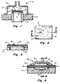
- Figure 1 is an elevational view of a prior art pressure sensing device;
- Figure 2 is a top plan view of the pressure sensing device;
- Figure 3 is a sectional view taken along the line 3-3 in Figure 2;
- Figure 4 is an enlarged view of a portion of Figure 3 showing a resonant gauge of the device;
- Figure 5 is a sectional view taken along the line 5-5 in Figure 4;
- Figure 6 is a top plan view of a resonating beam of the gauge and its surrounding structure, taken along the line 6-6 in Figure 5;
- Figure 7 is a schematic view of the resonant gauge and an associated oscillator circuit;
- Figures 8 and 9 illustrate the resonant gauge at two stages of its fabrication;
- Figure 10 is a sectioned view of another resonant gauge which is not embodying the present invention;
- Figure 11 is a diagrammatic view illustrating an accelerometer employing a resonant gauge in accordance with the present invention, and
- Figure 12 is a schematic view of an alternative embodiment resonant gauge and beam position sensing circuitry.
-
- To enhance understanding of the present invention, there is shown in Figures 1 to 9 a prior art
pressure sensing device 16. The device includes a silicon substrate orbase 18 including a rigidperipheral rim 20 and adiaphragm 22 surrounded by the rim. The diaphragm has a diameter in the range of 25-100 mils, and is flexible and thin, e.g. having a thickness in the range of 10-80 micrometers. The bottom ofrim 20 is thermoelectrically bonded to atube 24 of Pyrex (brand) glass or other suitable material, e.g. ceramics, mullites, certain plastics and silicon.Tube 24 is supported within abase 26. Acover 28 is fastened to the base, and cooperates with the base to define achamber 30. Thus,sensing device 16 is positioned at the interface ofchamber 30 and the interior oftube 24. - A pressure responsive
resonant strain gauge 32 is mounted on the top of sensingdevice 16, to diaphragm 22 nearperipheral rim 20. A substantially similarresonant gauge 34 is mounted to the sensing device atrim 20, and accordingly does not respond to flexure of the diaphragm.Gauge 34 is thus usable as a reference, for "filtering out" any movements ofgauge 32 in response to factors other than pressure induced diaphragm flexure, e.g. changes in temperature. As seen in Figure 2,diaphragm 22 is circular, although it is to be appreciated that the diaphragm can be formed with an alternative shape, e.g. square or rectangular, if desired. - As seen in Figure 4,
resonant gauge 32 includes anelongate beam 36 formed of fine grain, low tensile strain polysilicon (polycrystalline silicon).Beam 36 has a length in the range of 100-1,000 micrometers, and more preferably about 200 micrometers, a thickness (vertical direction in Figures 4 and 5) of about 2 micrometers, and a width of about 40 micrometers. Opposite ends of the beam, indicated at 38 and 40, are fixed between substrate 18 (more particularly the diaphragm) and a substantially rigid shell or cover 42, also formed of polysilicon. Amedial region 44 of the beam is free to oscillate within achamber 46 formed by the cover and substrate. - An
upper bias electrode 48 is formed (e.g. by implantation) onto a surface portion ofcover 42, and a similarlower bias electrode 50 is formed onto a surface ofdiaphragm 22 along the bottom ofchamber 46.Electrode 50 is isolated fromsubstrate 18 by fabrication of a PN junction. All electrodes can be isolated from one another by PN junctions or insulative layers, e.g. silicon nitride. Adrive electrode 52 is formed along a portion of the top surface ofbeam 36. Apiezoresistor 54 also is formed along the top surface of the beam and is coplanar withdrive electrode 52, spaced apart fromelectrode 52 and therefore electrically isolated from the drive electrode.Bias electrodes drive electrode 52 transversely with respect to the length or longitudinal dimension of the beam, withdrive electrode 52 approximately transversely centered between the bias electrodes. - As seen in Figure 6,
beam 36 is formed as part of a larger polysiliconthin film 56, withlongitudinal gaps 58 and 60 extending along opposite sides of the beam.Drive electrode 52 is substantially rectangular, although the shape is not critical.Piezoresistor 54 includescontact pads thin legs enlarged portion 70 electrically associating the legs.Legs enlarged portion 70. Accordingly, virtually all of the voltage differential betweenpads enlarged portion 70 at a desired voltage level, preferably ground. -
Pressure sensing device 16 measures a pressure differential (i.e. the difference between pressures p1 and p2 on opposite sides of diaphragm 22), based on the frequency at whichbeam 36 oscillates. More particularly, flexure ofdiaphragm 22 produces axial stress uponbeam 36, introducing strain along the beam. Downward flexure ofdiaphragm 22 tends to elongatebeam 36 and increase its natural resonant frequency. Conversely, upward diaphragm deflection tends to compress the beam and reduce the resonant frequency. - To maintain the required oscillation of
beam 36, a periodically oscillating voltage level is provided to driveelectrode 52, while a substantially uniform and constant electrical field is maintained in the region about the beam. To this end,bias electrode 48 is maintained at a constant positive voltage level +V, whilebias electrode 50 is maintained at a constant voltage level -V. In other words, the bias electrodes have voltages of equal magnitude but of opposite polarity.Drive electrode 52 is maintained at ground, with the drive voltage oscillating about ground. When the periodic drive voltage (preferably sinusoidal) is applied toelectrode 52, a charge is injected into the drive electrode. A positive voltage injects a positive charge to deflectbeam 36 downwardly, due to the attraction between the drive electrode andnegative bias electrode 50. A negative voltage deflectsbeam 36 upwardly, due to the attraction to biaselectrode 48. In either case, the attractive force is proportional to the drive voltage, the bias field, and the capacitance ofdrive electrode 52. Given that the drive electrode capacitance and bias field are substantially constant, the attractive force varies linearly with the drive voltage. While bias electrodes can be maintained at +15 volts and -15 volts, it has been found satisfactory to maintain the bias electrodes at levels as low as a fraction of a volt, with drive voltage amplitudes of less than 1 millivolt. - The linear behavior is advantageous, in that the sinusoidal oscillation of the drive voltage signal corresponds to the mechanical oscillation of
beam 36. By contrast, an approach in which a grounded drive electrode is driven by a periodically oscillating voltage applied to one of the bias electrodes, results in a quadratic force between the bias electrode and the electrode on the beam. This gives rise to an undesirable second harmonic distortion and tendency to drive the beam at twice the applied frequency, and can lead to overdrive of the beam and a shift in resonant frequency or undesirable hysteresis. Thus, a salient advantage is the application of an oscillating drive current to the beam within a constant and uniform electric field, whereby the oscillation of the drive signal more closely corresponds to the mechanical oscillations of the beam. -
Piezoresistor 54 functions as a means for detecting the instantaneous position ofbeam 36 relative to the substrate and cover, in generating a detector voltage that varies with the beam position. The manner in which the piezoresistor generates the detector voltage is known in the art, and not further discussed herein. - The detector voltage is provided as an input to an oscillator circuit, the output of which is the periodic drive voltage signal. The drive voltage signal is provided to drive
electrode 52 to maintainbeam 36 in steady state oscillation at its fundamental resonant frequency. For a polysilicon beam of the microscopic size described, the resonant frequency can be within a range of 100 kHz to 2 MHz, and tends to operate within the narrower range of 200-500 kHz. Since the silicon is not piezoelectric, the beam is driven (i.e. oscillated) by the electrostatic force between each of the bias electrodes and the drive electrode. In either case, one of the bias electrodes and the drive electrode behave as two plates of a capacitor. - The oscillator circuit, shown schematically in Figure 7, provides a closed loop for continually adjusting the frequency of the drive signal toward coincidence with the natural resonant frequency at which
beam 36 is oscillating.Bias electrodes beam 36, and more particularly aboutdrive electrode 52.Resistances beam 36 mechanically oscillates,piezoresistor 54 provides the detector signal as an input to anamplifier 76. The detector signal is an instantaneous reading of the beam position, in the form of a voltage that oscillates at the same frequency as the frequency of beam oscillation. An automaticgain control circuit 78 provides feedback toamplifier 76, to prevent distortion at the oscillation frequency. - The drive voltage signal, provided to drive
electrode 52 through adrive capacitor 80, is based upon the output ofamplifier 76. More particularly, the amplifier output is coupled through aresistance 82 and acapacitor 84 to acircuit including diodes resistance 82 to clamp the signal amplitude. The clamp action limits oscillation ofbeam 36 to amplitudes within the linear response range. Apotentiometer 90 enables fine tuning or adjustment of the drive voltage signal, in terms of average amplitude. Other automatic gain control methods are equally applicable, and are known to those skilled in the art. - The output of
amplifier 76 also is provided to anoutput buffer amplifier 92. The buffer amplifier output is provided to adigital counter 94, which also receives a clocking input from anoscillator 96. The output ofcounter 94 is provided to further digital circuitry, for a direct, real-time reading of strain, pressure, or other parameter that depends upon the resonant frequency ofbeam 36 as it oscillates. - As noted above, changes in strain along the length (longitudinal dimension) of
beam 36 in response to longitudinally applied external forces, alter the natural resonant frequency of the beam. As the beam begins to oscillate at a different frequency in response to a change in strain, the different frequency is sensed inpiezoresistor 54, and the detector signal is provided toamplifier 76 at the new frequency. The output ofamplifier 76 controls the frequency of the drive voltage signal. In this manner, the drive voltage signal frequency is continually and controllably adjusted toward coincidence with the natural resonant frequency ofbeam 36. In practice, changes in resonant frequency in terms of a base frequency (f/f) have been found to be in the range of 600-1200 times changes in strain or beam elongation (l/l). This provides a high degree of accuracy and sensitivity to slight changes in strain. By comparison, a conventional single crystal silicon piezoresistor has a gauge factor typically in the range of about 60-100, depending on doping and orientation. This gauge factor, measured in terms of resistance (r/r) compared to strain (l/l) in any event is less than about 120. - Pressure sensing devices such as
device 16 are manufactured by the equipment already available in the fabrication of semiconductor chips. More particularly, the process begins with asilicon wafer 98 from which a plurality of the sensing devices are fabricated. The material is preferably n-type silicon. - The first step involves forming multiple planar troughs on one side of the wafer, one trough corresponding to each device. A
bias electrode 99 is formed in eachtrough 101. A lower sacrificial layer of silicon dioxide (SiO2) is formed by local oxidation as indicated at 100 in Figure 8. Further oxidation at this stage forms etch channels. - A thin film layer of fine grain,
low stress polysilicon 102 is deposited onto thewafer substrate 98 and the sacrificial layer, preferably by low pressure chemical vapor deposition. - Following deposition of
polysilicon layer 102, adrive electrode 104, apiezoresistor 106, and the necessary electrical leads for these components are formed uponpolysilicon layer 102 by boron implantation, more particularly in the region that eventually comprises abeam 106. Polysilicon is selectively removed fromlayer 102 by reactive ion etching, to definebeam 106 and remove the polysilicon from above the etch channels. - Following the reactive ion etch, a
sacrificial layer 108 of low temperature oxide is deposited ontopolysilicon layer 102. Then, a second layer ofpolysilicon 110 is deposited to form a cover. The polysilicon layers preferably are deposited at a temperature of about 580°C, to form an amorphous (rather than polycrystalline) film. After deposition oflayer 110, anupper bias electrode 112 is formed by boron ion implantation. - Electrical contact openings and etch channel openings are formed by reactive ion etching. Then,
sacrificial layers beam 106 to adhere to cover 110 due to the HF residue, the rinse solution is frozen, and later removed in a sublimation step to ensure thatbeam 106 remains free standing. - At this point, it is necessary to form a vacuum within
chamber 114. Operation in a vacuum minimizes the possibility of error due to factors other than changes in strain influencing resonant frequency. The vacuum, and the fluid seal necessary to maintain it, can be achieved by exposure of the chamber and channel surface areas to silane (SiH4) gas. Such exposure causes polysilicon to grow along exposed surface areas until it closes off the channel. Trapped silane gas continues to deposit polysilicon withinchamber 114 along the chamber walls, until the silane gas is depleted. - Alternatively, exposed surface areas can be oxidized. The resultant growth of silicon dioxide seals the etched channels. Some of the oxidizing gas remains trapped in
chamber 114, and oxidation continues until oxygen within the chamber is depleted. - With the vacuum and seal thus formed, the device is metalized and annealed in a nitrogen atmosphere at about 450°C, to provide electrical contact to the piezoresistor, beam, and bias electrodes.
- Finally, the back of the wafer is patterned, e.g. by isotropic etching, to form the diaphragm portion of each pressure sensing device. The wafer is diced into individual chips, whereupon each chip is thermoelectrically bonded to a Pyrex glass tube.
- Figure 10 shows another
resonant gauge 116 which is not embodying the present invention and including asilicon substrate 118, a polysiliconthin film layer 120 including abeam 122, and apolysilicon cover 124 cooperating with the substrate to enclosebeam 122 within avacuum chamber 126. Upper and lower bias electrodes are formed onto the cover and substrate at 128 and 130, respectively. Adrive electrode 132 and aposition sensing piezoresistor 134 are formed along the top surface ofbeam 122. - As noted above, the bias electrodes act as shields for AC voltages, reducing the parasitic capacitance between the drive electrode and the piezoresistor. In Figure 10, the chance for parasitic capacitance is further reduced by forming a shield electrode 136 on
beam 122 between the drive electrode and piezoresistor. Shield electrode 136 preferably is maintained at ground. The grounded shield electrode thus provides a further shield for AC voltages. - Figure 11 illustrates an alternative use for a
resonant strain gauge 138, namely in anaccelerometer 140.Accelerometer 140 includes asilicon substrate 142 secured to arigid base 144. The substrate includes a substantially rigid mountingportion 146, a substantiallyrigid proof mass 148, and a relativelynarrow neck portion 150 about 0.5-1 mil (12-25 microns) thick between the mounting portion and proof mass.Neck portion 150 acts as a bridge, supportingproof mass 148 in cantilever fashion with respect to the rigid mounting portion.Resonant strain gauge 138, substantially similar toresonant gauge 116, is mounted to the accelerometer along its top surface at the neck. The strain gauge is oriented such that its elongate flexure beam (not shown) extends parallel to the length ofneck 150, i.e. left to right as viewed in the figure. Typically, this is perpendicular to the direction of expected acceleration. - Acceleration of the device (in particular mounting portion 146), upward as viewed in Figure 11, results in a downward or clockwise deflection of
proof mass 148. The resulting tensile force upongauge 138 imposes strain upon the beam, tending to elongate the beam and raise its natural resonant frequency. The amount of increase in frequency is proportional to the acceleration. Among other examples for such stain gauges are scales (e.g. with a weight suspended from a beam in lieu of proof mass 148), mass flow sensors, temperature sensors, humidity sensors and devices for measuring the density of air or other gases. - Figure 12 illustrates an embodiment of the
resonant strain gauge 152 according to the invention including asubstrate 154, anelongate beam 156, and a substantially rigid shell orcover 158. Opposite ends of the beam are fixed to the substrate, and the substrate and cover cooperate to provide a chamber about the beam as previously described, such that a medial region of the beam oscillates within the chamber. Anupper bias electrode 160 is formed onto a surface portion of the cover, and similarlower bias electrode 162 is formed onto a surface of the substrate along the bottom of the chamber. Ingauge 152,beam 156 is electrically conductive, and thus functions as both the oscillating beam and the beam electrode.Bias electrodes beam 156 transversely, with the beam being approximately centered between the bias electrodes. - A substantially uniform and constant electrical field is maintained in the region about
beam 156. More particularly,bias electrode 160 is maintained at a constant positive voltage level +V through aresistance 164, whilelower bias electrode 162 is maintained at a constant voltage level -V through aresistance 166. The beam electrode, i.e.beam 156, is maintained at ground. - An oscillating (a.c.) drive voltage, indicated at 168, is applied to
lower bias electrode 162 through acapacitor 170, which promotes mechanical oscillation ofbeam 156. - Oscillation of the beam periodically varies the capacitance between the beam and
upper bias electrode 160.Bias electrode 160 is coupled to an input of a currentsensitive amplifier 172 by a conductive path that includes acapacitor 174. Given the constant level +V, current sensed byamplifier 172 varies with the capacitance betweenbias electrode 160 andbeam 156. - To insure substantially linear behavior, the absolute magnitude of voltage level V is at least twice the voltage peaks of oscillating
drive signal 168. The d.c. bias onelectrode 162 insures linear behavior and its attendant advantages as previously discussed. The d.c. bias onupper electrode 160 permits sensing the position ofbeam 156 relative to cover 158 (and substrate 154), based on the varying capacitance betweenelectrode 160 and the beam. Current toamplifier 172 varies with the capacitance, and thus provides a direct indication of beam position. - It is to be understood that
resonant gauge 152 can be incorporated into a circuit similar to that shown schematically in Figure 7, to provide a closed loop for continually adjusting the drive signal frequency toward coincidence with the natural resonant frequency ofbeam 156. Further, a substantially insulative beam and a beam electrode mounted on the beam can be used in lieu ofconductive beam 156, if desired. - Thus, in accordance with the present invention, the drive electrode and sense electrodes are electrically isolated from one another in a manner that minimizes parasitic capacitance between these electrodes. The device is highly sensitive, in that a relatively minor variance in beam strain produces a substantial variance in natural resonant frequency. The gauges can be produced as monolithic semiconductor bodies, facilitating formation of microscopic oscillating beams within sealed vacuum chambers, for reliable yet low cost pressure transducers, accelerometers and other instruments.
Claims (6)
- A strain sensing apparatus, including a rigid substate (154) with a cavity formed on one side, an elongate flexure element (156) coupled across the cavity at a first portion (38/40) so that a second portion (44) is free to oscillate at a resonant frequency, wherein said resonant frequency varies with changes in strain acting upon the flexure element (156), a cover member (158) sealingly fixed to the substrate (154) round a periphery of said elongate flexure element (156) and in cooperation with said cavity to form an enclosed chamber (46) therearound, a first bias electrode region (162), embedded in a surface portion of said cavity and opposing said elongate flexure element (156), wherein said flexure element (156) is spaced apart from said first bias electrode region (162), a second bias electrode region (160) embedded in an exterior surface portion of said cover member (158), a biasing means for biasing the first bias electrode region and the second bias electrode region at respective, different, first and second voltage levels, thereby generating a uniform and constant electrical field around said flexure element (156), the flexure element (156) comprising a beam electrode maintained at ground, an oscillator (168) electrically coupled to one of the first and second bias electrode regions (160, 162), for generating a drive signal comprising a periodically varying/drive voltage signal, to cause oscillation of the elongate flexure (156) relative to the rigid substrate (154) and the cover member (158), means electrically coupled to the other of the first and second bias electrode regions (160, 162) for capacitively generating a position signal of the elongate flexure element (156) relative to the rigid substrate (154), said oscillator(168) receiving said position signal and controllably varying the frequency of the drive signal responsive to variations in the frequency of the position signal, thereby to adjust the drive signal frequency toward coincidence with said resonant frequency.
- Apparatus according to Claim 1 characterised in that the chamber (46) is constructed to maintain a vacuum, relative to ambient pressure.
- Apparatus according to any preceding Claim characterised in that the rigid substrate (154), the flexure element (156), and cover member (158) are formed of a semiconductor material.
- Apparatus according to any preceding Claim characterised in that the first bias electrode region (162), and the second bias electrode region (160) are formed by ion implantation onto the rigid substrate (154) and the cover member (158).
- Apparatus according to any preceding Claim characterised in that the position sensing means comprises a current sensitive amplifier (172) and a conductive path coupled between one of said bias electrode regions (160/162) and the current sensitive amplifier (172), said current sensitive amplifier detecting changes in the current along the conductive path responsive to changes in the capacitance between the beam drive electrode and said one bias electrode region as the flexure element (156) oscillates.
- Apparatus according to any preceding Claim characterised in that said diaphragm (22) is substantially circular, and the flexure element is oriented with its major dimension radially of the diaphragm.
Applications Claiming Priority (2)
| Application Number | Priority Date | Filing Date | Title |
|---|---|---|---|
| US07/937,068 US5275055A (en) | 1992-08-31 | 1992-08-31 | Resonant gauge with microbeam driven in constant electric field |
| PCT/US1993/008404 WO1995007448A1 (en) | 1992-08-31 | 1993-09-07 | Resonant gauge with microbeam driven in constant electric field |
Publications (2)
| Publication Number | Publication Date |
|---|---|
| EP0717835A1 EP0717835A1 (en) | 1996-06-26 |
| EP0717835B1 true EP0717835B1 (en) | 2000-04-26 |
Family
ID=47915796
Family Applications (1)
| Application Number | Title | Priority Date | Filing Date |
|---|---|---|---|
| EP93921396A Expired - Lifetime EP0717835B1 (en) | 1992-08-31 | 1993-09-07 | Resonant gauge with microbeam driven in constant electric field |
Country Status (7)
| Country | Link |
|---|---|
| US (1) | US5275055A (en) |
| EP (1) | EP0717835B1 (en) |
| JP (2) | JPH09502274A (en) |
| AU (1) | AU683850B2 (en) |
| CA (1) | CA2171188C (en) |
| DE (1) | DE69328500T2 (en) |
| WO (1) | WO1995007448A1 (en) |
Families Citing this family (60)
| Publication number | Priority date | Publication date | Assignee | Title |
|---|---|---|---|---|
| US5458000A (en) * | 1993-07-20 | 1995-10-17 | Honeywell Inc. | Static pressure compensation of resonant integrated microbeam sensors |
| US5417115A (en) * | 1993-07-23 | 1995-05-23 | Honeywell Inc. | Dielectrically isolated resonant microsensors |
| US5442962A (en) * | 1993-08-20 | 1995-08-22 | Setra Systems, Inc. | Capacitive pressure sensor having a pedestal supported electrode |
| US5550516A (en) * | 1994-12-16 | 1996-08-27 | Honeywell Inc. | Integrated resonant microbeam sensor and transistor oscillator |
| US5742222A (en) * | 1995-05-26 | 1998-04-21 | Avi Systems, Inc. | Direct adhering polysilicon based strain gage |
| GB2301671B (en) * | 1995-05-30 | 1999-10-13 | Allied Signal Inc | Angular rate sensor electronic balance |
| GB2301669B (en) * | 1995-05-30 | 1999-11-10 | Allied Signal Inc | Angular rate sensor misalignment correction |
| US6021675A (en) * | 1995-06-07 | 2000-02-08 | Ssi Technologies, Inc. | Resonating structure and method for forming the resonating structure |
| EP0753728A3 (en) * | 1995-07-14 | 1998-04-15 | Yokogawa Electric Corporation | Semiconductor differential pressure measuring device |
| US5798502A (en) * | 1996-05-10 | 1998-08-25 | Oak Frequency | Temperature controlled substrate for VLSI construction having minimal parasitic feedback |
| US5772322A (en) * | 1996-05-31 | 1998-06-30 | Honeywell Inc. | Resonant microbeam temperature sensor |
| IT1287123B1 (en) * | 1996-10-31 | 1998-08-04 | Abb Kent Taylor Spa | DEVICE FOR MEASURING A PRESSURE |
| US20040099061A1 (en) * | 1997-12-22 | 2004-05-27 | Mks Instruments | Pressure sensor for detecting small pressure differences and low pressures |
| US6126311A (en) * | 1998-11-02 | 2000-10-03 | Claud S. Gordon Company | Dew point sensor using mems |
| US6215221B1 (en) * | 1998-12-29 | 2001-04-10 | Honeywell International Inc. | Electrostatic/pneumatic actuators for active surfaces |
| US6698295B1 (en) | 2000-03-31 | 2004-03-02 | Shipley Company, L.L.C. | Microstructures comprising silicon nitride layer and thin conductive polysilicon layer |
| US7026697B2 (en) * | 2000-03-31 | 2006-04-11 | Shipley Company, L.L.C. | Microstructures comprising a dielectric layer and a thin conductive layer |
| EP1164378B1 (en) * | 2000-06-16 | 2012-03-14 | Infineon Technologies AG | Acceleration Sensor |
| IT1318295B1 (en) | 2000-07-31 | 2003-07-28 | Abb Ricerca Spa | DEVICE FOR MEASURING THE PRESSURE OF A FLUID |
| US6584857B1 (en) | 2000-11-20 | 2003-07-01 | Eastman Kodak Company | Optical strain gauge |
| US6487913B2 (en) | 2000-12-18 | 2002-12-03 | Eastman Kodak Company | Strain gauge with resonant light modulator |
| FR2818676B1 (en) * | 2000-12-27 | 2003-03-07 | Freyssinet Int Stup | METHOD FOR DISASSEMBLING A PRE-STRESS CABLE AND DEVICE FOR IMPLEMENTING THE SAME |
| US6714102B2 (en) * | 2001-03-01 | 2004-03-30 | Agilent Technologies, Inc. | Method of fabricating thin film bulk acoustic resonator (FBAR) and FBAR structure embodying the method |
| US20040036378A1 (en) * | 2002-08-20 | 2004-02-26 | Rodgers Murray Steven | Dust cover for MEM components |
| EP1588153B1 (en) * | 2002-12-27 | 2007-10-03 | NanoNord A/S | A cantilever sensor using both the longitudinal and the transversal piezoresistive coefficients |
| US6739199B1 (en) | 2003-03-10 | 2004-05-25 | Hewlett-Packard Development Company, L.P. | Substrate and method of forming substrate for MEMS device with strain gage |
| US6993973B2 (en) * | 2003-05-16 | 2006-02-07 | Mks Instruments, Inc. | Contaminant deposition control baffle for a capacitive pressure transducer |
| US7188511B2 (en) * | 2004-06-11 | 2007-03-13 | Robert Bosch Gmbh | Stress wave sensor |
| US7231803B2 (en) * | 2004-06-11 | 2007-06-19 | Robert Bosch Gmbh | Hybrid impact sensor |
| US7623142B2 (en) | 2004-09-14 | 2009-11-24 | Hewlett-Packard Development Company, L.P. | Flexure |
| US7201057B2 (en) * | 2004-09-30 | 2007-04-10 | Mks Instruments, Inc. | High-temperature reduced size manometer |
| US7141447B2 (en) * | 2004-10-07 | 2006-11-28 | Mks Instruments, Inc. | Method of forming a seal between a housing and a diaphragm of a capacitance sensor |
| US7137301B2 (en) * | 2004-10-07 | 2006-11-21 | Mks Instruments, Inc. | Method and apparatus for forming a reference pressure within a chamber of a capacitance sensor |
| US7368312B1 (en) * | 2004-10-15 | 2008-05-06 | Morgan Research Corporation | MEMS sensor suite on a chip |
| US7499604B1 (en) | 2004-12-12 | 2009-03-03 | Burns David W | Optically coupled resonant pressure sensor and process |
| US7605391B2 (en) * | 2004-12-12 | 2009-10-20 | Burns David W | Optically coupled resonator |
| US7443509B1 (en) | 2004-12-12 | 2008-10-28 | Burns David W | Optical and electronic interface for optically coupled resonators |
| US7176048B1 (en) | 2004-12-12 | 2007-02-13 | Burns David W | Optically coupled sealed-cavity resonator and process |
| US7379629B1 (en) | 2004-12-12 | 2008-05-27 | Burns David W | Optically coupled resonant pressure sensor |
| US7017418B1 (en) * | 2004-12-15 | 2006-03-28 | General Electric Company | System and method for sensing pressure |
| US20060134510A1 (en) * | 2004-12-21 | 2006-06-22 | Cleopatra Cabuz | Air cell air flow control system and method |
| US7204150B2 (en) | 2005-01-14 | 2007-04-17 | Mks Instruments, Inc. | Turbo sump for use with capacitive pressure sensor |
| US20070017276A1 (en) * | 2005-07-20 | 2007-01-25 | Trutna William R Jr | Resonant structure humidity sensor |
| US20070236213A1 (en) * | 2006-03-30 | 2007-10-11 | Paden Bradley E | Telemetry method and apparatus using magnetically-driven mems resonant structure |
| FR2919067B1 (en) | 2007-07-19 | 2009-08-28 | Sagem Defense Securite | METHOD FOR MEASURING ACCELERATION USING A PIEZOELECTRIC VIBRANT ACCELEROMETER AND CORRESPONDING MEASURING DEVICE |
| US7661313B2 (en) * | 2007-11-05 | 2010-02-16 | The United States Of America As Represented By The Secretary Of The Navy | Acceleration strain transducer |
| US8468887B2 (en) * | 2008-04-14 | 2013-06-25 | Freescale Semiconductor, Inc. | Resonant accelerometer with low sensitivity to package stress |
| US7589329B1 (en) | 2008-04-23 | 2009-09-15 | Honeywell International Inc. | Systems and methods for remote optical sensing |
| US8076737B2 (en) * | 2008-05-20 | 2011-12-13 | Honeywell International Inc. | Systems and methods for acoustic sensing |
| US8115573B2 (en) * | 2009-05-29 | 2012-02-14 | Infineon Technologies Ag | Resonance frequency tunable MEMS device |
| DE102010030878B4 (en) * | 2010-07-02 | 2023-08-17 | Robert Bosch Gmbh | Micromechanical sensor device for measuring an acceleration, a pressure and the like |
| PT2458357E (en) * | 2010-11-29 | 2014-06-11 | Air Prod & Chem | Method of, and apparatus for, measuring the pressure of a gas |
| US8650963B2 (en) * | 2011-08-15 | 2014-02-18 | Pgs Geophysical As | Electrostatically coupled pressure sensor |
| FR2995995B1 (en) * | 2012-09-26 | 2014-09-19 | Sagem Defense Securite | PRESSURE SENSOR BASED ON NANOJAUGES COUPLEES WITH A RESONATOR |
| JP2014115210A (en) * | 2012-12-11 | 2014-06-26 | Seiko Epson Corp | Mems element, electronic device, altimeter, electronic apparatus and moving body |
| JP2014115208A (en) * | 2012-12-11 | 2014-06-26 | Seiko Epson Corp | Mems element, electronic device, altimeter, electronic apparatus and moving body |
| JP6044607B2 (en) | 2014-08-28 | 2016-12-14 | 横河電機株式会社 | Vibration sensor device |
| US10580605B2 (en) | 2015-11-23 | 2020-03-03 | University Of Utah Research Foundation | Very low power microelectromechanical devices for the internet of everything |
| JP7155035B2 (en) | 2019-02-18 | 2022-10-18 | 株式会社荏原製作所 | Polishing device and polishing method |
| CN112710869B (en) * | 2020-12-09 | 2023-04-21 | 华中光电技术研究所(中国船舶重工集团公司第七一七研究所) | Harmonic oscillator rigid shaft identification device and method based on additional static stiffness principle |
Family Cites Families (9)
| Publication number | Priority date | Publication date | Assignee | Title |
|---|---|---|---|---|
| US3164987A (en) * | 1961-03-28 | 1965-01-12 | Bosch Arma Corp | Electrostatic vibration transducer |
| US3486383A (en) * | 1965-01-04 | 1969-12-30 | Singer General Precision | Vibrating beam transducer |
| US3413573A (en) * | 1965-06-18 | 1968-11-26 | Westinghouse Electric Corp | Microelectronic frequency selective apparatus with vibratory member and means responsive thereto |
| US3470400A (en) * | 1967-12-21 | 1969-09-30 | Singer General Precision | Single beam force transducer with integral mounting isolation |
| CH511476A (en) * | 1968-10-08 | 1971-03-15 | Proctor Ets | Device for generating periodic mechanical vibrations in a clockwork |
| US3657667A (en) * | 1969-04-23 | 1972-04-18 | Citizen Watch Co Ltd | Oscillator with three-arm mechanical vibrator connected to suppress spurious vibrations |
| DE8712331U1 (en) * | 1986-09-26 | 1988-01-28 | Flowtec AG, Reinach, Basel | Coriolis force mass flow meter |
| US4901586A (en) * | 1989-02-27 | 1990-02-20 | Sundstrand Data Control, Inc. | Electrostatically driven dual vibrating beam force transducer |
| US5090254A (en) * | 1990-04-11 | 1992-02-25 | Wisconsin Alumni Research Foundation | Polysilicon resonating beam transducers |
-
1992
- 1992-08-31 US US07/937,068 patent/US5275055A/en not_active Expired - Lifetime
-
1993
- 1993-09-07 WO PCT/US1993/008404 patent/WO1995007448A1/en not_active Ceased
- 1993-09-07 EP EP93921396A patent/EP0717835B1/en not_active Expired - Lifetime
- 1993-09-07 JP JP7508640A patent/JPH09502274A/en active Pending
- 1993-09-07 CA CA002171188A patent/CA2171188C/en not_active Expired - Fee Related
- 1993-09-07 JP JP50864095A patent/JP3223358B2/en not_active Expired - Lifetime
- 1993-09-07 AU AU48502/93A patent/AU683850B2/en not_active Ceased
- 1993-09-07 DE DE69328500T patent/DE69328500T2/en not_active Expired - Lifetime
Also Published As
| Publication number | Publication date |
|---|---|
| DE69328500D1 (en) | 2000-05-31 |
| AU4850293A (en) | 1995-03-27 |
| JPH09502274A (en) | 1997-03-04 |
| WO1995007448A1 (en) | 1995-03-16 |
| US5275055A (en) | 1994-01-04 |
| CA2171188C (en) | 2006-04-18 |
| EP0717835A1 (en) | 1996-06-26 |
| DE69328500T2 (en) | 2000-09-21 |
| CA2171188A1 (en) | 1995-03-16 |
| AU683850B2 (en) | 1997-11-27 |
| JP3223358B2 (en) | 2001-10-29 |
Similar Documents
| Publication | Publication Date | Title |
|---|---|---|
| US5275055A (en) | Resonant gauge with microbeam driven in constant electric field | |
| EP0740781B1 (en) | Compensation of resonant integrated microbeam sensors | |
| US5417115A (en) | Dielectrically isolated resonant microsensors | |
| US5511427A (en) | Cantilevered microbeam temperature sensor | |
| US5772322A (en) | Resonant microbeam temperature sensor | |
| EP0451992B1 (en) | Detection of vibrations of a microbeam through a shell | |
| Burns et al. | Sealed-cavity resonant microbeam pressure sensor | |
| US4945765A (en) | Silicon micromachined accelerometer | |
| US5233874A (en) | Active microaccelerometer | |
| Welham et al. | A laterally driven micromachined resonant pressure sensor | |
| WO1995004265A9 (en) | Dielectrically isolated resonant microsensors | |
| EP0797758B1 (en) | Integrated resonant microbeam sensor and transistor oscillator | |
| US7605391B2 (en) | Optically coupled resonator | |
| JPH0518050B2 (en) | ||
| US5656777A (en) | Miniature box vibrating gyroscope | |
| Kobayashi et al. | Double-frame silicon gyroscope packaged under low pressure by wafer bonding | |
| US7176048B1 (en) | Optically coupled sealed-cavity resonator and process | |
| Langdon | Micromachining of Silicon for Sensors |
Legal Events
| Date | Code | Title | Description |
|---|---|---|---|
| PUAI | Public reference made under article 153(3) epc to a published international application that has entered the european phase |
Free format text: ORIGINAL CODE: 0009012 |
|
| 17P | Request for examination filed |
Effective date: 19960401 |
|
| AK | Designated contracting states |
Kind code of ref document: A1 Designated state(s): DE FR GB |
|
| 17Q | First examination report despatched |
Effective date: 19961002 |
|
| GRAG | Despatch of communication of intention to grant |
Free format text: ORIGINAL CODE: EPIDOS AGRA |
|
| GRAG | Despatch of communication of intention to grant |
Free format text: ORIGINAL CODE: EPIDOS AGRA |
|
| GRAH | Despatch of communication of intention to grant a patent |
Free format text: ORIGINAL CODE: EPIDOS IGRA |
|
| GRAH | Despatch of communication of intention to grant a patent |
Free format text: ORIGINAL CODE: EPIDOS IGRA |
|
| GRAA | (expected) grant |
Free format text: ORIGINAL CODE: 0009210 |
|
| AK | Designated contracting states |
Kind code of ref document: B1 Designated state(s): DE FR GB |
|
| REF | Corresponds to: |
Ref document number: 69328500 Country of ref document: DE Date of ref document: 20000531 |
|
| ET | Fr: translation filed | ||
| PLBE | No opposition filed within time limit |
Free format text: ORIGINAL CODE: 0009261 |
|
| STAA | Information on the status of an ep patent application or granted ep patent |
Free format text: STATUS: NO OPPOSITION FILED WITHIN TIME LIMIT |
|
| 26N | No opposition filed | ||
| REG | Reference to a national code |
Ref country code: GB Ref legal event code: IF02 |
|
| PGFP | Annual fee paid to national office [announced via postgrant information from national office to epo] |
Ref country code: GB Payment date: 20090807 Year of fee payment: 17 |
|
| PGFP | Annual fee paid to national office [announced via postgrant information from national office to epo] |
Ref country code: DE Payment date: 20090930 Year of fee payment: 17 |
|
| GBPC | Gb: european patent ceased through non-payment of renewal fee |
Effective date: 20100907 |
|
| REG | Reference to a national code |
Ref country code: FR Ref legal event code: ST Effective date: 20110531 |
|
| REG | Reference to a national code |
Ref country code: DE Ref legal event code: R119 Ref document number: 69328500 Country of ref document: DE Effective date: 20110401 |
|
| PG25 | Lapsed in a contracting state [announced via postgrant information from national office to epo] |
Ref country code: FR Free format text: LAPSE BECAUSE OF NON-PAYMENT OF DUE FEES Effective date: 20100930 Ref country code: DE Free format text: LAPSE BECAUSE OF NON-PAYMENT OF DUE FEES Effective date: 20110401 |
|
| PG25 | Lapsed in a contracting state [announced via postgrant information from national office to epo] |
Ref country code: GB Free format text: LAPSE BECAUSE OF NON-PAYMENT OF DUE FEES Effective date: 20100907 |
|
| PGFP | Annual fee paid to national office [announced via postgrant information from national office to epo] |
Ref country code: FR Payment date: 20090916 Year of fee payment: 17 |
|
| P01 | Opt-out of the competence of the unified patent court (upc) registered |
Effective date: 20230525 |