EP0714101A2 - An integrated circuit memory device with voltage boost - Google Patents
An integrated circuit memory device with voltage boost Download PDFInfo
- Publication number
- EP0714101A2 EP0714101A2 EP95308018A EP95308018A EP0714101A2 EP 0714101 A2 EP0714101 A2 EP 0714101A2 EP 95308018 A EP95308018 A EP 95308018A EP 95308018 A EP95308018 A EP 95308018A EP 0714101 A2 EP0714101 A2 EP 0714101A2
- Authority
- EP
- European Patent Office
- Prior art keywords
- voltage
- sub
- wordline
- sector
- integrated circuit
- Prior art date
- Legal status (The legal status is an assumption and is not a legal conclusion. Google has not performed a legal analysis and makes no representation as to the accuracy of the status listed.)
- Granted
Links
Images


Classifications
-
- G—PHYSICS
- G11—INFORMATION STORAGE
- G11C—STATIC STORES
- G11C8/00—Arrangements for selecting an address in a digital store
- G11C8/14—Word line organisation; Word line lay-out
-
- G—PHYSICS
- G11—INFORMATION STORAGE
- G11C—STATIC STORES
- G11C16/00—Erasable programmable read-only memories
- G11C16/02—Erasable programmable read-only memories electrically programmable
- G11C16/06—Auxiliary circuits, e.g. for writing into memory
- G11C16/08—Address circuits; Decoders; Word-line control circuits
-
- G—PHYSICS
- G11—INFORMATION STORAGE
- G11C—STATIC STORES
- G11C5/00—Details of stores covered by group G11C11/00
- G11C5/14—Power supply arrangements, e.g. power down, chip selection or deselection, layout of wirings or power grids, or multiple supply levels
Definitions
- the present invention relates to an integrated circuit memory device with a voltage boost facility.
- Integrated circuit memory devices are made which can operate with different power supply voltages.
- a typical memory chip can operate with a power supply voltage of 5V ⁇ 10% or with a power supply voltage of 3.3V ⁇ 0.3V.
- a voltage of approximately 5V is sufficient to deliver enough cell current for reliable sensing in cells having an erase threshold voltage of about 3V which is the highest practical maximum in existing floating gate transistor cells in non-volatile memories.
- the power supply voltage is 5V, the necessary voltage required for reading can be -derived directly from the power supply itself.
- Voltage boost circuits are known and are not discussed in detail herein. They include a boot capacitor across which the output boosted voltage is provided. The boosted level is determined by the ratio of the boot capacitor to the amount of capacitance which is connected on the supply line on which the voltage is to be boosted. If this capacitance can be reduced, then the size of the boot capacitor can be reduced to maintain the ratio thus give the same boosted level. This gives an advantage in a reduction of chip area, time taken to boost the supply voltage, power and on-chip noise generated by the circuit.
- a pump circuit relies on several capacitively coupled stages, isolated by diodes, to progressively raise the voltage to the required level. These stages are driven by non-overlapping clocks. A reduction of the capacitance to be raised is also advantageous for these circuits.
- the power supply line to be boosted is connected to all the cells in a row of the memory and to the peripheral circuits for driving the wordlines.
- the present invention seeks to reduce the capacitance connected to the power supply line when the supply voltage is boosted in order to overcome these problems.
- Random access memories having so-called divided wordline (DWL) architectures are known, in which a wordline is divided into independently addressable sub-wordlines. This improves memory speed by avoiding long wordlines and the associated larger resistances and capacitances. It would be desirable to use DWL architecture in so-called flash memories, that is memories made up of electrically erasable and programmable single floating gate transistor cells, to utilise its speed advantages.
- flash memories that is memories made up of electrically erasable and programmable single floating gate transistor cells, to utilise its speed advantages.
- problems arise in routing different voltage levels to the gates of the cells and keeping sub-wordline drive circuits relatively simple and hence small. It will be appreciated that there is a trade-off between improvement in speed using a DWL architecture and area consumed by the required sub-wordline drive circuits. Problems associated with routing different voltages to the gates of the cells are compounded when the voltage supply level has to be increased by pumping or boosting.
- sub-wordline drive circuits increase the capacitance on the voltage
- an integrated circuit memory device comprising:
- each sector will contain a plurality of sub-wordlines, and one or more groups of sub-wordline drive circuits.
- control circuitry comprises a plurality of voltage control switches, each voltage control switch being associated with a group of sub-wordline drive circuits for applying said cell voltage to a group of sub-wordline drive circuits when a sub-wordline associated with a sub-wordline drive circuit in that group is selected.
- Each voltage control switch can be made responsive to a SECTOR ENABLE signal so that it can be disabled when the sub-wordline drive circuit or sub-wordline drive circuits associated with that voltage switch are not selected.
- the voltage control switch When disabled, the voltage control switch can connect the group of sub-wordline drive circuits to the power supply voltage.
- the integrated circuit memory device can include a plurality of main wordlines extending in the row direction, each main wordline being connected to a plurality of sub-wordline drive circuits in the column direction.
- the row addressing circuitry comprises a main wordline decode circuit for selecting one of said plurality of main wordlines and a sub-wordline decode circuit for selecting a group of said sub-wordline drive circuits.
- the sub-wordline drive circuits connected to each main wordline and extending in the column direction can be arranged in an interleaved fashion with sub-wordline drive circuits associated with alternate sub-wordlines being located on opposite sides of said sector of cells. This relaxes the pitch of the sub-wordline drive circuits and therefore eases layout problems in fitting in the required number of sub-wordline drive circuits.
- the voltage raising circuitry comprises a single voltage boost circuit and a boost capacitor connected between the voltage boost circuit and a common memory voltage supply line.
- the boost capacitor increases the voltage on said common memory voltage supply line above the power supply voltage.
- the boost capacitor extends across the width of the memory array to minimise RC delays on the boosted node.
- the voltage raising circuitry comprises a plurality of voltage boost circuits and associated boost capacitors, wherein each sector of cells has associated therewith at least one voltage boost circuit and a boost capacitor.
- each boost capacitor is connected between its voltage boost circuit and a group of sub-wordline drive circuits of said sector.
- the control circuitry is operative to connect the power supply voltage to the boost capacitor of selected sectors thereby to permit said boost capacitor to supply said cell voltage to a sub-wordline drive circuit of a selected sub-wordline.
- the capacitance of all the control circuitry is connected to the supply line during boosting and this can be a large proportion of the total capacitance. This is eliminated in this alternative embodiment.
- Sector switches can also be provided for selectively applying a boosted power supply voltage to reference circuits which are associated with sense circuitry of each sector.
- control switches and sector switches enables the capacitance associated with the voltage boost circuit to be minimised by connecting to the voltage boost circuit only those elements which are intended to receive the boosted power supply voltage and disconnecting other elements from the line on which the voltage is to be boosted.
- DWL architecture when applied to flash memories arises during programming of the memory, when the gates of all cells connected to a wordline are taken to the programming voltage of 12V. The effect of this is to increase the threshold voltages of erased cells.
- sub-wordlines are only active on a per sector basis and therefore cells are subject to far less stress throughout the lifetime of the part.
- a non-DWL architecture means have to be provided to relieve this stress in non-selected sectors.
- Figure 1 is a schematic diagram of a flash memory array.
- the array consists of a plurality of memory cells extending in rows and columns.
- the array comprises a plurality n of main wordlines MWL0 to MWLn .
- Each main wordline extends along the full width of the memory array in the row direction.
- the memory array also comprises a plurality of bit lines.
- the array is divided into sectors, each sector including a plurality of columns of cells, each column of cells being connected to a respective bit line.
- Each sector has a plurality p of columns and a corresponding plurality p of bit lines which are denoted BL0 to BLp for the first sector SECTOR 1 of the array shown in Figure 1.
- a sub-wordline extends along the width of one sector and is connected to all cells in a row of the sector, in this case p cells.
- each main wordline is associated with four sub-wordlines defining respectively four rows of the sector. These are denoted SWL1, SWL2, SWL3 and SWL4 for the first sector SECTOR 1 shown in Figure 1.
- SWL1, SWL2, SWL3 and SWL4 for the first sector SECTOR 1 shown in Figure 1.
- the main wordline runs on a pitch of four cells, that is there are four cells column wise between each main wordline.
- the pitch of the main wordline is not critical to the present invention and any suitable pitch could be selected, subject to limitations of the process used to manufacture the memory device. In particular, pitches of 2,4,8,16 are advantageous for reasons of decoding as will be evident from the following description.
- Each main wordline MWL0 to MWLn has associated with it a main wordline driver 500 to 50 n which is a simple CMOS logic driver. This need drive only a straightforward CMOS level onto the main wordline.
- Each sub-wordline has associated with it a respective sub-wordline driver. These sub-wordline drivers are denoted 521,522,523 and 524 for the sub-wordlines SWL1 to SWL4 respectively.
- Each of these sub-wordline drivers 521 to 524 receives a CMOS logic level signal on line 53 from their associated main wordline driver 500 to 50 n when that main wordline driver is driven.
- the sub-wordline drivers 521 to 524 also each receive a respective gate voltage signal Vccxswl1 or Vccxswl2 which is derived via multiplexors (not shown in Figure 1) from a common supply voltage Vccx on line 54 from a gate voltage switch 12.
- Each sub-wordline driver 521 to 524 can be selected through a sub-wordline driver decode circuit 56.
- the main wordline drivers 500 to 50 n can be individually activated via a main wordline decode circuit 58.
- the main wordline decode circuit 58 receives a main wordline address 60.
- Each of the sub-wordline decode circuits 56 receives a sub-wordline address 62, the sub-wordline address 62 and the main wordline address 60 being derived from a row address 64.
- the sub-wordline address consists of two bits. These two bits are the two least significant bits of the row address. These are supplied to each sub-wordline decode circuit 56 on a two bit bus 66.
- Each sub-wordline drive circuit thus receives address signals ADD from the sub-wordline decode circuit 56, and mainwordline MWL signals. It will be appreciated that the mainwordline MWL signals extend widthwise of the array and the ADD signals extend the full depth of the array.
- Each sector of the array has associated with it a column decode circuit 68 to which the bit lines BL0 to BLp are connected.
- the column decode circuits 68 are responsive to a column address 70 to connect selected ones of the bit lines BL0 to BLp to each of a plurality of sense amplifiers 29 associated with each sector.
- This embodiment is an eight bit wide memory and there are eight sense amplifiers associated with each sector.
- eight bit lines are selected from the sector via the column decode circuit 68 in response to the column address 70, the bits from these cells are read by the sense amplifiers 29 and then supplied to an eight bit data bus 23.
- the sub-wordline decode circuit 56 is responsive to a sector enable code on bus 72 to generate a sector select signal SWL SELECT to enable that particular sector.
- the column decode circuits 68 are responsive to the sector select signal SWL SELECT so that those circuits of non-selected sectors are disabled.
- the sense amplifiers 29 in each sector each have associated with them a reference circuit 74 for supplying a reference current which is used during sensing.
- the reference circuit 74 is connected to a voltage Vccr on line 76 through a sector switch 78. That sector switch 78 is again responsive to the sector select signal SWL SELECT .
- the reference circuit 74 supplies its reference current to each of the sense amplifiers 29 in the respective sector.
- the bit lines BL0 to BLp can also selectively be connected through the column decode circuit 68 to a program load 32 in each sector for the purposes of programming the cells of the array.
- the gate voltage Vccx output from the gate voltage switch 12 can have a plurality of different voltage levels as discussed in more detail in the following.
- a voltage of about 5V is required on line 54.
- the memory chip is a 5V part, that is with a power supply of 5V ⁇ 10%
- the voltage Vccx can in that case be derived from the supply voltage itself.
- the memory chip is a 3V part, that is with a nominal supply voltage of 3.3V ⁇ .3V it is necessary to boost the voltage on line 54 up to a level of about 5V for reading. This is done via a voltage boost circuit 80 which includes as is known a boot capacitor 82 for providing the boosted voltage.
- Voltage boost circuits are known in the art and so further information will not be given herein.
- the voltage boost circuit is able to boost a supply voltage of 3.3V ⁇ .3V to a level of about 5V adequate for reading.
- a particularly suitable voltage boost circuit is described in our copending Application No. (Page White & Farrer Ref. 76218), the contents of which are herein incorporated by reference.
- the voltage boost circuit 80 is activated in response to a boost signal BOOST on line 84.
- the voltage level which can be achieved on line 54 is determined by the ratio of the size of the boot capacitor 82 to the amount of capacitance connected to line 54, the sub-wordline gate voltage signal line Vccxswl and the sub-wordline itself, i.e. the total capacitance which is boosted. If this boosted capacitance can be decreased, then the size of the boot capacitor 82 may be reduced for a given boosted voltage level on line 54. This gives advantages of a saving in chip area, a reduction in the time taken to boost the voltage level and reduction in power and on-chip noise generated by the boost circuit.
- each sub-wordline has a plurality p of flash memory cells FC0 to FCp connected to it. For reasons of clarity these are shown only for the sub-wordline SWL1 in Figure 2.
- each flash cell FC comprises a floating gate transistor having its gate connected to the sub-wordline, its drain connected to the bit line BL0 to BLp respectively and its source connected to a voltage on line 86 from a source voltage switch 14.
- the multiplexor 88a receives the voltage Vccx on line 54 and supplies that voltage, when activated, to the sub-wordline drivers 521 and 523 on the left hand side of the sector as Vccxswl1 .
- the multiplexor 88b receives the voltage Vccx on line 54 and, when activated, supplies that voltage to the sub-wordline drivers 522 and 524 on the right hand side of the sector as Vccxswl2 . It will be appreciated that if there are q sectors in the array there will be a total of 2q such signals Vccxswl .
- the multiplexors 88a and 88b are activated in response to the sector select signal SWL SELECT which is decoded from the sector enable code on bus 72 and whichever one of the bits of the two bit bus 66 is used to select between right and left hand sides of the sector.
- the two bit bus 66 comprises two address lines 66a,66b, each carrying a respective bit of the sub-wordline address.
- the first address line 66a carries the bit used to select between the group of sub-wordline drive circuits on either the right or the left hand sides of the sector.
- the second address line 66b carries the bit used to select between one of the two sub-wordline drivers on the side of the sector selected by the first address line 66a.
- the multiplexor 88a is connected to receive the signal SWL SELECT on line 87a and the multiplexor 88b is also connected to receive an SWL SELECT signal on line 87b. It will be appreciated that when the multiplexor 88a is selected the multiplexor 88b and the other multiplexor of the array are not selected. This ensures that when the multiplexor 88a is active for selection of the group of sub-wordline drivers on the left hand side of the sector, the multiplexor 88b is inactive. It will be clear that the sub-wordline decode circuit 56 is arranged to decode the address signals on lines 66a and 66b so that for the address line 66a in one state, the sub-wordline drivers on the same side of the sector are selected. The address lines ADD from the sub-wordline decode circuit 56 to the sub-wordline drivers are omitted from Figure 2 for the sake of clarity.
- the multiplexors 88a and 88b are such that when they are not activated, they hold the supply voltage Vccxswl1 , Vccxswl2 of the non-selected sub-wordlines at the power supply voltage Vcc of the chip. In this way, the capacitance on the node to be raised is that of the selected sub-wordline, the load on Vccxswl1 or Vccxswl2 etc supplying the sub-wordline driver and the load on line 54 (Vccx) . Details of the multiplexor are given later with reference to Figure 6.
- the voltage boost circuit 80 is activated in response to the signal BOOST on line 84 which is applied for a 3V part when the voltage Vccx is to be boosted from 3.3V ⁇ .3V to about 5V.
- the voltage Vccr must also be boosted in the reference circuit 74 for the sense amplifiers 29 of the selected sector in order to bias the reference so that programmed and erased cells can be sensed. This is because a functional cell in the reference circuit 74 is used to generate the reference and hence must be biased in the same condition as the cells in the array.
- a similar principle can be used to route the boosted voltage Vccr only to the selected sector by the use of the sector reference switches 78, which selectively connect the voltage Vccr to the reference circuits 74 for enabled sectors in response to the SWL SELECT signal on line 87a derived from the sector decode circuit 56. This has the advantage of routing the boosted voltage only to required reference circuits (reducing the stress on reference cells in reference circuits of non-selected sectors) and reduces the capacitance on line 76, disabled sectors being held at OV, effectively disconnected from line 76.
- Vccr is shorted to Vccx during 3V read cycles by a boost short circuit 300 responsive to a READ-3V signal as described in more detail later.
- the READ-3V signal is active throughout read cycles when the part is configured to have a power supply voltage of 3.3V, i.e. when boosting is likely to be required.
- the boost short circuit 300 is disabled.
- FIG. 2 there is a common voltage boost circuit 80 and common boot capacitor 82.
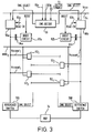
- Figure 3 shows an alternative and preferred arrangement which has two voltage boost circuits associated with each sector of the array.
- Figure 3 is a simplified schematic diagram of one sector of the array showing the -four sub-wordlines SWL1 to SWL4 associated with the main wordline MWL0 for the first sector of the array.
- the sub-wordline decode circuit 56 receives the address bits on address lines 66a and 66b and the SECTOR ENABLE bus 72 as for the circuit of Figure 2.
- the sub-wordline drivers 521 to 524 are supplied with respective gate voltages Vccxswl1 , or Vccxswl2 derived from the gate voltage Vccx on line 54.
- each sector of the array similarly has left and right hand side voltage boost circuits and associated boost capacitors.
- the gate voltage Vccx is selectively applied to the sub-wordline drivers via respective multiplexors 96a and 96b. These multiplexors 96a,96b receive the sector select signals SWL SELECT from the sector decode circuit 56 as in Figure 2.
- the multiplexors also receive the READ-3V signal on lines 93a,93b respectively.
- the BOOST signal is selectively applied to activate the boost circuits 92a,92b.
- the BOOST signal can be decoded (by means not shown in Figure 3) so that only the required boost circuit is active at any time.
- the READ-3V signal is applied to all the multiplexors of the array in common and serves to isolate Vccx from all the signals Vccxswl1, Vccxswl2 etc in order to minimise the boosted capacitance.
- This embodiment has the advantage that the load on Vccx line 54 is eliminated during boosting. Moreover, the boost time is reduced because the resistance of the multiplexor itself is no longer in the boost path: the boost capacitor is connected directly to the respective one of the Vccxswl1 , vccxswl2 etc nodes input to the sub-wordline driver.
- the boost scheme described with reference to Figure 3 needs to be further adapted to enable the boosting of the voltage supplied to the reference circuit 74 associated with a given sector.
- the scheme of Figure 3 only boosts the selected gate voltage Vccxswl1 or Vccxswl2 etc. within a sector the voltage Vccx is not boosted and hence the boost switch circuit 300 of Figure 1 cannot be used.
- reference switches 396 and 398 are provided for each side of the sector, connected between one of the respective gate voltages Vccxswl1 and Vccxswl2 and the reference circuit 74.
- one of the two reference switches 396 or 398 When a sector is enabled one of the two reference switches 396 or 398 will be enabled by the signal SWL SELECT under the control of the SWL decode circuit 56 such that the one of the respective gate voltages Vccxswl1 or Vccxswl2 which is boosted will be connected to the reference circuit 74.
- the voltage on the wordline is not required to be boosted (i.e. when the supply voltage Vcc is 5V) one of the reference switches 396 or 398 can still be enabled to supply the Vcc level on either Vccxswl1 or Vccxswl2 to the reference circuit 74.
- the sub-wordline drivers can be simple circuits.
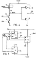
- An exemplary circuit for a sub-wordline driver is shown in Figure 4.
- the sub-wordline driver comprises a p-channel pull-up transistor 100 and first and second n-channel pull-down transistors 102 and 104 which are connected in series between the voltage Vccxswl supplied to the sub-wordline driver and a reference voltage Vss such as ground.
- the first and second series n-channel devices are not strong enough to pull down against the pull-up device 100 if its gate is at zero.
- the n-channel devices could be made stronger but would then use up more area, which is not desirable.
- the p-channel pull-up transistor 100 thus receives on its gate a signal NOTXPUP which serves to alter the strength of the pull-up device 100.
- the signal XPUP is held at 0V so that the pull-up transistor 100 is fully on. If desired, however the strength of the pull-up device could be changed during reading by altering the level of the signal XPUP as for programming.
- the first n-channel pull-down transistor 102 receives at its gate the address signal ADD from the sub-wordline decode circuit selecting that particular sub-wordline driver. This signal ADD is a CMOS level signal.
- the second n-channel pull-down transistor 104 receives on its gate the CMOS level from the main wordline driver and this is denoted MWL in Figure 4.
- An inverter comprising a p-channel device 106 and an n-channel device 108 connected in series between the voltage Vccxswl and the reference voltage Vss has an input NOTSWL on a node 110 between the p-channel pull-up transistor and the first n-channel pull-down transistor, the output of which is the sub-wordline itself SWL . It will be noted that in the circuit of Figure 4 the p-channel pull-up transistor 100 and p-channel transistor 106 of the inverter have their sources connected to Vccxswl .
- Each multiplexor comprises a level translator 302 and first and second transmission gates 304,306.
- the first transmission gate 304 is connected between Vcc and Vccxswl .
- the second transmission gate is connected between Vccx and Vccxswl .
- Vccxswl could be either Vccxswl1 , or Vccxswl2 here as appropriate.
- the level translator 302 has an input 305 and first and second outputs 307,308.
- the first output 307 controls the first transmission gate 304 and the second output 308 controls the second transmission gate 306.
- the first transmission gate 304 also receives an input from the SWL SELECT line.
- the second transmission gate 306 also receives as an input on line 305 the SWL SELECT signal inverted via an inverter 310.
- the multiplexor of Figure 5 operates so that when the signal SWL SELECT is high, the level translator 302 provides a low signal on output 308 and a high signal on output 307.
- the low signal on line 308 causes the second transmission gate 306 to connect the voltage Vccxswl to line Vccx .
- the high signal on output 307 causes the first transmission gate 304 to disconnect line Vccxswl from Vcc .
- the first transmission gate 304 connects node Vccxswl to the power supply voltage Vcc and the second transmission gate 306 disconnects line Vccxswl from Vccx .
- the voltages Vccxswl1, Vccxswl2 etc are held at Vcc. (Sub-wordlines in a deselected sector are held at OV by the sub-wordline driver circuit of Figure 4.)
- Vccxswl is at Vcc .
- the voltage on Vccx for example 12V during a program operation, is multiplexed onto Vccxswl .
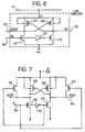
- Figure 6 is a transistor level diagram of the level translator 302 of Figure 5.
- the same circuit provides the level translators 312,314 in Figure 8 and 320,322 and 324 of Figure 9.
- the reference numerals in Figure 6 however correspond to those used in Figure 5.
- the level translator circuit comprises first and second input transistors 400,402.
- the first input transistor 400 receives the input signal 305 to the level translator and the second input transistor 402 receives an inverted version of that signal via an inverter 405.
- the level translator also includes first and second cross-coupled p-channel transistors 404,406. Complementary outputs from the level translator are taken from nodes 308 and 307 between each cross-coupled transistor and its respective input transistor.
- the level translator translates CMOS level signals on the input signal 305 to signals at the output nodes 307 and 308 the levels of which are determined by a voltage level HV supplying the level translator circuit.
- the translated signals can then be used to control circuits that are powered by non-CMOS level supplies, e.g. Vpp (12V) or boost levels.
- Vpp (12V) or boost levels e.g. Vpp (12V) or boost levels.
- the cross-coupied p-channel transistors 404 and 406 ensure zero dc current in the stable state.
- the advantage of the symmetrical circuit is to provide complementary translated circuit levels.
- the selected switch will have say 5V on node 902 and 5V on HVOUT node 904 which is connected to the reference circuit or, in the boosted case, 3V on node 902 and the boosted levels (5V) on HVOUT node 904 and hence the need for the level translator constituted by transistors 906,908,910,912 and inverter 914.
- the addition of two n-channel transistors 916,918 in parallel with the p-channel cross-coupled transistors is for the reason of passing low voltages from HV to HVOUT . This may be required when programming or characterising the reference cells.
- the boost short circuit 300 comprises first and second level translators 312,314 the outputs of which control a transmission gate 316.
- the transmission gate 316 is connected between Vccx and Vccr .
- the first and second level translators 312,314 receive an inverted version of the READ-3V signal via an inverter 317.
- the outputs on lines 318 and 320 respectively of the first and second level translators 312,314 go low and cause the transmission gate 316 to connect line Vccr to Vccx .
- the READ-3V signal is low, high outputs on lines 318 and 320 cause the transmission gate 316 to disconnect line Vccr from Vccx .
- Vccr is then driven from some other source such as Vcc .
- the multiplexor 96a,b comprises first, second and third level translators 320,322,324.
- the circuit also comprises first and second transmission gates 326,328.
- the first transmission gate 326 is connected between Vccx and Vccxswl .
- the second transmission gate 328 is connected between Vcc and Vccxswl .
- the first transmission gate 326 is controlled by the output from the first level translator 320 on line 330 and the output on line 332 from the second level translator 322.
- the second transmission gate 328 is controlled by the SWL SELECT signal on line 334 and the output from the third level translator 324 on line 336.
- the first and second level translators receive as their input the output 338 of a NAND gate 340.
- the NAND gate 340 receives as its inputs the inverse of the READ-3V signal on line 93 via an inverter 339, and the SWL SELECT signal.
- the third level translator 324 receives as an input the SWL SELECT signal on line 342.
- the SWL SELECT signal is low, indicating that the control circuit is inactive, the low signal on line 334 and the low signal on line 336 from the level translator 324 cause the transmission gate 328 to connect line Vccxswl to Vcc .
- the SWL SELECT signal is low, the output of the NAND gate on line 338 will be high, which forces high signals on lines 330 and 332. Therefore, the first transmission gate 326 disconnects line Vccxswl from Vccx .
- the transmission gate 328 disconnects line Vccxswl from Vcc .
- the line Vccxswl can therefore be connected to Vccx or boosted in dependence on the state of the READ-3V signal on line 93. If that signal is high, the high outputs on lines 330 and 332 will cause the transmission gate 326 to disconnect line Vccxswl from line Vccx to allow the node Vccxswl to be boosted. If the READ-3V signal on line 93 is low while the signal SWL SELECT is high however, low outputs on lines 330 and 332 will cause transmission gate 326 to connect line Vccxswl to Vccx .
- Figure 10 is a transistor level diagram of the transmission gate 306 shown in Figure 5.
- the same transmission gate structure is used as the transmission gate 316 in Figure 8 and the transmission gates 326,328 in Figure 9.
- the transmission gate comprises first and second input transistors 410,412 which are both p-channel transistors receiving the inputs 308,304 at their gates.
- the input transistors are connected in series between the line Vccx and line Vccxswl .
- Other transmission gates may be connected between different signal lines as appropriate, the circuit of Figure 10 illustrating the transmission gate 306 only.
- the transmission gate also includes complementary n-channel transistors 414,416 which are also connected in series between Vccx and Vccxswl .
- the pass gate mechanism is the two p-channel transistors 410,412 connected with their bulk connections connected to Vccx and Vccxswl . This is so that Vccx and Vccxswl can be at any two different voltage levels without any forward-bias condition on the source to bulk junctions that would discharge Vccx or Vccxswl .
- the two n-channel transistors 414,416 are used to bias the common node of the p-channel transistors 410,412 to whichever is the lower voltage of Vccx and Vccxswl , thus ensuring correct biasing.
- Each flash memory cell comprises a single floating gate transistor 4 having a control gate CG , a floating gate FG , a source S and a drain D .
- the source S of the floating gate transistor 4 is connected to an ARRAY GROUND signal on line 10.
- this line 10 can be at a ground voltage VGND or a high voltage Vpp .
- Voltage Vpp represents a programming potential (typically 12V) and voltage VGND represents device ground.
- the source voltage switch 14 is connected to the voltage Vpp via line 34 and the voltage VGND via line 36.
- the control gate CG of the floating gate transistor 4 is connected to the gate voltage switch 12 through the main wordline and sub-wordline decode circuitry discussed above and denoted schematically by block 3.
- the control gate receives the voltage Vccxswl .
- the gate voltage switch supplies voltage Vccx which can be derived from the power supply voltage Vcc , the programming voltage Vpp or VGND on lines 26,24 and 22 respectively.
- the switches 12 and 14 each receive a control signal ERASE on line 28 and additionally the gate voltage switch 12 receives a control signal program on line 30.
- the drain D of the floating gate transistor 4 is connected to the bit line BL which itself can be connected to the program load 32, a sense amplifier 29, or a floating connection FLOAT on line 17 through a bit line switch circuit 31.
- the flash memory has three primary modes of operation: program, erase and read. Each of these modes will be described hereinafter with reference to Figure 1. It will be understood by a person skilled in the art that several other modes of operation, such as program verify for example, also exist. However, the present description is by way of background illustration only and therefore only these three modes will be described.
- the program mode involves writing a "0" to a memory cell or group of memory cells
- the erase mode involves removing a "0" from any cell that has a "0” stored in it such that the cells all effectively store "1"s
- the read mode involves reading a cell to establish whether it is programmed or erased, i.e. contains either a "0" or a "1".
- the control signal PROGRAM on line 30 is set such that the gate voltage switch 12 is configured to connect the voltage Vpp on line 24 to the control gate CG of transistor 4 via word line 8.
- the source voltage switch 14 is configured to connect the voltage VGND on line 36 to the source of transistor 4 via the ARRAY GROUND signal line 10.
- the bit line switch 31 is set such that the bit line on line 6 is connected to the program load 32 by line 27.
- the program load 32 is such that a voltage of between 4 and 8V is on the drain D of the transistor 4 via the bit line 6.
- the negative charge increases the threshold voltage of the floating gate transistor making it less conductive.
- the amount of negative charge accumulated at the floating gate depends on several factors, including the duration for which the control signal PROGRAM is set, the voltages applied to the gate and drain terminals, and the thickness of the oxide separating the floating gate from the channel of the transistor. Furthermore, as the cell is programmed the accumulation of negative charge on the floating gate causes the electric field across the field oxide to reduce such that a point is reached where no more negative charge is attracted to the floating gate such that the threshold voltage of the floating gate transistor saturates to a limit. In this way, a "0" is written into the cell. Normally, several program pulses may be needed, each pulse being followed by a verify cycle.
- the control signal ERASE on line 28 is set such that the gate voltage switch 12 is configured to connect the voltage VGND on line 22 to the control gate CG of the transistor 4 via the word line 8, and such that the switch 14 is configured to connect the voltage Vpp on line 34 to the source S of the transistor 4 via the ARRAY GROUND line 10.
- the bit line switch 31 is set such that the bit line 6 is connected to the floating connection FLOAT on line 17 so that it floats. As the floating gate transistor is fabricated such that the source region in the substrate underlies the floating gate, any negative charge on the floating gate will be reduced. The amount of negative charge removed from the floating gate FG depends on the various factors as discussed hereinabove with reference to a program operation. The reduction of negative charge reduces the threshold voltage of the floating gate transistor making it more conductive. In this way the state of the cell is restored to "1". Normally, several erase pulses may be required, each erase pulse being followed by a verify cycle.
- the Vcc signal on line 26 is connected by the source voltage switch 12 to the control gate of the transistor 4 via the line Vccx and the word line 8. If the device is a 3V part, the supply voltage Vcc is disconnected from the signal Vccx , and hence the wordline WL 8, is boosted above Vcc by means not shown.
- the voltage VGND on line 36 is connected to the source of the transistor 4 via the ARRAY GROUND signal line 10.
- the bit line 6 is biased to approximately 1 volt during a read operation by means (discussed later) within the sense amplifying circuit.
- the current passed (or not) by the cell is compared with a reference current to detect the status of the cell.
Abstract
Description
- The present invention relates to an integrated circuit memory device with a voltage boost facility.
- Integrated circuit memory devices are made which can operate with different power supply voltages. For example, a typical memory chip can operate with a power supply voltage of 5V±10% or with a power supply voltage of 3.3V±0.3V. For an integrated circuit memory device which includes non-volatile single floating gate transistor memory cells which are to be programmed or erased, or read, it is necessary for certain read operations to provide a voltage of approximately 5V to the gates of the cells. A voltage of about 5V is sufficient to deliver enough cell current for reliable sensing in cells having an erase threshold voltage of about 3V which is the highest practical maximum in existing floating gate transistor cells in non-volatile memories. Where the power supply voltage is 5V, the necessary voltage required for reading can be -derived directly from the power supply itself. However, where the power supply voltage is nominally 3.3V, it is necessary to boost this voltage up to a value in excess of 4V and preferably about 5V for the required read operations. This can be done by a voltage boost circuit or a pump circuit. Voltage boost circuits are known and are not discussed in detail herein. They include a boot capacitor across which the output boosted voltage is provided. The boosted level is determined by the ratio of the boot capacitor to the amount of capacitance which is connected on the supply line on which the voltage is to be boosted. If this capacitance can be reduced, then the size of the boot capacitor can be reduced to maintain the ratio thus give the same boosted level. This gives an advantage in a reduction of chip area, time taken to boost the supply voltage, power and on-chip noise generated by the circuit.
- Pump circuits are also known and are not discussed further herein. Briefly, a pump circuit relies on several capacitively coupled stages, isolated by diodes, to progressively raise the voltage to the required level. These stages are driven by non-overlapping clocks. A reduction of the capacitance to be raised is also advantageous for these circuits.
- In an existing memory array, the power supply line to be boosted is connected to all the cells in a row of the memory and to the peripheral circuits for driving the wordlines. Thus, there is a significant amount of capacitance connected to the supply line when the supply voltage is boosted. The present invention seeks to reduce the capacitance connected to the power supply line when the supply voltage is boosted in order to overcome these problems.
- Random access memories (RAM) having so-called divided wordline (DWL) architectures are known, in which a wordline is divided into independently addressable sub-wordlines. This improves memory speed by avoiding long wordlines and the associated larger resistances and capacitances. It would be desirable to use DWL architecture in so-called flash memories, that is memories made up of electrically erasable and programmable single floating gate transistor cells, to utilise its speed advantages. However, in these memories, problems arise in routing different voltage levels to the gates of the cells and keeping sub-wordline drive circuits relatively simple and hence small. It will be appreciated that there is a trade-off between improvement in speed using a DWL architecture and area consumed by the required sub-wordline drive circuits. Problems associated with routing different voltages to the gates of the cells are compounded when the voltage supply level has to be increased by pumping or boosting. Furthermore, sub-wordline drive circuits increase the capacitance on the voltage line to be boosted.
- According to the present invention there is provided an integrated circuit memory device comprising:
- a memory array comprising a plurality of memory cells arranged in rows and columns, the cells in a row of a sector being arranged in sectors with the cells in each sector being connected to a common respective sub-wordline and cells in a column being connected to a common bit line;
- a plurality of sub-wordline drive circuits associated respectively with said sub-wordlines and connected to supply a cell voltage to their associated sub-wordline;
- voltage raising circuitry for raising a power supply voltage connected on a memory voltage supply line to said cell voltage;
- row addressing circuitry for selecting one of the sub-wordlines in one of said sectors; and
- control circuitry for selectively disconnecting from said memory voltage supply line sub-wordline drive circuits associated with sub-wordlines in non-selected sectors.
- Normally, each sector will contain a plurality of sub-wordlines, and one or more groups of sub-wordline drive circuits.
- Preferably the control circuitry comprises a plurality of voltage control switches, each voltage control switch being associated with a group of sub-wordline drive circuits for applying said cell voltage to a group of sub-wordline drive circuits when a sub-wordline associated with a sub-wordline drive circuit in that group is selected.
- Each voltage control switch can be made responsive to a SECTOR ENABLE signal so that it can be disabled when the sub-wordline drive circuit or sub-wordline drive circuits associated with that voltage switch are not selected.
- When disabled, the voltage control switch can connect the group of sub-wordline drive circuits to the power supply voltage.
- The integrated circuit memory device can include a plurality of main wordlines extending in the row direction, each main wordline being connected to a plurality of sub-wordline drive circuits in the column direction.
- In that case, the row addressing circuitry comprises a main wordline decode circuit for selecting one of said plurality of main wordlines and a sub-wordline decode circuit for selecting a group of said sub-wordline drive circuits.
- There is preferably a sub-wordline decode circuit associated with each of said sectors.
- In a particularly advantageous embodiment, the sub-wordline drive circuits connected to each main wordline and extending in the column direction can be arranged in an interleaved fashion with sub-wordline drive circuits associated with alternate sub-wordlines being located on opposite sides of said sector of cells. This relaxes the pitch of the sub-wordline drive circuits and therefore eases layout problems in fitting in the required number of sub-wordline drive circuits. In this architecture, there can be one voltage control switch associated with the group of sub-wordline drive circuits on each side of each sector of cells. This arrangement also further reduces the capacitance connected to the supply line.
- In one embodiment, the voltage raising circuitry comprises a single voltage boost circuit and a boost capacitor connected between the voltage boost circuit and a common memory voltage supply line. When the voltage boost circuit is active, the boost capacitor increases the voltage on said common memory voltage supply line above the power supply voltage. In this embodiment the boost capacitor extends across the width of the memory array to minimise RC delays on the boosted node.
- In an alternative embodiment, the voltage raising circuitry comprises a plurality of voltage boost circuits and associated boost capacitors, wherein each sector of cells has associated therewith at least one voltage boost circuit and a boost capacitor. In that case, each boost capacitor is connected between its voltage boost circuit and a group of sub-wordline drive circuits of said sector. It will be appreciated that in this embodiment, the single capacitor extending widthwise of the array in the previous embodiment has been replaced by a plurality of individual capacitors, appropriately resized. The control circuitry is operative to connect the power supply voltage to the boost capacitor of selected sectors thereby to permit said boost capacitor to supply said cell voltage to a sub-wordline drive circuit of a selected sub-wordline.
- In the previous embodiment, the capacitance of all the control circuitry is connected to the supply line during boosting and this can be a large proportion of the total capacitance. This is eliminated in this alternative embodiment.
- Sector switches can also be provided for selectively applying a boosted power supply voltage to reference circuits which are associated with sense circuitry of each sector.
- The provision of the control switches and sector switches enables the capacitance associated with the voltage boost circuit to be minimised by connecting to the voltage boost circuit only those elements which are intended to receive the boosted power supply voltage and disconnecting other elements from the line on which the voltage is to be boosted. In the aforementioned alternative embodiment there is a further improvement in reducing capacitance by not having all the control circuitry connected to the line to be boosted.
- Another advantage of the so-called DWL architecture when applied to flash memories arises during programming of the memory, when the gates of all cells connected to a wordline are taken to the programming voltage of 12V. The effect of this is to increase the threshold voltages of erased cells. In a DWL architecture, sub-wordlines are only active on a per sector basis and therefore cells are subject to far less stress throughout the lifetime of the part. In a non-DWL architecture, means have to be provided to relieve this stress in non-selected sectors.
- For a better understanding of the present invention and to show how the same may be carried into effect reference will now be made by way of example to the accompanying drawings in which:
- Figure 1 is a block diagram showing the main elements of a flash memory circuit;
- Figure 2 is a schematic showing one sector of the array in a first embodiment;
- Figure 3 is a schematic showing one sector of the array in a second embodiment;
- Figure 4 is a transistor level diagram of a sub-wordline driver;
- Figure 5 is a block diagram of a control switch for the first embodiment of the invention;
- Figure 6 is a transistor level diagram of level translators used in the circuits of Figures 5, 8 and 9;
- Figure 7 is a transistor level diagram of a sector reference switch;
- Figure 8 is a block diagram of a boost short circuit switch;
- Figure 9 is a block diagram of a control switch for the second embodiment of the invention;
- Figure 10 is a transistor diagram of transmission gates used in the circuits of Figures 5, 8 and 9; and
- Figure 11 is a schematic diagram illustrating operation of a flash memory cell.
- Figure 1 is a schematic diagram of a flash memory array. The array consists of a plurality of memory cells extending in rows and columns. The array comprises a plurality n of main wordlines MWL0 to MWLn. Each main wordline extends along the full width of the memory array in the row direction. The memory array also comprises a plurality of bit lines. The array is divided into sectors, each sector including a plurality of columns of cells, each column of cells being connected to a respective bit line. Each sector has a plurality p of columns and a corresponding plurality p of bit lines which are denoted BL0 to BLp for the
first sector SECTOR 1 of the array shown in Figure 1. A sub-wordline extends along the width of one sector and is connected to all cells in a row of the sector, in this case p cells. There is a plurality of sub-wordlines extending across the array equal to the number of sectors, each sub-wordline being addressable independently of other sub-wordlines in the same row. This is a so-called divided wordline (DWL) architecture. In addition, in the array of Figure 1, each main wordline is associated with four sub-wordlines defining respectively four rows of the sector. These are denoted SWL1, SWL2, SWL3 and SWL4 for thefirst sector SECTOR 1 shown in Figure 1. Thus, the main wordline runs on a pitch of four cells, that is there are four cells column wise between each main wordline. The pitch of the main wordline is not critical to the present invention and any suitable pitch could be selected, subject to limitations of the process used to manufacture the memory device. In particular, pitches of 2,4,8,16 are advantageous for reasons of decoding as will be evident from the following description. Each main wordline MWL0 to MWLn has associated with it amain wordline driver 50₀ to 50n which is a simple CMOS logic driver. This need drive only a straightforward CMOS level onto the main wordline. Each sub-wordline has associated with it a respective sub-wordline driver. These sub-wordline drivers are denoted 52₁,52₂,52₃ and 52₄ for the sub-wordlines SWL1 to SWL4 respectively. Each of thesesub-wordline drivers 52₁ to 52₄ receives a CMOS logic level signal online 53 from their associatedmain wordline driver 50₀ to 50n when that main wordline driver is driven. Thesub-wordline drivers 52₁ to 52₄ also each receive a respective gate voltage signal Vccxswl₁ or Vccxswl₂ which is derived via multiplexors (not shown in Figure 1) from a common supply voltage Vccx online 54 from agate voltage switch 12. Eachsub-wordline driver 52₁ to 52₄ can be selected through a sub-wordlinedriver decode circuit 56. There is asub-wordline decode circuit 56 associated with each sector of the array. The mainwordline drivers 50₀ to 50n can be individually activated via a mainwordline decode circuit 58. The mainwordline decode circuit 58 receives a main wordline address 60. Each of thesub-wordline decode circuits 56 receives asub-wordline address 62, thesub-wordline address 62 and the main wordline address 60 being derived from arow address 64. In the case where there are four sub-wordlines associated with each main wordline in the column direction, the sub-wordline address consists of two bits. These two bits are the two least significant bits of the row address. These are supplied to eachsub-wordline decode circuit 56 on a twobit bus 66. - Each sub-wordline drive circuit thus receives address signals ADD from the
sub-wordline decode circuit 56, and mainwordline MWL signals. It will be appreciated that the mainwordline MWL signals extend widthwise of the array and the ADD signals extend the full depth of the array. - Each sector of the array has associated with it a
column decode circuit 68 to which the bit lines BL0 to BLp are connected. The column decodecircuits 68 are responsive to acolumn address 70 to connect selected ones of the bit lines BL0 to BLp to each of a plurality ofsense amplifiers 29 associated with each sector. This embodiment is an eight bit wide memory and there are eight sense amplifiers associated with each sector. Thus, eight bit lines are selected from the sector via thecolumn decode circuit 68 in response to thecolumn address 70, the bits from these cells are read by thesense amplifiers 29 and then supplied to an eight bit data bus 23. Thesub-wordline decode circuit 56 is responsive to a sector enable code onbus 72 to generate a sector select signal SWL SELECT to enable that particular sector. The column decodecircuits 68 are responsive to the sector select signal SWL SELECT so that those circuits of non-selected sectors are disabled. Thesense amplifiers 29 in each sector each have associated with them areference circuit 74 for supplying a reference current which is used during sensing. Thereference circuit 74 is connected to a voltage Vccr online 76 through asector switch 78. Thatsector switch 78 is again responsive to the sector select signal SWL SELECT. As will readily be appreciated, thereference circuit 74 supplies its reference current to each of thesense amplifiers 29 in the respective sector. The bit lines BL0 to BLp can also selectively be connected through thecolumn decode circuit 68 to aprogram load 32 in each sector for the purposes of programming the cells of the array. - The gate voltage Vccx output from the
gate voltage switch 12 can have a plurality of different voltage levels as discussed in more detail in the following. In particular, for reading data from the cells a voltage of about 5V is required online 54. Where the memory chip is a 5V part, that is with a power supply of 5V±10%, the voltage Vccx can in that case be derived from the supply voltage itself. However, where the memory chip is a 3V part, that is with a nominal supply voltage of 3.3V±.3V it is necessary to boost the voltage online 54 up to a level of about 5V for reading. This is done via avoltage boost circuit 80 which includes as is known aboot capacitor 82 for providing the boosted voltage. Voltage boost circuits are known in the art and so further information will not be given herein. The voltage boost circuit is able to boost a supply voltage of 3.3V±.3V to a level of about 5V adequate for reading. A particularly suitable voltage boost circuit is described in our copending Application No. (Page White & Farrer Ref. 76218), the contents of which are herein incorporated by reference. - The
voltage boost circuit 80 is activated in response to a boost signal BOOST online 84. - The voltage level which can be achieved on
line 54 is determined by the ratio of the size of theboot capacitor 82 to the amount of capacitance connected toline 54, the sub-wordline gate voltage signal line Vccxswl and the sub-wordline itself, i.e. the total capacitance which is boosted. If this boosted capacitance can be decreased, then the size of theboot capacitor 82 may be reduced for a given boosted voltage level online 54. This gives advantages of a saving in chip area, a reduction in the time taken to boost the voltage level and reduction in power and on-chip noise generated by the boost circuit. - This is achieved with the circuits described herein by minimising the number of memory cells and sub-wordline drive circuits connected to line 54 so that the capacitance to be boosted is kept to a minimum when the
voltage boost circuit 80 is active. - One way in which this can be achieved is illustrated by the circuit of Figure 2, which shows in more detail the first sector of the array and in particular the four sub-wordlines SWL1 to SWL4 associated with the main wordline MWL0. Each sub-wordline has a plurality p of flash memory cells FC0 to FCp connected to it. For reasons of clarity these are shown only for the sub-wordline SWL1 in Figure 2. As described in more detail in the following, each flash cell FC comprises a floating gate transistor having its gate connected to the sub-wordline, its drain connected to the bit line BL0 to BLp respectively and its source connected to a voltage on
line 86 from a source voltage switch 14. There are associated with each sector two control switches ormultiplexors multiplexor 88a receives the voltage Vccx online 54 and supplies that voltage, when activated, to thesub-wordline drivers line 54 and, when activated, supplies that voltage to thesub-wordline drivers multiplexors bus 72 and whichever one of the bits of the twobit bus 66 is used to select between right and left hand sides of the sector. The twobit bus 66 comprises twoaddress lines first address line 66a carries the bit used to select between the group of sub-wordline drive circuits on either the right or the left hand sides of the sector. Thesecond address line 66b carries the bit used to select between one of the two sub-wordline drivers on the side of the sector selected by thefirst address line 66a. Themultiplexor 88a is connected to receive the signal SWL SELECT online 87a and the multiplexor 88b is also connected to receive an SWL SELECT signal online 87b. It will be appreciated that when themultiplexor 88a is selected the multiplexor 88b and the other multiplexor of the array are not selected. This ensures that when themultiplexor 88a is active for selection of the group of sub-wordline drivers on the left hand side of the sector, themultiplexor 88b is inactive. It will be clear that thesub-wordline decode circuit 56 is arranged to decode the address signals onlines address line 66a in one state, the sub-wordline drivers on the same side of the sector are selected. The address lines ADD from thesub-wordline decode circuit 56 to the sub-wordline drivers are omitted from Figure 2 for the sake of clarity. - The
multiplexors - In the circuit of Figure 2, the
voltage boost circuit 80 is activated in response to the signal BOOST online 84 which is applied for a 3V part when the voltage Vccx is to be boosted from 3.3V±.3V to about 5V. - Reverting to Figure 1, if the power supply voltage Vccx requires boosting for reading of the memory array, the voltage Vccr must also be boosted in the
reference circuit 74 for thesense amplifiers 29 of the selected sector in order to bias the reference so that programmed and erased cells can be sensed. This is because a functional cell in thereference circuit 74 is used to generate the reference and hence must be biased in the same condition as the cells in the array. A similar principle can be used to route the boosted voltage Vccr only to the selected sector by the use of the sector reference switches 78, which selectively connect the voltage Vccr to thereference circuits 74 for enabled sectors in response to the SWL SELECT signal online 87a derived from thesector decode circuit 56. This has the advantage of routing the boosted voltage only to required reference circuits (reducing the stress on reference cells in reference circuits of non-selected sectors) and reduces the capacitance online 76, disabled sectors being held at OV, effectively disconnected fromline 76. - In order to boost Vccr, Vccr is shorted to Vccx during 3V read cycles by a boost
short circuit 300 responsive to a READ-3V signal as described in more detail later. The READ-3V signal is active throughout read cycles when the part is configured to have a power supply voltage of 3.3V, i.e. when boosting is likely to be required. When the signal Vccr is not required to be boosted, the boostshort circuit 300 is disabled. - In the circuit of Figure 2, there is a common
voltage boost circuit 80 andcommon boot capacitor 82. Figure 3 shows an alternative and preferred arrangement which has two voltage boost circuits associated with each sector of the array. - Figure 3 is a simplified schematic diagram of one sector of the array showing the -four sub-wordlines SWL1 to SWL4 associated with the main wordline MWL0 for the first sector of the array. The
sub-wordline decode circuit 56 receives the address bits onaddress lines SECTOR ENABLE bus 72 as for the circuit of Figure 2. Thesub-wordline drivers 52₁ to 52₄ are supplied with respective gate voltages Vccxswl₁, or Vccxswl₂ derived from the gate voltage Vccx online 54. There is avoltage boost circuit 92a with aboot capacitor 94a associated with the left hand side of the sector. Similarly, there is avoltage boost circuit 92b and aboot capacitor 94b associated with the right hand side of the sector. Each sector of the array similarly has left and right hand side voltage boost circuits and associated boost capacitors. The gate voltage Vccx is selectively applied to the sub-wordline drivers viarespective multiplexors multiplexors sector decode circuit 56 as in Figure 2. The multiplexors also receive the READ-3V signal onlines boost circuits - This embodiment has the advantage that the load on
Vccx line 54 is eliminated during boosting. Moreover, the boost time is reduced because the resistance of the multiplexor itself is no longer in the boost path: the boost capacitor is connected directly to the respective one of the Vccxswl₁, vccxswl₂ etc nodes input to the sub-wordline driver. - Operation of the
multiplexors sub-wordline decode circuit 56 to thesub-wordline drivers 52₁ to 52₄ have been omitted for reasons of clarity. - The boost scheme described with reference to Figure 3 needs to be further adapted to enable the boosting of the voltage supplied to the
reference circuit 74 associated with a given sector. As the scheme of Figure 3 only boosts the selected gate voltage Vccxswl₁ or Vccxswl₂ etc. within a sector the voltage Vccx is not boosted and hence theboost switch circuit 300 of Figure 1 cannot be used. Referring to Figure 3reference switches reference circuit 74. When a sector is enabled one of the tworeference switches SWL decode circuit 56 such that the one of the respective gate voltages Vccxswl₁ or Vccxswl₂ which is boosted will be connected to thereference circuit 74. When the voltage on the wordline is not required to be boosted (i.e. when the supply voltage Vcc is 5V) one of the reference switches 396 or 398 can still be enabled to supply the Vcc level on either Vccxswl₁ or Vccxswl₂ to thereference circuit 74. - Another advantage of the circuits described above is that the sub-wordline drivers can be simple circuits. An exemplary circuit for a sub-wordline driver is shown in Figure 4. The sub-wordline driver comprises a p-channel pull-up
transistor 100 and first and second n-channel pull-downtransistors - During programming cycles with 12V on any one of the signals Vccxswl₁, Vccxswl₂ etc the first and second series n-channel devices are not strong enough to pull down against the pull-up
device 100 if its gate is at zero. The n-channel devices could be made stronger but would then use up more area, which is not desirable. The p-channel pull-uptransistor 100 thus receives on its gate a signal NOTXPUP which serves to alter the strength of the pull-updevice 100. For reading, the signal XPUP is held at 0V so that the pull-uptransistor 100 is fully on. If desired, however the strength of the pull-up device could be changed during reading by altering the level of the signal XPUP as for programming. This is because a 'sneak' path exists through the p-channel transistor 100 of the selected sub-wordline driver which slowly discharges the boosted capacitance. Reducing the strength of this pull-up device in turn reduces the rate of this discharge. The first n-channel pull-down transistor 102 receives at its gate the address signal ADD from the sub-wordline decode circuit selecting that particular sub-wordline driver. This signal ADD is a CMOS level signal. The second n-channel pull-down transistor 104 receives on its gate the CMOS level from the main wordline driver and this is denoted MWL in Figure 4. An inverter comprising a p-channel device 106 and an n-channel device 108 connected in series between the voltage Vccxswl and the reference voltage Vss has an input NOTSWL on anode 110 between the p-channel pull-up transistor and the first n-channel pull-down transistor, the output of which is the sub-wordline itself SWL. It will be noted that in the circuit of Figure 4 the p-channel pull-uptransistor 100 and p-channel transistor 106 of the inverter have their sources connected to Vccxswl. This is so that theinput node 110 to the inverter is pulled up to Vccxswl and so fully turn off the p-channel transistor 106 in the sub-wordline drivers of unselected sub-wordlines. Otherwise the boosted voltage will be severely degraded. - Reference will now be made to Figure 5 to describe the
multiplexors level translator 302 and first and second transmission gates 304,306. Thefirst transmission gate 304 is connected between Vcc and Vccxswl. The second transmission gate is connected between Vccx and Vccxswl. Vccxswl could be either Vccxswl₁, or Vccxswl₂ here as appropriate. Thelevel translator 302 has aninput 305 and first and second outputs 307,308. Thefirst output 307 controls thefirst transmission gate 304 and thesecond output 308 controls thesecond transmission gate 306. Thefirst transmission gate 304 also receives an input from the SWL SELECT line. Thesecond transmission gate 306 also receives as an input online 305 the SWL SELECT signal inverted via aninverter 310. The multiplexor of Figure 5 operates so that when the signal SWL SELECT is high, thelevel translator 302 provides a low signal onoutput 308 and a high signal onoutput 307. The low signal online 308 causes thesecond transmission gate 306 to connect the voltage Vccxswl to line Vccx. The high signal onoutput 307 causes thefirst transmission gate 304 to disconnect line Vccxswl from Vcc. In contrast, when the signal SWL SELECT goes low, thefirst transmission gate 304 connects node Vccxswl to the power supply voltage Vcc and thesecond transmission gate 306 disconnects line Vccxswl from Vccx. Thus, for non-activated control switches the voltages Vccxswl₁, Vccxswl₂ etc are held at Vcc. (Sub-wordlines in a deselected sector are held at OV by the sub-wordline driver circuit of Figure 4.) - The following truth table for Figure 5 demonstrates this clearly.
SWL SELECT Vccxswl 0 Vcc 1 Vccx (Boost) - Thus, if a sector is not selected, Vccxswl is at Vcc. In any other cycle the voltage on Vccx, for example 12V during a program operation, is multiplexed onto Vccxswl.
- Figure 6 is a transistor level diagram of the
level translator 302 of Figure 5. The same circuit provides the level translators 312,314 in Figure 8 and 320,322 and 324 of Figure 9. The reference numerals in Figure 6 however correspond to those used in Figure 5. The level translator circuit comprises first and second input transistors 400,402. Thefirst input transistor 400 receives theinput signal 305 to the level translator and thesecond input transistor 402 receives an inverted version of that signal via aninverter 405. The level translator also includes first and second cross-coupled p-channel transistors 404,406. Complementary outputs from the level translator are taken fromnodes input signal 305 to signals at theoutput nodes channel transistors - Reference will now be made to Figure 7 to describe operation of a
sector reference switch 78. This circuit routes the reference level to the reference circuits and is a small variation on the level translator of Figure 6. If there are four reference circuits then three of the four switches will have 0V on theinput node 902 which is connected to the sector select signal SWL SELECT and so theoutput node 904 HVOUT will also be OV and so the reference circuits will be disabled. The selected switch will have say 5V onnode 902 and 5V onHVOUT node 904 which is connected to the reference circuit or, in the boosted case, 3V onnode 902 and the boosted levels (5V) onHVOUT node 904 and hence the need for the level translator constituted by transistors 906,908,910,912 andinverter 914. The addition of two n-channel transistors 916,918 in parallel with the p-channel cross-coupled transistors is for the reason of passing low voltages from HV to HVOUT. This may be required when programming or characterising the reference cells. - Reference will now be made to Figure 8 to describe the boost
short circuit 300. The boostshort circuit 300 comprises first and second level translators 312,314 the outputs of which control atransmission gate 316. Thetransmission gate 316 is connected between Vccx and Vccr. The first and second level translators 312,314 receive an inverted version of the READ-3V signal via aninverter 317. When the READ-3V signal is high, the outputs onlines transmission gate 316 to connect line Vccr to Vccx. When the READ-3V signal is low, high outputs onlines transmission gate 316 to disconnect line Vccr from Vccx. Vccr is then driven from some other source such as Vcc. - Reference will now be made to Figure 9 to describe the
multiplexors multiplexor 96a,b comprises first, second and third level translators 320,322,324. The circuit also comprises first and second transmission gates 326,328. Thefirst transmission gate 326 is connected between Vccx and Vccxswl. Thesecond transmission gate 328 is connected between Vcc and Vccxswl. Thefirst transmission gate 326 is controlled by the output from thefirst level translator 320 online 330 and the output online 332 from thesecond level translator 322. Thesecond transmission gate 328 is controlled by the SWL SELECT signal online 334 and the output from thethird level translator 324 online 336. The first and second level translators receive as their input theoutput 338 of aNAND gate 340. TheNAND gate 340 receives as its inputs the inverse of the READ-3V signal online 93 via aninverter 339, and the SWL SELECT signal. Thethird level translator 324 receives as an input the SWL SELECT signal online 342. When the SWL SELECT signal is low, indicating that the control circuit is inactive, the low signal online 334 and the low signal online 336 from thelevel translator 324 cause thetransmission gate 328 to connect line Vccxswl to Vcc. When the SWL SELECT signal is low, the output of the NAND gate online 338 will be high, which forces high signals onlines first transmission gate 326 disconnects line Vccxswl from Vccx. - When the signal SWL SELECT is high, the
transmission gate 328 disconnects line Vccxswl from Vcc. The line Vccxswl can therefore be connected to Vccx or boosted in dependence on the state of the READ-3V signal online 93. If that signal is high, the high outputs onlines transmission gate 326 to disconnect line Vccxswl from line Vccx to allow the node Vccxswl to be boosted. If the READ-3V signal online 93 is low while the signal SWL SELECT is high however, low outputs onlines transmission gate 326 to connect line Vccxswl to Vccx. - The following table indicates the operation of the circuit of Figure 9.
SELECT READ-3V Vccx_SWL 0 0 VCC 0 1 VCC 1 0 Vccx 1 1 (BOOST) - Thus, operation is the same as for Figure 5 except if READ_3V is active (HIGH), then in the selected sector Vccxswl is isolated and boosted. For other cycles such as program the 12V on Vccx is-multiplexed onto Vccxswl as above.
- Figure 10 is a transistor level diagram of the
transmission gate 306 shown in Figure 5. The same transmission gate structure is used as thetransmission gate 316 in Figure 8 and the transmission gates 326,328 in Figure 9. The transmission gate comprises first and second input transistors 410,412 which are both p-channel transistors receiving the inputs 308,304 at their gates. The input transistors are connected in series between the line Vccx and line Vccxswl. Other transmission gates may be connected between different signal lines as appropriate, the circuit of Figure 10 illustrating thetransmission gate 306 only. The transmission gate also includes complementary n-channel transistors 414,416 which are also connected in series between Vccx and Vccxswl. - The way this works is that the pass gate mechanism is the two p-channel transistors 410,412 connected with their bulk connections connected to Vccx and Vccxswl. This is so that Vccx and Vccxswl can be at any two different voltage levels without any forward-bias condition on the source to bulk junctions that would discharge Vccx or Vccxswl. The two n-channel transistors 414,416 are used to bias the common node of the p-channel transistors 410,412 to whichever is the lower voltage of Vccx and Vccxswl, thus ensuring correct biasing.
- Reference will finally be made to Figure 11 to describe the basic operation of each flash memory cell FC. Each flash memory cell comprises a single floating gate transistor 4 having a control gate CG, a floating gate FG, a source S and a drain D. The source S of the floating gate transistor 4 is connected to an ARRAY GROUND signal on
line 10. Through the source voltage switch 14 thisline 10 can be at a ground voltage VGND or a high voltage Vpp. Voltage Vpp represents a programming potential (typically 12V) and voltage VGND represents device ground. The source voltage switch 14 is connected to the voltage Vpp vialine 34 and the voltage VGND vialine 36. The control gate CG of the floating gate transistor 4 is connected to thegate voltage switch 12 through the main wordline and sub-wordline decode circuitry discussed above and denoted schematically by block 3. Thus, the control gate receives the voltage Vccxswl. The gate voltage switch supplies voltage Vccx which can be derived from the power supply voltage Vcc, the programming voltage Vpp or VGND onlines switches 12 and 14 each receive a control signal ERASE online 28 and additionally thegate voltage switch 12 receives a control signal program online 30. The drain D of the floating gate transistor 4 is connected to the bit line BL which itself can be connected to theprogram load 32, asense amplifier 29, or a floating connection FLOAT on line 17 through a bitline switch circuit 31. - The flash memory has three primary modes of operation: program, erase and read. Each of these modes will be described hereinafter with reference to Figure 1. It will be understood by a person skilled in the art that several other modes of operation, such as program verify for example, also exist. However, the present description is by way of background illustration only and therefore only these three modes will be described. The program mode involves writing a "0" to a memory cell or group of memory cells, the erase mode involves removing a "0" from any cell that has a "0" stored in it such that the cells all effectively store "1"s, and the read mode involves reading a cell to establish whether it is programmed or erased, i.e. contains either a "0" or a "1".
- During a program mode, the control signal PROGRAM on
line 30 is set such that thegate voltage switch 12 is configured to connect the voltage Vpp on line 24 to the control gate CG of transistor 4 viaword line 8. As the control signal ERASE online 28 is not set the source voltage switch 14 is configured to connect the voltage VGND online 36 to the source of transistor 4 via the ARRAYGROUND signal line 10. Thebit line switch 31 is set such that the bit line online 6 is connected to theprogram load 32 byline 27. Theprogram load 32 is such that a voltage of between 4 and 8V is on the drain D of the transistor 4 via thebit line 6. As a result of these signals applied to the transistor 4 the floating gate FG becomes negatively charged. The negative charge increases the threshold voltage of the floating gate transistor making it less conductive. The amount of negative charge accumulated at the floating gate depends on several factors, including the duration for which the control signal PROGRAM is set, the voltages applied to the gate and drain terminals, and the thickness of the oxide separating the floating gate from the channel of the transistor. Furthermore, as the cell is programmed the accumulation of negative charge on the floating gate causes the electric field across the field oxide to reduce such that a point is reached where no more negative charge is attracted to the floating gate such that the threshold voltage of the floating gate transistor saturates to a limit. In this way, a "0" is written into the cell. Normally, several program pulses may be needed, each pulse being followed by a verify cycle. - During an erase mode, the control signal ERASE on
line 28 is set such that thegate voltage switch 12 is configured to connect the voltage VGND online 22 to the control gate CG of the transistor 4 via theword line 8, and such that the switch 14 is configured to connect the voltage Vpp online 34 to the source S of the transistor 4 via theARRAY GROUND line 10. Thebit line switch 31 is set such that thebit line 6 is connected to the floating connection FLOAT on line 17 so that it floats. As the floating gate transistor is fabricated such that the source region in the substrate underlies the floating gate, any negative charge on the floating gate will be reduced. The amount of negative charge removed from the floating gate FG depends on the various factors as discussed hereinabove with reference to a program operation. The reduction of negative charge reduces the threshold voltage of the floating gate transistor making it more conductive. In this way the state of the cell is restored to "1". Normally, several erase pulses may be required, each erase pulse being followed by a verify cycle. - During a read mode, neither the control signal ERASE on
line 28 nor the control signal PROGRAM online 30 are set, but the READ signal online 21 is set. The Vcc signal online 26 is connected by thesource voltage switch 12 to the control gate of the transistor 4 via the line Vccx and theword line 8. If the device is a 3V part, the supply voltage Vcc is disconnected from the signal Vccx, and hence thewordline WL 8, is boosted above Vcc by means not shown. The voltage VGND online 36 is connected to the source of the transistor 4 via the ARRAYGROUND signal line 10. Thebit line 6 is biased to approximately 1 volt during a read operation by means (discussed later) within the sense amplifying circuit. During a read operation, for an erased cell (with "1" stored in it) the conductivity of the cell is such that current passes through the cell when the bit line is connected for sensing. For a programmed cell (with a "0" stored in it) substantially no current is passed by the cell. - The current passed (or not) by the cell is compared with a reference current to detect the status of the cell.
Claims (16)
- An integrated circuit memory device comprising:a memory array comprising a plurality of memory cells arranged in rows and columns, the cells in a row of a sector being arranged in sectors with the cells in each sector being connected to a common respective sub-wordline and cells in a column being connected to a common bit line;a plurality of sub-wordline drive circuits associated respectively with said sub-wordlines and connected to supply a cell voltage to their associated sub-wordline;voltage raising circuitry for raising a power supply voltage connected on a memory voltage supply line to said cell voltage;row addressing circuitry for selecting one of the sub-wordlines in one of said sectors; andcontrol circuitry for selectively disconnecting from said memory voltage supply line sub-wordline drive circuits associated with sub-wordlines in non-selected sectors.
- An integrated circuit memory device according to claim 1 wherein said control circuitry comprises a plurality of voltage control switches, each voltage control switch being associated with a group of sub-wordline drive circuits for applying said cell voltage to a group of sub-wordline drive circuits when a sub-wordline associated with a sub-wordline drive circuit in that group is selected.
- An integrated circuit memory device according to claim 2 wherein each voltage control switch is responsive to a sector enable signal so that it can be disabled when the sub-wordline drive circuits associated with that voltage switch are not selected.
- An integrated circuit memory device according to any preceding claim which comprises a plurality of main wordlines extending in the row direction, each main wordline being connected to a plurality of sub-wordline drive circuits in the column direction.
- An integrated circuit memory device according to claim 4 wherein said row addressing circuitry comprises a main wordline decode circuit for selecting one of said plurality of main wordlines and a sub-wordline decode circuit for selecting one of said sub-wordline drive circuits connected to said selected main wordline.
- An integrated circuit memory device according to claim 5 which comprises a plurality of said sub-wordline decode circuits associated respectively with said sectors of cells.
- An integrated circuit memory device according to claim 4, 5, or 6 wherein the sub-wordline drive circuit connected to each main wordline and extending in the column direction are arranged in an interleaved fashion with sub-wordline drive circuits associated with alternate sub-wordlines being located on opposite sides of said sector of cells.
- An integrated circuit memory device according to claim 7 when appended to claim 2 wherein there is a voltage control switch associated with the sub-wordline drive circuits on each side of said sector of cells.
- An integrated circuit memory device according to any preceding claim wherein said voltage raising circuitry comprises a voltage boost circuit and a boost capacitor connected between said voltage boost circuit and the common memory voltage supply line which is connected between said power supply voltage terminal and said control circuitry so that when said voltage boost circuit is active, the boost capacitor increases the voltage on said memory voltage supply line above the power supply voltage.
- An integrated circuit memory device according to any of claims 1 to 8 wherein said voltage raising circuitry comprises a plurality of voltage boost circuits and associated boost capacitors, wherein each sector of cells has associated therewith at least one voltage boost circuit and a boost capacitor, said boost capacitor being connected between its voltage boost circuit and a group of sub-wordline drive circuits of said sector, said control circuitry being operative to connect the power supply voltage to said boost capacitor thereby to permit said boost capacitor of selected sectors to supply said cell voltage to a sub-wordline drive circuit of a selected sub-wordline.
- An integrated circuit memory device according to any preceding claim wherein the bit lines associated with each sector of cells are connected to a respective column decode circuit for that sector, said column decode circuit being activated in response to a sector enable signal.
- An integrated circuit memory device according to claim 11 which comprises for each sector a plurality of sense amplifiers, the column decode circuit for each sector being responsive to a column address to selectively connect bit lines of the sector to said sense amplifiers, said sense amplifiers receiving a reference current from a reference circuit associated with the sector.
- An integrated circuit memory device according to claim 12 which comprises a plurality of sector switches associated with each sector for selectively applying a boosted power supply voltage to said reference circuits.
- An integrated circuit memory device according to any preceding claim wherein each sub-wordline drive circuit comprises a pull-up device and a pull-down device connected in series between said cell voltage and a reference voltage, and an inverter connected between a node between said pull-up and said pull-down devices and the sub-wordline associated with the sub-wordline drive circuit.
- An integrated circuit memory device according to claim 14 wherein said inverter comprises a p-channel drive transistor and an n-channel drive transistor connected in series between said cell voltage and said reference voltage.
- An integrated circuit memory device according to claim 14 or 15 when dependent on claims 5 and 6 which comprises a further pull-down device connected in series between said pull-up device and said first mentioned pull-down device, the first mentioned pull-down device being controllable in response to a selection signal from said sub-wordline addressing circuitry and said further pull-down device being responsive to a main wordline select signal from said main wordline addressing circuitry.
Applications Claiming Priority (2)
| Application Number | Priority Date | Filing Date | Title |
|---|---|---|---|
| GB9423038A GB9423038D0 (en) | 1994-11-15 | 1994-11-15 | An integrated circuit memory device with voltage boost |
| GB9423038 | 1994-11-15 |
Publications (3)
| Publication Number | Publication Date |
|---|---|
| EP0714101A2 true EP0714101A2 (en) | 1996-05-29 |
| EP0714101A3 EP0714101A3 (en) | 1996-06-26 |
| EP0714101B1 EP0714101B1 (en) | 2001-06-20 |
Family
ID=10764432
Family Applications (1)
| Application Number | Title | Priority Date | Filing Date |
|---|---|---|---|
| EP95308018A Expired - Lifetime EP0714101B1 (en) | 1994-11-15 | 1995-11-09 | An integrated circuit memory device with voltage boost |
Country Status (5)
| Country | Link |
|---|---|
| US (1) | US5587960A (en) |
| EP (1) | EP0714101B1 (en) |
| JP (1) | JP2818394B2 (en) |
| DE (1) | DE69521393D1 (en) |
| GB (1) | GB9423038D0 (en) |
Cited By (1)
| Publication number | Priority date | Publication date | Assignee | Title |
|---|---|---|---|---|
| GB2307997A (en) * | 1995-12-04 | 1997-06-11 | Samsung Electronics Co Ltd | An integrated circuit memory device |
Families Citing this family (31)
| Publication number | Priority date | Publication date | Assignee | Title |
|---|---|---|---|---|
| DE69518826T2 (en) * | 1995-04-14 | 2001-02-22 | St Microelectronics Srl | Voltage step-up circuit for generating an approximately constant voltage level |
| DE69633000D1 (en) * | 1996-03-29 | 2004-09-02 | St Microelectronics Srl | Cell decoder circuit for a non-volatile electrically programmable memory and corresponding method |
| US5748554A (en) | 1996-12-20 | 1998-05-05 | Rambus, Inc. | Memory and method for sensing sub-groups of memory elements |
| US5867445A (en) * | 1997-10-06 | 1999-02-02 | Vanguard International Semiconductor Corporation | Local word line decoder for memory with 2 MOS devices |
| US5896344A (en) * | 1997-10-06 | 1999-04-20 | Vanguard International Semiconductor Corporation | Local word line decoder for memory with 2 1/2 MOS devices |
| US5933386A (en) * | 1997-12-23 | 1999-08-03 | Mitsubishi Semiconductor America, Inc. | Driving memory bitlines using boosted voltage |
| US6400637B1 (en) * | 1998-04-21 | 2002-06-04 | Matsushita Electric Industrial Co., Ltd. | Semiconductor memory device |
| JP2000057766A (en) * | 1998-08-11 | 2000-02-25 | Mitsubishi Electric Corp | Drive circuit for step-up voltage and semiconductor memory device using the same |
| US6651203B1 (en) * | 1999-05-17 | 2003-11-18 | Infineon Technologies Ag | On chip programmable data pattern generator for semiconductor memories |
| FR2797118B1 (en) * | 1999-07-30 | 2001-09-14 | St Microelectronics Sa | CONTROL DEVICE FOR A HIGH VOLTAGE SWITCHER OF THE TRANSLATOR TYPE |
| FR2797119B1 (en) * | 1999-07-30 | 2001-08-31 | St Microelectronics Sa | CONTROL DEVICE FOR A HIGH VOLTAGE SWITCHER OF THE TRANSLATOR TYPE |
| US7500075B1 (en) | 2001-04-17 | 2009-03-03 | Rambus Inc. | Mechanism for enabling full data bus utilization without increasing data granularity |
| JP4007823B2 (en) * | 2002-02-21 | 2007-11-14 | 株式会社ルネサステクノロジ | Semiconductor memory device |
| KR100484255B1 (en) * | 2002-10-31 | 2005-04-22 | 주식회사 하이닉스반도체 | Semiconductor memory device for reducing noise in operation of sense amplifier |
| US8190808B2 (en) | 2004-08-17 | 2012-05-29 | Rambus Inc. | Memory device having staggered memory operations |
| US7046578B2 (en) * | 2004-08-23 | 2006-05-16 | Micron Technology, Inc. | Method and apparatus for memory device wordline |
| US7110319B2 (en) * | 2004-08-27 | 2006-09-19 | Micron Technology, Inc. | Memory devices having reduced coupling noise between wordlines |
| US7280428B2 (en) | 2004-09-30 | 2007-10-09 | Rambus Inc. | Multi-column addressing mode memory system including an integrated circuit memory device |
| US8595459B2 (en) | 2004-11-29 | 2013-11-26 | Rambus Inc. | Micro-threaded memory |
| CN101331552B (en) * | 2005-12-28 | 2012-03-28 | 国际商业机器公司 | Memory system for reducing current consumption and method thereof |
| US20070260841A1 (en) | 2006-05-02 | 2007-11-08 | Hampel Craig E | Memory module with reduced access granularity |
| JP5044201B2 (en) * | 2006-11-30 | 2012-10-10 | オンセミコンダクター・トレーディング・リミテッド | Semiconductor memory device |
| JP2009129472A (en) * | 2007-11-20 | 2009-06-11 | Toshiba Corp | Semiconductor storage device |
| KR20090075062A (en) * | 2008-01-03 | 2009-07-08 | 삼성전자주식회사 | Semiconductor memory device comprising memory cell array having dynamic memory cells using floating body transistors |
| US9268719B2 (en) | 2011-08-05 | 2016-02-23 | Rambus Inc. | Memory signal buffers and modules supporting variable access granularity |
| US9275702B2 (en) * | 2013-11-29 | 2016-03-01 | The Regents Of The University Of Michigan | Memory circuitry including read voltage boost |
| US10714166B2 (en) | 2018-08-13 | 2020-07-14 | Micron Technology, Inc. | Apparatus and methods for decoding memory access addresses for access operations |
| JP2020149746A (en) * | 2019-03-14 | 2020-09-17 | キオクシア株式会社 | Semiconductor storage device |
| US10910027B2 (en) | 2019-04-12 | 2021-02-02 | Micron Technology, Inc. | Apparatuses and methods for controlling word line discharge |
| US10937476B2 (en) * | 2019-06-24 | 2021-03-02 | Micron Technology, Inc. | Apparatuses and methods for controlling word line discharge |
| US11205470B2 (en) | 2020-04-20 | 2021-12-21 | Micron Technology, Inc. | Apparatuses and methods for providing main word line signal with dynamic well |
Family Cites Families (9)
| Publication number | Priority date | Publication date | Assignee | Title |
|---|---|---|---|---|
| JPS57200997A (en) * | 1981-06-03 | 1982-12-09 | Toshiba Corp | Non-volatile semiconductor memory |
| JPH0766666B2 (en) * | 1988-08-29 | 1995-07-19 | 三菱電機株式会社 | Semiconductor memory device |
| JPH07114077B2 (en) * | 1989-06-01 | 1995-12-06 | 三菱電機株式会社 | Nonvolatile semiconductor memory device |
| JP3024687B2 (en) * | 1990-06-05 | 2000-03-21 | 三菱電機株式会社 | Semiconductor storage device |
| US5255224A (en) * | 1991-12-18 | 1993-10-19 | International Business Machines Corporation | Boosted drive system for master/local word line memory architecture |
| JPH05182461A (en) * | 1992-01-07 | 1993-07-23 | Nec Corp | Semiconductor memory device |
| US5406526A (en) * | 1992-10-01 | 1995-04-11 | Nec Corporation | Dynamic random access memory device having sense amplifier arrays selectively activated when associated memory cell sub-arrays are accessed |
| JP2812099B2 (en) * | 1992-10-06 | 1998-10-15 | 日本電気株式会社 | Semiconductor memory |
| JPH0798989A (en) * | 1993-09-29 | 1995-04-11 | Sony Corp | Control circuit for semiconductor memory |
-
1994
- 1994-11-15 GB GB9423038A patent/GB9423038D0/en active Pending
-
1995
- 1995-11-09 EP EP95308018A patent/EP0714101B1/en not_active Expired - Lifetime
- 1995-11-09 DE DE69521393T patent/DE69521393D1/en not_active Expired - Lifetime
- 1995-11-15 US US08/558,323 patent/US5587960A/en not_active Expired - Lifetime
- 1995-11-15 JP JP29699995A patent/JP2818394B2/en not_active Expired - Fee Related
Non-Patent Citations (1)
| Title |
|---|
| None |
Cited By (2)
| Publication number | Priority date | Publication date | Assignee | Title |
|---|---|---|---|---|
| GB2307997A (en) * | 1995-12-04 | 1997-06-11 | Samsung Electronics Co Ltd | An integrated circuit memory device |
| GB2307997B (en) * | 1995-12-04 | 1998-01-28 | Samsung Electronics Co Ltd | An integrated circuit memory device |
Also Published As
| Publication number | Publication date |
|---|---|
| EP0714101B1 (en) | 2001-06-20 |
| US5587960A (en) | 1996-12-24 |
| DE69521393D1 (en) | 2001-07-26 |
| JP2818394B2 (en) | 1998-10-30 |
| GB9423038D0 (en) | 1995-01-04 |
| JPH08227593A (en) | 1996-09-03 |
| EP0714101A3 (en) | 1996-06-26 |
Similar Documents
| Publication | Publication Date | Title |
|---|---|---|
| EP0714101B1 (en) | An integrated circuit memory device with voltage boost | |
| US5400283A (en) | RAM row decode circuitry that utilizes a precharge circuit that is deactivated by a feedback from an activated word line driver | |
| US6587375B2 (en) | Row decoder for a nonvolatile memory device | |
| EP0713164B1 (en) | A reference circuit | |
| US5661682A (en) | Nonvolatile semiconductor memory device | |
| US6222773B1 (en) | Nonvolatile semiconductor memory in which the number of programming or erasing bits increases with the progress of programming or erasing | |
| US7839714B2 (en) | Non-volatile semiconductor storage device and word line drive method | |
| JP3647869B2 (en) | Decoded word line driver with plus and minus voltage modes | |
| KR100322470B1 (en) | High-density nor-type flash memory device and a programming method thereof | |
| JP2007323808A (en) | X decoder for semiconductor memory device | |
| KR19990000091A (en) | Nonvolatile memory device having ferroelectric memory cells and writing method thereof | |
| US6549461B2 (en) | Driving circuits for a memory cell array in a NAND-type flash memory device | |
| JPH10302469A (en) | Semiconductor memory device | |
| US7466605B2 (en) | Semiconductor device and control method therefor | |
| TW541544B (en) | Word line decoding architecture in a flash memory | |
| US6515911B2 (en) | Circuit structure for providing a hierarchical decoding in semiconductor memory devices | |
| KR950000029B1 (en) | Decoder circuit of eprom for avoiding erronous operation caused by parastic capacitors | |
| US6201727B1 (en) | Nonvolatile ferroelectric random access memory device with segmented plate line scheme and a method for driving a plate line segment therein | |
| EP0713223B1 (en) | Bit line sensing in a memory array | |
| US6493268B1 (en) | Circuit device for performing hierarchic row decoding in non-volatile memory devices | |
| JP4475762B2 (en) | Single power supply voltage non-volatile memory device with hierarchical column decoder | |
| US5696461A (en) | Power-on reset circuit | |
| JP3615041B2 (en) | Nonvolatile semiconductor memory device | |
| JP4284614B2 (en) | Ferroelectric memory device | |
| US5905691A (en) | Semiconductor memory |
Legal Events
| Date | Code | Title | Description |
|---|---|---|---|
| PUAI | Public reference made under article 153(3) epc to a published international application that has entered the european phase |
Free format text: ORIGINAL CODE: 0009012 |
|
| PUAL | Search report despatched |
Free format text: ORIGINAL CODE: 0009013 |
|
| AK | Designated contracting states |
Kind code of ref document: A2 Designated state(s): DE FR GB IT |
|
| RHK1 | Main classification (correction) |
Ipc: G11C 5/14 |
|
| AK | Designated contracting states |
Kind code of ref document: A3 Designated state(s): DE FR GB IT |
|
| 17P | Request for examination filed |
Effective date: 19961217 |
|
| RAP3 | Party data changed (applicant data changed or rights of an application transferred) |
Owner name: STMICROELECTRONICS LIMITED |
|
| 17Q | First examination report despatched |
Effective date: 19991014 |
|
| GRAG | Despatch of communication of intention to grant |
Free format text: ORIGINAL CODE: EPIDOS AGRA |
|
| GRAG | Despatch of communication of intention to grant |
Free format text: ORIGINAL CODE: EPIDOS AGRA |
|
| GRAH | Despatch of communication of intention to grant a patent |
Free format text: ORIGINAL CODE: EPIDOS IGRA |
|
| GRAH | Despatch of communication of intention to grant a patent |
Free format text: ORIGINAL CODE: EPIDOS IGRA |
|
| GRAA | (expected) grant |
Free format text: ORIGINAL CODE: 0009210 |
|
| AK | Designated contracting states |
Kind code of ref document: B1 Designated state(s): DE FR GB IT |
|
| PG25 | Lapsed in a contracting state [announced via postgrant information from national office to epo] |
Ref country code: IT Free format text: LAPSE BECAUSE OF FAILURE TO SUBMIT A TRANSLATION OF THE DESCRIPTION OR TO PAY THE FEE WITHIN THE PRESCRIBED TIME-LIMIT;WARNING: LAPSES OF ITALIAN PATENTS WITH EFFECTIVE DATE BEFORE 2007 MAY HAVE OCCURRED AT ANY TIME BEFORE 2007. THE CORRECT EFFECTIVE DATE MAY BE DIFFERENT FROM THE ONE RECORDED. Effective date: 20010620 Ref country code: FR Free format text: LAPSE BECAUSE OF FAILURE TO SUBMIT A TRANSLATION OF THE DESCRIPTION OR TO PAY THE FEE WITHIN THE PRESCRIBED TIME-LIMIT Effective date: 20010620 |
|
| REF | Corresponds to: |
Ref document number: 69521393 Country of ref document: DE Date of ref document: 20010726 |
|
| PG25 | Lapsed in a contracting state [announced via postgrant information from national office to epo] |
Ref country code: DE Free format text: LAPSE BECAUSE OF FAILURE TO SUBMIT A TRANSLATION OF THE DESCRIPTION OR TO PAY THE FEE WITHIN THE PRESCRIBED TIME-LIMIT Effective date: 20010921 |
|
| PG25 | Lapsed in a contracting state [announced via postgrant information from national office to epo] |
Ref country code: GB Free format text: LAPSE BECAUSE OF NON-PAYMENT OF DUE FEES Effective date: 20011109 |
|
| EN | Fr: translation not filed | ||
| REG | Reference to a national code |
Ref country code: GB Ref legal event code: IF02 |
|
| PLBE | No opposition filed within time limit |
Free format text: ORIGINAL CODE: 0009261 |
|
| STAA | Information on the status of an ep patent application or granted ep patent |
Free format text: STATUS: NO OPPOSITION FILED WITHIN TIME LIMIT |
|
| 26N | No opposition filed | ||
| GBPC | Gb: european patent ceased through non-payment of renewal fee |
Effective date: 20011109 |