EP0713360B1 - Input-output unit - Google Patents
Input-output unit Download PDFInfo
- Publication number
- EP0713360B1 EP0713360B1 EP96102172A EP96102172A EP0713360B1 EP 0713360 B1 EP0713360 B1 EP 0713360B1 EP 96102172 A EP96102172 A EP 96102172A EP 96102172 A EP96102172 A EP 96102172A EP 0713360 B1 EP0713360 B1 EP 0713360B1
- Authority
- EP
- European Patent Office
- Prior art keywords
- circuit board
- input
- indicator
- output
- terminal block
- Prior art date
- Legal status (The legal status is an assumption and is not a legal conclusion. Google has not performed a legal analysis and makes no representation as to the accuracy of the status listed.)
- Expired - Lifetime
Links
Images


Classifications
-
- H—ELECTRICITY
- H05—ELECTRIC TECHNIQUES NOT OTHERWISE PROVIDED FOR
- H05K—PRINTED CIRCUITS; CASINGS OR CONSTRUCTIONAL DETAILS OF ELECTRIC APPARATUS; MANUFACTURE OF ASSEMBLAGES OF ELECTRICAL COMPONENTS
- H05K7/00—Constructional details common to different types of electric apparatus
- H05K7/14—Mounting supporting structure in casing or on frame or rack
- H05K7/1462—Mounting supporting structure in casing or on frame or rack for programmable logic controllers [PLC] for automation or industrial process control
- H05K7/1468—Mechanical features of input/output (I/O) modules
Definitions
- This invention relates to an input-output unit which is used in industrial control equipment and performs signal receiving from and delivery to field devices, and particularly relates to an improvement in construction which realizes high density mounting and which is easy to assemble and with which instrumentation work is easy.
- An input-output unit is housed in a unit housing box body such as that disclosed in Japanese Laid-Open Patent Publication No. H5-29777 and performs signal receiving and delivery for an industrial control system.
- the functions of this kind of input-output unit receive/deliver signals to/from the detector terminals of flowmeters, pressure gauges and the like and the manipulating terminals of electric valves and the like and connect them with a higher central control device, and in particular there are those for analog signals which use 4mA-20mA, etc., analog instrumentation signals, signals from thermocouples and the like, and those for digital signals which handle on/off signals, pulse string signals and the like.
- a specific configuration is for example disclosed in Japanese Laid-Open Utility Model Publication No. H4-88093.
- an input-output unit performs relatively simple intermediary functions such as display functions and warning signal receiving as well as control functions.
- input-output units of different types have been used to handle analog signals and digital signals.
- the number of components required increases and parts management becomes complicated, and, the benefits of mass-production can not be achieved and costs become high.
- the combinations of input-output units that can be installed together are limited, and the freedom with which units can be selected is limited.
- a terminal block is used.
- a on/off signal is assigned a terminal set comprising a plus terminal and a minus terminal, and in the case of a thermocouple input a circuit for performing cold junction compensation is provided, and, when a large number of signals are to be inputted, common minus terminals are sometimes used.
- a different terminal block is designed for each purpose in this way, the number of molds for plastic molding increases and the initial investment in manufacturing equipment increases.
- PLC programmable controller
- a first aim of this invention is to provide an input-output unit which can be manufactured at a low cost based on the economic benefits of mass-production, using a box body to take in cards which can flexibly handle a wide range of different input-output signals.
- a second aim of this invention is to provide an input-output unit which can be manufactured at a low cost based on the economic benefits of mass-production, using a terminal block which can flexibly handle a wide range of different input-output signals.
- a third aim of this invention is to provide an input-output unit having an interface section which is equipped with a display device but has a small number of components and is easy to assemble.
- the present invention provides an input-output unit as specified in claim 1.
- An aspect of the present invention which achieves the first aim is, in an input-output unit which performs signal receiving and delivery mediation between an industrial control equipment and the field devices being controlled by it, the provision of the following: an input-output nest 70, connected by a bus to the industrial control equipment; input-output printed circuit boards 80, which are accommodated in this input-output nest 70 and which perform signal conversion between the signal forms handled by the industrial control equipment and the signal forms handled by the field devices; an interface section 90, mechanically mounted on the input-output nest 70, to which signal wires connected to the field devices are connected and which electrically connects these signal wires to the input-output cards.
- the terminal block has a ready indicator chamber 616 and a circuit board accommodating chamber 618 disposed in the row direction in which the terminals are disposed, and, in the ready indicator chamber, light emitted by a light emitting device 626, mounted on the back board, for indicating the operating state of the terminal block, is guided to the upper surface of the terminal block, and, in cases when the signal state of the terminals of the terminal block is to be indicated, an indicator circuit board 64 on which light emitting devices 642, which light up and go out according to the signal states of the terminals, is accommodated in the circuit board accommodation chamber, and an partitioned light guide part 644 which constitutes the upper surface of the terminal block and which in the row direction in which the terminal
- the indicator circuit board 92 is provided with holding holes 921 and the indicator window 931 is provided with holding projections 937 which project from the back of the indicator window 931 and engage with the holding holes 921 and the indicator circuit board 92 is held by the holding projections 937 and an edge portion of the printed circuit board 91.
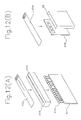
- Fig. 1 is a construction drawing of an input-output unit useful for the understanding of the present invention, in which (A) is a plan view, (B) is a front elevational view and (C) is a side elevational view.
- a card accommodating chamber 10 is provided with a plurality of slots 12 for accommodating input-output cards 50, and in this example there are 16 slots disposed in a row.
- An upper guide groove 12a and a lower guide groove 12b, oriented in the insertion direction of the input-output cards 50, are disposed as a pair in each slot 12.
- a back board 14 is mounted at the back of the card accommodating chamber 10, and connectors 16 are mounted on the back board 14 in correspondence with the slots 12.
- the connectors 16 connect with connectors 56 mounted on the back ends of the input-output cards 50; certain poles are connected to a terminal block part 20, and the other poles are connected to a bus connected to the system side.
- the terminal block part 20 has terminals in sets of two or three, and these sets of terminals correspond to the slots 12.
- the middle row terminals 22 are offset by half their pitch with respect to the lower row terminals 21 and the upper row terminals 23 in order facilitate the work of connecting the field device signal wires. It is desirable that terminals having mechanisms to prevent the screws falling out be used for these terminals, because this makes the installation work easier.
- a terminal cover 24 covers the lower row terminals 21, the middle row terminals 22 and the upper row terminals 23, and this terminal cover 24 can be opened and closed about a shaft part 27; when wire connecting work is to be carried out it is opened, and in the normal operating state it is closed, protecting the terminals.
- Universal receiving chambers 28 are mounted on the card accommodating chamber side of the terminal block part 20, and are used to mount RJC units for performing temperature compensation in cases when the signal wires are thermocouples and to connect backup apparatus when the control device is in a semiautomatic state, etc..
- a slot indicator sheet 25 and a terminal indicator sheet 26 are affixed to the front side and the back side respectively of the terminal cover 24; the details of these sheets will be described later.
- a connector connecting part 29 is provided for handling the same signals as the terminal block 20 or for handling other, different signals; it is also called a second output.
- the card accommodating chamber 10 and the terminal block 20 are mounted on the front of a case part 30, and system side connectors 40 are mounted on the back of this case 30.
- the case 30 is made of a material having good thermal conductivity such as aluminum or the like, and is also suitably provided with ventilation holes.
- the system side connectors 40 are connected to a back unit (not shown in the drawings), and for positioning purposes a pair of projecting portions 42 are provided on the back side of the case part 30.
- Mounting screws 44 are disposed at the four corners of the case part 30 and are used to mount the case part 30 on the back unit.
- the back unit is accommodated in a cabinet or the like, and is provided with a bus which is connected to the central control device of the system side.
- the input-output cards 50 input signals from the signal wires connected to the terminal block part 20, perform control computation on these signals, output control signals, and convert these inputted signals into signals for feeding into the bus which is connected to the connectors 16.
- the input-output cards 50 are assigned one-on-one to the signals that they handle, and in Fig. 1 one card only is installed in the card accommodating chamber 10 and the other slots are empty.
- Fig. 2 is a view illustrating the connection between the terminal block part 20 and the back board 14. It is necessary for each set of contacts of the terminal block part 20 to be connected to the poles of the connector 16, on the back board 14, of the corresponding slot 12.
- a terminal board 29' mounted on the back of the terminal block part 20 can be connected en bloc to the terminals of the back board 14, the wiring work can be done smoothly.
- the terminal board 29' and the back board 14 are constructed integrally using a printed circuit board of a rigidity such that it can be bent (a flex-rigid circuit board) 46, and the wiring patterns of both the terminal board 29' and the back board 14 should not be constructed of separate printed circuit boards, and the two connected by a multiple core flexible cable.
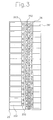
- Fig. 3 is a development view of the sheet which is affixed to the terminal cover 24.
- the slot indicator sheet 25 and the terminal indicator 26 are printed on either side of a fold line 263, and the sheet is folded into two along the fold line 263 and affixed to the terminal cover 24 in such a way as to cover the front and rear sides of the cover 24.
- the slot indicator sheet 25 is made up of a tag indicator column 251 and a slot number column 252, and the tag names of the input-output cards 50 inserted into the slots 12 are written in the tag indicator column 251.
- the terminal indicator sheet 26 is made up of a tag indicator column 261 and a terminal number column 262, and the tag names of the field devices connected are written in the tag indicator column 261.
- the lower row terminals 21, the middle row terminals 22 and the upper row terminals 23 of the terminal block part 20 are indicated in the terminal number column 262; the terminals of slot one are for example marked 1A, 1B, 1C.
- a 'tag name' is a name given to each object of control in order to distinguish the objects of control.
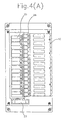
- Fig. 4 is a view illustrating the sheet affixed to the terminal cover 24, in which (A) shows the terminal cover closed and (B) shows the terminal cover open.
- the terminal cover 24 is closed, the slot indicator sheet 25 is seen. It is with the terminal closed like this that the input-output cards 50 are inserted into their respective slots 12, and the principle is that the tag name column 251 and the tag names on the input-output cards 50 should match.
- the terminal indicator sheet 26 When the terminal cover 24 is open, the terminal indicator sheet 26 is seen. In this position, the terminal indicator sheet 26 is alongside the sets of terminals of the terminal block part 20. Thus, during instrumenting work, the terminal number column 262 is close to the screw terminals, and confirmation of the terminal numbers is easy. Also, after a piece of wiring work has been completed, start-up is carried out, and, during such start-ups checking of the screw terminals and numbers can be carried out easily, and checking work can be done even when input-output cards 50 are not loaded into their slots 12.
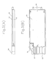
- FIG. 5 is a detailed construction drawing of the input-output card 50, in which (A) is a plan view, (B) is a side elevational view with the cover part 55 fitted, and (C) is a side elevational view with the cover part 55 removed.
- the printed circuit board 51 has electronic components which perform the signal conversion mounted on it, and is made to be of thin form by for example surface mounted components being mounted on both sides of it.
- a case part 52 gives the input-output card 50 its basic shape, and the printed circuit board 51 is mounted on this case part 52 and the case part 52 protects one side of the printed circuit board 51.
- a fan part 53 performs cooling, and preferably is made integrally with the case part 52 from die cast aluminum or the like, so that it can conduct heat smoothly.
- An ejector portion 54 is mounted on the end of the front of the case part 52, and is used when the card 50 is taken out of the card accommodation chamber 10.
- a cover 55 protects the other side of the printed circuit board 51, and is fitted to the case part 52.
- a connector 56 is mounted on the back of the input-output card 50, and mates with a connector 16.
- a light guide part 57 is mounted on the fan part 53, and guides light emitted by a light emitting device 58, which is mounted on the printed circuit board 51 and indicates the operating state of the input-output card 50, to the front of the input-output card 50.
- the ejector part 54 is mounted on the case part 52.
- the light guide part 57 is inserted into a fitting groove formed in the fan part 53.
- the printed circuit board 51 is then positioned in its predetermined position in the case 52 and fixed in place with screws. In this, by the printed circuit board being moved in the directions shown by the arrows b and c in Fig.5, positioning is carried out smoothly.
- the cover part 55 is fitted to the case part 52.
- a nameplate showing a tag is affixed to the front of the case part 52.
- the printed circuit board 51 is entirely covered by the case part 52 and the cover part 55, there is the benefit that there are no exposed electronic components and the reliability is good. For example, even if electrically conducting matter falls, there is no danger of shorting of the electronic components, and during handling also no outside forces act directly on the parts. And, although the input-output card 50 is accommodated in the card accommodation chamber 10, because the fan part 53 is exposed to the outside air, there is the benefit that heat generated on the printed circuit board 51 is conducted by the case part 52 and the cover part 55 to the fan part 53, is released into the outside air, and the heat dissipation efficiency is therefore good.
- Fig. 6 is a view illustrating the ejector part 54.
- the ejector part 54 has a lever portion 541 which provides an ejecting force, an engaging portion 542 having a recessed portion which engages with a window portion 16 formed in the card accommodation chamber 10, a shaft portion 543 which serves as a pivot, and a lock portion 544 which fixes the ejector part 54 to the case part 52.
- the lock portion 544 is a concave portion which engages with a convex portion 521 mounted on the side of the case part 52.
- Fig. 7 is a view illustrating the device which shows the operating state of the input-output card 50.
- the light emitting device 58 is mounted on the printed circuit board 51, and because light from the light emitting device 58 is guided to the front of the card by the light guide part 57, assemblability is good.
- a light emitting device of special shape has been used, but because in this preferred embodiment the light guide 57 is used, there is the benefit that the assemblability is good and relatively few components are required.
- FIG. 8 is a perspective construction drawing of a preferred embodiment of the present invention.
- An input-output nest 70 which can be made of aluminum when good heat dissipation is required, as in the case of the case part 30 discussed above, and can be made of plastic when heat dissipation need not be considered, has inside it two chambers which each accommodate two input-output printed circuit boards 80.
- the input-output printed circuit boards 80 have circuits which perform conversion between the signal forms used on the control device side and the signal forms used on the field devices side; because, for reasons relating to increasing the signal transfer speed, parallel signals are used in the bus, and, in order to keep down the number of cores, serial signals (in the case of digital signals) and analog signals are used in the signal wires, the input-output printed circuit boards 80 perform conversion of these signals.
- An interface section 90 has the field device side signal wires connected to it and sends and receives these signals to and from an input-output printed circuit board 80; it is of connector type for use with multiple core cable, and has indicators for indicating the state of the signals in the input-output printed circuit board 80.
- a terminal block 60 like the interface section 90, can have the field device side signal wires connected to it and is for sending and receiving these signals to and from an input-output printed circuit board 80; it is used in cases when the signal wires are separate, individual wires.
- Fig. 9 is a construction view of a connector-type interface section 90 fitted to an input-output nest.
- a back unit 100 is a plate member which is accommodated in a cabinet or a console, and is provided with a bus which is connected to the central control device.
- the printed circuit boards 80 which are fitted to the back unit 100 are each provided with a front connector 81 for connections to the interface section 90 or a terminal block 60 and a rear connector 82 for connections to the input-output nest 70.
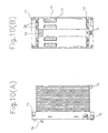
- Fig. 10 is a detailed construction view of the input-output nest 70, in which (A) is a side elevational view and (B) is a front elevational view.
- a back board 71 is mounted at the back of the input-output nest 70, and connectors 72 used for connections to the printed circuit board 80 are mounted on the back board 71.
- Card guide portions 73 guide the printed circuit boards 80 in the insertion direction and ensure the connection of the connectors 72 with the rear connectors 82; the card guide portions are also called slots.
- a wiring work area 74 is provided in the central portion of the front of the input-output nest 70, and, because the chambers which accommodate the printed circuit boards 80 are located on each side of this, the wiring work area 74 is also a wall separating these two chambers.
- An earth part 75 is a group of terminals mounted at the bottom of the wiring work area 74, and terminals for earthling the printed circuit boards 80 with respect to the box body are mounted here.
- An metal earthling fitting 76 provides earthling when the input-output nest is fitted to the back unit 100.
- Mounting screws 77 are used to mount the input-output unit 70 on the back unit 100; in this example, a mounting screw 77 is provided at each of the four corners of the input-output nest 70.
- Interface fitting portions 78 are provided near the card guide portions 73, and are fitting holes for fitting the interfaces 90 to the slots.
- Projecting portions 79 are rod-shaped projections mounted on the back face of the input-output nest 70, and engage with concave portions provided in the back unit 100 and facilitate positioning.
- the projecting portions 79 are provided in two places, a connector (not shown in the drawings) is disposed between them, and they guide the mating of this connector with a connector on the back unit side.
- a connector (not shown in the drawings) is disposed between them, and they guide the mating of this connector with a connector on the back unit side.
- the amount of heat produced by the input-output printed circuit board 80 varies, depending on the type of signals handled and the signal conversion method.
- the input-output nest 70 is provided with slit-form openings for heat dissipation, and is designed so that for up to a certain amount of generated heat the increase in the interior temperature remains at tolerable value. According to the amount of heat generated by the input-output printed circuit board 80 and the quantity of components mounted on it, although each chamber is capable of accommodating two boards, one circuit board may be accommodated in each chamber, or altogether one board only may be accommodated in the two chambers.
- the connecting work can be carried out smoothly.
- the width of the interface section 90 can be one slot width or two slot widths, or in some cases may be made wider, occupying the wiring work area 74. Because this kind of wide interface section 90 is allowed, there is a high degree of design freedom.
- an industrial control equipment input-output unit is constructed from the three modules that are the general input-output nest 70, the input-output printed circuit board 80 which performs signal conversion, and the interface 90 or the terminal block 60, and these are combined according to the requirements of the system to be served, there are the benefits that the system can be built with a standardized nest form, expansion and alterations can be done easily, and cost reductions based on mass-production can be sought.
- Fig. 11 is a schematic construction view of the terminal block 60, in which (A) is an upper surface view and (B) is a side elevational view.
- the terminal block 60 is made of an insulating material such as plastic, and is provided with a lower terminal row 611 and an upper terminal row 612, each row having 17 terminals.
- a ready indicator chamber 616 and a circuit board accommodating chamber 618 divided into four chambers are disposed in a row parallel to the lower terminal row 611 and the upper terminal row 612, and the chambers of the circuit board chamber 618 are separated from each other by circuit board guides 619.
- a back board 62 is mounted on the bottom of the terminal block 60, and has a wiring pattern which is connected to the terminals.
- a connector 63 is mounted on the bottom of the back board 62, and sends the signals from the signal wires connected to the terminals out through a connector (not shown in the drawings) connected to an outside device.
- An indicator circuit board 64 is accommodated in the circuit board accommodation chamber 618, and in this example light emitting devices 642 are shown mounted on the indicator circuit board 64, but when other expansion functions such as temperature compensation units are to be provided, other option circuit boards are fitted.
- Fig. 12 is a view illustrating an expansion function to be fitted into the circuit board accommodation chamber, in which (A) shows the case of a indicator function and (B) shows the case of a temperature compensation unit.
- a indicator circuit board 64 is used in the case of the indicator function.
- the indicator circuit board 64 has light emitting devices 642 mounted on it in four groups corresponding to the circuit board accommodating chamber 618 which is divided into four chambers, and spaces corresponding to the circuit board guides 619 are provided between the groups of light emitting devices.
- the circuit board guides 619 also perform the function of confining the indicator circuit board 64 to its prescribed position.
- An partitioned light guide part 644 is a member formed of an opaque plastic; the partitioned light guide part 644 is mounted on the upper surfaces of the circuit board guides 619, and accommodates the light emitting devices 642 in light guide holes 645.
- An indicator sheet 652 is affixed to the upper surface of the partitioned light guide part 644 and indicates the terminal numbers corresponding to the light emitting devices 642 which light up and go out in the light guide holes 645.
- the temperature compensation unit 66 makes contact with the terminals and measures their temperature, and is necessary when an accurate temperatures are to be measured with thermocouples.
- one unit is provided for four terminals.
- a cover sheet 668 is fitted onto the surface of the terminal side of the temperature compensation unit 66; windows are formed in the side which faces the terminals, and temperature sensors are pushed against the terminals.
- a ready sheet 654 is affixed to the upper surface of the temperature compensation unit 66; the ready sheet 654 serves the indicator in the ready indicator chamber 616, and there is no particular indication on the circuit board accommodation chambers 618 portion.
- Fig. 13 is a cross-sectional view of a terminal block which has a indicator function.
- the terminal constructions in the chambers of the lower terminal row 611 and the upper terminal row 612 are omitted in this view, but for example the terminals having screw falling prevention mechanisms disclosed in Japanese Laid-Open Utility Model Publication No. H4-102568 are suitable.
- a main body 61 is the main structural member of the terminal block 60, and is made of plastic.
- a back plate 614 covers a back board 62, and is fitted to the bottom surface of the terminal block 60.
- a connecting cable 622 connects the back board 62 to the indicator circuit board 64, and supplies signals for controlling the illumination of the light emitting devices 642 from the back board 62 side.
- the light emitting devices are bent in the end surface direction of the indicator circuit board 64 and are received by the partitioned light guide part 644.
- a cover 65 opens and closes about a hinge part 651 mounted on the terminal block 60; when the cover is opened, signal line connection work on the terminals can be performed easily, and when the cover 65 is closed, the indicator sheet 652 is positioned above the partitioned light guide part 644 and the operator can easily discern which of the terminals it is whose state is being indicated by the light emitting devices 642.
- Fig. 14 is a cross-sectional view of a terminal block having a temperature compensation unit 66.
- the temperature compensation unit 66 has a case portion 661 of an external shape suitable for insertion into the circuit board accommodation chamber 618, and a printed circuit board 662 is accommodated inside it.
- a spring 663 is mounted between the case portion 661 and the printed circuit board 662, and by pushing the printed circuit board 662 to the terminal side this spring 663 causes the temperature sensors 664 to make contact with the terminals.
- a metal holding fitting 665 has its entirety fixed to the printed circuit board 662, and the temperature sensors 664 are mounted integrally with it.
- a cable 666 carries the measurement signal produced by the temperature sensor 664 to the back board 62 through a compensation connector 667 after it has been converted into an electronic signal by the printed circuit board 662.
- the connection work of the signal wires is carried out smoothly. It is noted that because thermocouple temperature compensation is basic instrumentation engineering knowledge, an explanation of it here is omitted.
- Fig. 15 is a cross-sectional view illustrating the details of the ready indicator chamber 616.
- a light emitting device 626 is mounted at the edge of the back board 62, and the operating state of the terminal block 60 is indicated by this light emitting device 626.
- a light guide 624 is accommodated in the ready indicator chamber 616, and this light guide 624 guides the light emitted by the light emitting device 626 to the RDY of the indicator sheet 652. This function is an essential function of the terminal block, and is provided commonly for all types of terminal block.
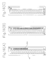
- Fig. 16 is a plan view of the terminal block main body with the indicator sheet affixed to it, in which (A) shows a sixteen contact point indicator, (B) shows a thirty-two point indicator and (C) shows a indicator for the ready signal only.
- the indicator function is sixteen points
- corresponding terminals of the lower terminal row 611 and the upper terminal row 612 are used as sets of one plus terminal and one minus terminal. Accordingly, the contact point signal indication is also performed using the signals of the terminal sets.
- the ready signal RDY and the contact point terminal numbers 1 ⁇ 16 are indicated on the indicator sheet 652, and this makes easy the visual confirmation of which of the terminals corresponds to which of the light emitting devices 642 accommodated in the circuit board accommodation chamber 618.
- Ready sheet 654 is fixed on the terminal block 60 and it shows only the ready signal RDY in cases such as when the temperature compensation unit 66 is accommodated in the circuit board accommodation chamber 618, and when the indicator circuit board 64 is not fitted. Because the ready signal RDY is necessary for all the types of terminal, by this the operating state of the terminal block can be confirmed.
- the operating state of the terminal block is indicated by the ready indicator 616
- the operating state of the terminal block can be checked whatever the type of the terminals, and there is the benefit that the common use of the terminal block 60 can be promoted and few molds are required.
- the indicator circuit board 64 and the temperature compensation unit 66 and the like are provided or not provided case-by-case, according to the requirements of each type of terminal block, there is the benefit that optional functions matched to the signal line type can be realized with a small number of components.
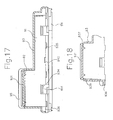
- Fig. 17 is a construction drawing showing a preferred embodiment of the connector-type interface section 90, with the case being shown with hatching lines.
- a printed circuit board 91 has electronic devices and connecters, etc., mounted on it, and is roughly L-shaped.
- a indicator circuit board 92 is provided with light emitting devices such as LEDs disposed in a matrix form, and makes a T-shape in its positional relationship with the printed circuit board 91.
- the printed circuit board 91 is accommodated in the case 93 side surface direction, and the indicator circuit board 92 is accommodated behind an indicator window 931 mounted at the front of the case 93.
- a cover 94 is fitted to the back of the case 93, and holds both the printed circuit board 91 and the indicator circuit board 92 in the case 93.
- a box body for electronic apparatus such as the input-output nest shown in Fig. 8, is fitted to this case 93, and an input-output printed circuit board 80 for signal processing is also connected to the case 93 via a connector 911.
- an indicator window cover 95 made of transparent plastic or the like be fitted over the indicator window 931.
- Fig. 18 is an enlarged view of the vicinity of the indicator window 931.
- Holding projections 937, which position the indicator circuit board 92, and indicator circuit board abutting portions 939, which abut with the indicator window 931 side edge of the indicator circuit board 92, are provided on the back of the indicator window 931.
- the indicator circuit board abutting portions 939 are line-form projections mounted in the widthways direction of the indicator window 931.
- Fig. 19 is a development parts view, with the cover 94 removed.
- Windows corresponding to the light emitting devices are formed in a four row by eight column matrix layout in the indicator window 931.
- a indicator circuit board accommodation chamber 932 is located behind the indicator window 931 and accommodates the indicator circuit board 92.
- a printed circuit board accommodating chamber 933 occupies most of the case 93 and accommodates the printed circuit board 91.
- Engaging holes 934 are engaged with by case mounting claws 941 mounted on the cover 94, and in this example consist of rectangular windows formed in two places on each side of the case 93.
- Cover guide projecting portions 935 are for facilitating the mating of the case 93 and the cover 94, and thin portions which are thinner than the rest of the cover 94 are formed in corresponding positions on the cover 94 side. Case guide projections can be provided on the cover 94 side also, and thin portions can be formed on the case 93 side.
- Nest mounting portions 936 are screw holes formed in the upper and lower ends of the surface of the case 93 which abuts with the cover 94, and are used in fitting the case 93 to a nest or a wall body or the like.
- a connector 911 is mounted on the back of the printed circuit board 91, and this is connected to an input-output printed circuit board 80 for signal processing.
- a connector 912 is mounted on the front of the printed circuit board 91, and this is used in connecting signal wires connected to outside devices. Signals inputted through the connector 912 pass through the connector 912 and the input-output printed circuit board 80 and are used in connection with the bus that is on the nest side.
- the cable 922 is a multiple core flat cable which connects the printed circuit board 91 and the indicator circuit board 92 and carries the illumination drive signals of the indicator circuit board 92.
- Holding holes 921 are openings which are provided in two locations on the indicator circuit board 92 and engage with the holding projections 937. To allow for dimensional errors these holes are oblong in shape.
- Fig. 20 is a component view of the case 93, in which (A) is a front elevational view, (B) is a side elevational view, and (C) is a back elevational view.
- a connector fitting hole 96 has a cable which connects with the connector 912 fitted to the printed circuit board 91 fitted to it, and, in order to perform the connection completely, screw holes are formed at both ends.
- Circuit board holding grooves 938 are portions cut out of ribs formed in the widthways direction of the case 93, and position the printed circuit board 91.
- the holding projections 937 are disposed in positions where they do not overlap with the circuit board holding grooves 938.
- the cover 94 is also provided with a connector mounting hole 96 for fitting the cable connecting with the connector 911 mounted on the printed circuit board 91.
- the indicator circuit board 92 is fitted onto the back of the indicator window 931 in such a way that the holding projections 937 on the indicator window 931 engage with the holding holes 921. Then, the printed circuit board 91 is inserted along the circuit board holding grooves 938 and thereby accommodated in the circuit board accommodation chamber 933. During this process, differences in attitude between the indicator circuit board 92 and the printed circuit board 91 are absorbed by the cable 922. Finally, when the cover 94 is fitted to the case 93, the indicator circuit board 92 and the printed circuit board 91 are fixed in the case together, en bloc.
Description
Claims (5)
- An input-output unit for performing signal receiving and delivery mediation between an industrial control equipment and field devices controlled by it, the input-output unit comprisingan input-output nest (70), suitable to be connected by a bus to the industrial control equipment,an input-output printed circuit board (80), which is accommodated in the input-output nest (70) and performs conversion between the signal forms handled by the industrial control equipment and the signal forms handled by the field devices;a front connector (81) provided at the edge of the input-output printed circuit board(80) so as to be set at the front of the input-output nest (70);a terminal block (60) comprising arranged terminals, which are lined up in a plurality of rows and suitable to be connected to the field device side signal wires, in cases when the signal wires are separate, individual wires, and suitable to be connected to the front connector (81);an interface section (90) suitable to be connected to the field device side signal wires in cases when the signal wires have a connector for use with multiple core cable, and suitable to be connected to the front connector (81);wherein either the terminal block (60) or the interface section (90) is selectively fitted to the front connector (81) and the input-output nest (70).
- An input-output unit according to claim 1, wherein the terminal block (60) has a ready indicator chamber (616) and a circuit board accommodation chamber (618), both chambers being disposed in the row direction in which the terminals are disposed, and has a back board (62) mounted on the bottom surface of the terminal block (60), which has a pattern which is connected to the terminals, and wherein in the ready indicator chamber (616) light emitted by a light emitting device (626), mounted on the back board (62), for indicating the operating state of the terminal block (60), is guided to the upper surface of the terminal block (60).
- An input-output unit according to claim 2, wherein an indicator circuit board (64) on which light emitting devices (642), which light up and go out according to the signal states of the terminals, is accommodated in the circuit board accommodation chamber (618), and wherein an partitioned light guide part (644) which is on the upper surface of the terminal block (60) and which in the direction in which the terminals are lined up separately displays the light emitted by each of these light emitting devices, is mounted in the circuit board accommodation chamber (618).
- An input-output unit according to claim 2, wherein a temperature compensation unit (66), which makes thermal contact with a terminal to which a thermocouple is connected and measures the temperature of that terminal, is mounted in the circuit board accommodation chamber (618).
- An input-output unit according to claim 1, wherein the interface section (90) comprises a printed circuit board (91) and an indicator circuit board (92) which has light emitting devices mounted on it and is connected to this printed circuit board (91) through a cable (922), a case (93) whose side surface is larger than the printed circuit board (91) and which accommodates the indicator circuit board (92) behind an indicator window (931) provided in the front of the case (93), and a cover (94) which is fitted to the back of the case (93), and wherein the indicator circuit board (92)is provided with holding holes (921) and the indicator window (931) is provided with holding projections (937) which project from the back surface of the display window and engage with the holding holes (921) and the indicator circuit board (92) is held by the holding projections (937) and an edge portion of the printed circuit board (91).
Applications Claiming Priority (10)
| Application Number | Priority Date | Filing Date | Title |
|---|---|---|---|
| JP29236/93 | 1993-02-18 | ||
| JP2923693 | 1993-02-18 | ||
| JP05029236A JP3139693B2 (en) | 1993-02-18 | 1993-02-18 | I / O unit |
| JP31824/93 | 1993-02-22 | ||
| JP5031824A JP2845076B2 (en) | 1993-02-22 | 1993-02-22 | I / O unit |
| JP3182493 | 1993-02-22 | ||
| JP3802193 | 1993-02-26 | ||
| JP38021/93 | 1993-02-26 | ||
| JP5038021A JP2910479B2 (en) | 1993-02-26 | 1993-02-26 | Terminal block |
| EP94100450A EP0612205B1 (en) | 1993-02-18 | 1994-01-13 | Input-output unit |
Related Parent Applications (1)
| Application Number | Title | Priority Date | Filing Date |
|---|---|---|---|
| EP94100450.9 Division | 1994-01-13 |
Publications (3)
| Publication Number | Publication Date |
|---|---|
| EP0713360A2 EP0713360A2 (en) | 1996-05-22 |
| EP0713360A3 EP0713360A3 (en) | 1996-08-14 |
| EP0713360B1 true EP0713360B1 (en) | 2000-03-29 |
Family
ID=27286475
Family Applications (2)
| Application Number | Title | Priority Date | Filing Date |
|---|---|---|---|
| EP96102172A Expired - Lifetime EP0713360B1 (en) | 1993-02-18 | 1994-01-13 | Input-output unit |
| EP94100450A Expired - Lifetime EP0612205B1 (en) | 1993-02-18 | 1994-01-13 | Input-output unit |
Family Applications After (1)
| Application Number | Title | Priority Date | Filing Date |
|---|---|---|---|
| EP94100450A Expired - Lifetime EP0612205B1 (en) | 1993-02-18 | 1994-01-13 | Input-output unit |
Country Status (4)
| Country | Link |
|---|---|
| US (1) | US5483229A (en) |
| EP (2) | EP0713360B1 (en) |
| DE (3) | DE69406327T2 (en) |
| SG (1) | SG43191A1 (en) |
Families Citing this family (44)
| Publication number | Priority date | Publication date | Assignee | Title |
|---|---|---|---|---|
| EP0700241A1 (en) * | 1994-09-01 | 1996-03-06 | Siemens Aktiengesellschaft | Device to indicate operating states of slidable electronic units |
| FR2730350A1 (en) * | 1995-02-07 | 1996-08-09 | Schneider Electric Sa | COMPOSABLE ELECTRICAL INTERFACING DEVICE |
| USD384037S (en) * | 1995-04-07 | 1997-09-23 | Kabushiki Kaisha Toshiba | Process monitoring controller |
| US5947748A (en) * | 1996-09-30 | 1999-09-07 | Siemens Energy & Automation, Inc. | Connector for programmable logic controller having modifiable termination therefor |
| JP3090071B2 (en) * | 1996-11-29 | 2000-09-18 | オムロン株式会社 | Control device |
| US6417774B1 (en) | 1997-10-30 | 2002-07-09 | Fireeye Development Inc. | System and method for identifying unsafe temperature conditions |
| US6563533B1 (en) * | 1998-01-06 | 2003-05-13 | Sony Corporation | Ergonomically designed apparatus for selectively actuating remote robotics cameras |
| US6850415B2 (en) * | 1998-12-31 | 2005-02-01 | Honeywell International Inc. | Methods and apparatus for circuit integration |
| DE20009207U1 (en) | 2000-05-22 | 2001-09-27 | Ceag Sicherheitstechnik Gmbh | Device for signal transmission |
| US6995665B2 (en) * | 2002-05-17 | 2006-02-07 | Fireeye Development Incorporated | System and method for identifying, monitoring and evaluating equipment, environmental and physiological conditions |
| US20050001728A1 (en) * | 2003-06-27 | 2005-01-06 | Appelt Daren R. | Equipment and method for identifying, monitoring and evaluating equipment, environmental and physiological conditions |
| US8085144B2 (en) | 2002-07-02 | 2011-12-27 | Mine Safety Appliances Company | Equipment and method for identifying, monitoring and evaluating equipment, environmental and physiological conditions |
| JP3788420B2 (en) * | 2002-11-26 | 2006-06-21 | 日本電気株式会社 | rack |
| US8540493B2 (en) | 2003-12-08 | 2013-09-24 | Sta-Rite Industries, Llc | Pump control system and method |
| US7073971B2 (en) * | 2004-02-10 | 2006-07-11 | Egs Electrical Group, Llc | Apparatus and methods for detachably mounting devices to rails |
| US8019479B2 (en) | 2004-08-26 | 2011-09-13 | Pentair Water Pool And Spa, Inc. | Control algorithm of variable speed pumping system |
| US8043070B2 (en) | 2004-08-26 | 2011-10-25 | Pentair Water Pool And Spa, Inc. | Speed control |
| US7874808B2 (en) | 2004-08-26 | 2011-01-25 | Pentair Water Pool And Spa, Inc. | Variable speed pumping system and method |
| US7845913B2 (en) | 2004-08-26 | 2010-12-07 | Pentair Water Pool And Spa, Inc. | Flow control |
| US8602745B2 (en) | 2004-08-26 | 2013-12-10 | Pentair Water Pool And Spa, Inc. | Anti-entrapment and anti-dead head function |
| US8469675B2 (en) | 2004-08-26 | 2013-06-25 | Pentair Water Pool And Spa, Inc. | Priming protection |
| US7686589B2 (en) | 2004-08-26 | 2010-03-30 | Pentair Water Pool And Spa, Inc. | Pumping system with power optimization |
| US8480373B2 (en) | 2004-08-26 | 2013-07-09 | Pentair Water Pool And Spa, Inc. | Filter loading |
| US7130196B2 (en) * | 2005-01-19 | 2006-10-31 | General Electric Company | Apparatus and method for transferring heat from control devices |
| US7670148B2 (en) * | 2006-01-21 | 2010-03-02 | Shaltech, Inc. | Automation controller I/O module |
| AU2009302593B2 (en) | 2008-10-06 | 2015-05-28 | Danfoss Low Power Drives | Method of operating a safety vacuum release system |
| DE102008058090B4 (en) * | 2008-11-18 | 2021-08-26 | Abb Ag | Input / output module for an automation device |
| US8564233B2 (en) * | 2009-06-09 | 2013-10-22 | Sta-Rite Industries, Llc | Safety system and method for pump and motor |
| US9556874B2 (en) | 2009-06-09 | 2017-01-31 | Pentair Flow Technologies, Llc | Method of controlling a pump and motor |
| US8436559B2 (en) * | 2009-06-09 | 2013-05-07 | Sta-Rite Industries, Llc | System and method for motor drive control pad and drive terminals |
| US8579639B2 (en) | 2010-08-20 | 2013-11-12 | Rockwell Automation Technologies, Inc. | Systems and methods for coupling input/output devices |
| US9055687B2 (en) * | 2010-08-20 | 2015-06-09 | Rockwell Automation Technologies, Inc. | Input/output circuits and devices having physically corresponding status indicators |
| WO2012077205A1 (en) * | 2010-12-08 | 2012-06-14 | 三菱電機株式会社 | Electronics unit |
| BR112013014476A2 (en) | 2010-12-08 | 2016-09-20 | Pentair Water Pool & Spa Inc | vacuum relief relief valve for a vacuum release safety system |
| US9885360B2 (en) | 2012-10-25 | 2018-02-06 | Pentair Flow Technologies, Llc | Battery backup sump pump systems and methods |
| USD772172S1 (en) * | 2014-01-29 | 2016-11-22 | Yokogawa Electric Corporation | Signal I/O module |
| US9762107B2 (en) | 2014-04-01 | 2017-09-12 | Rockwell Automation Technologies, Inc. | Radiation heat transfer of internal motor components by electro-magnetic waves |
| USD774004S1 (en) * | 2015-03-27 | 2016-12-13 | Honeywell International Inc. | RTU IO module with expansion end plate |
| USD772173S1 (en) * | 2015-06-26 | 2016-11-22 | Yokogawa Electric Corporation | I/O module unit |
| TWI582704B (en) * | 2016-08-05 | 2017-05-11 | Primax Electronics Ltd | Mrthod for fabricating fingerprint identifying module |
| US9861002B1 (en) * | 2016-10-20 | 2018-01-02 | Rockwell Automation Technologies, Inc. | Single channel I/O in a modular sub-chassis |
| US10251303B2 (en) * | 2017-05-05 | 2019-04-02 | Dell Products, Lp | Server display for displaying server component information |
| US20190348778A1 (en) * | 2018-02-17 | 2019-11-14 | Rodney Preston | Printed Circuit Board for Interconnecting Electrical Control Wires |
| US10838386B1 (en) | 2019-09-26 | 2020-11-17 | Rockwell Automation Technologies, Inc. | Distributed modular I/O device with configurable single-channel I/O submodules |
Family Cites Families (11)
| Publication number | Priority date | Publication date | Assignee | Title |
|---|---|---|---|---|
| US3992654A (en) * | 1975-03-26 | 1976-11-16 | Allen-Bradley Company | Disconnect arm for electrical equipment |
| DE2928668A1 (en) * | 1979-07-16 | 1981-02-12 | Siemens Ag | Insertable light conductor strip - has optic fibres aligned with LEDs in display of printed circuit board edge connector |
| US4401351A (en) * | 1981-09-28 | 1983-08-30 | Advant Corporation | Expandable card cage |
| US4511950A (en) * | 1983-06-27 | 1985-04-16 | Northern Telecom Limited | Backpanel assemblies |
| DE3502295A1 (en) * | 1985-01-24 | 1986-07-24 | ANT Nachrichtentechnik GmbH, 7150 Backnang | CONSTRUCTION SYSTEM FOR ELECTRICAL COMMUNICATION DEVICES |
| US4872212A (en) * | 1987-05-15 | 1989-10-03 | Eip Microwave, Inc. | Microwave main frame |
| US5253140A (en) * | 1988-03-12 | 1993-10-12 | Fanuc Ltd. | Connector unit for input/output module of programmable controller having disengagement lever |
| US4920453A (en) * | 1988-10-13 | 1990-04-24 | Allen-Bradley Company, Inc. | Programmable controller module |
| US5103378A (en) * | 1990-09-21 | 1992-04-07 | Virginia Panel Corporation | Hinged interlocking receiver for mainframe card cage |
| DE9102101U1 (en) * | 1991-02-22 | 1992-06-25 | Kloeckner-Moeller Gmbh, 5300 Bonn, De | |
| US5436794A (en) * | 1994-08-31 | 1995-07-25 | Allen-Bradley Company, Inc. | Industrial controller card rack with heat transfer across card edges |
-
1994
- 1994-01-03 US US08/176,923 patent/US5483229A/en not_active Expired - Lifetime
- 1994-01-13 DE DE69406327T patent/DE69406327T2/en not_active Expired - Lifetime
- 1994-01-13 SG SG1996005235A patent/SG43191A1/en unknown
- 1994-01-13 DE DE0612205T patent/DE612205T1/en active Pending
- 1994-01-13 EP EP96102172A patent/EP0713360B1/en not_active Expired - Lifetime
- 1994-01-13 DE DE69423764T patent/DE69423764T2/en not_active Expired - Lifetime
- 1994-01-13 EP EP94100450A patent/EP0612205B1/en not_active Expired - Lifetime
Also Published As
| Publication number | Publication date |
|---|---|
| DE612205T1 (en) | 1995-06-14 |
| DE69406327D1 (en) | 1997-11-27 |
| EP0713360A2 (en) | 1996-05-22 |
| EP0612205B1 (en) | 1997-10-22 |
| US5483229A (en) | 1996-01-09 |
| SG43191A1 (en) | 1997-10-17 |
| DE69423764D1 (en) | 2000-05-04 |
| EP0713360A3 (en) | 1996-08-14 |
| DE69423764T2 (en) | 2000-10-05 |
| DE69406327T2 (en) | 1998-04-16 |
| EP0612205A1 (en) | 1994-08-24 |
Similar Documents
| Publication | Publication Date | Title |
|---|---|---|
| EP0713360B1 (en) | Input-output unit | |
| US5099391A (en) | Housing for a rack mountable power supply for use with a programmable logic controller | |
| US4985845A (en) | Modular electrical control distribution system | |
| US9089067B2 (en) | Modular automation system | |
| US5472347A (en) | System for interconnecting I/O modules for data communications over a common backplane | |
| EP0242970B1 (en) | Fault tolerant modular computing system | |
| US7666004B2 (en) | Devices, systems, and/or methods regarding a programmable logic controller | |
| US4039902A (en) | Electronic automation system | |
| JP2515710B2 (en) | Front plug-in device | |
| US4215386A (en) | Modular panel construction for programmable controller | |
| US4217624A (en) | Communications interface adapter | |
| US5612680A (en) | Universal termination module for assembling wire harnesses having multiple diverse connectors | |
| US5214621A (en) | Universal circuit board housing with a hinged member | |
| US20070279892A1 (en) | Electrical power connection with two power connnectors on a module in an electronic system | |
| US20050074222A1 (en) | Plug-in unit, a housing and an electronic apparatus | |
| DE102004056363B4 (en) | Flexible expandable automation device | |
| US4333696A (en) | Plural edge P.C. board interconnection | |
| CN101512839A (en) | Electric addition module for assembling device, combination of addition module and assembling device as well as addition module set | |
| US5731951A (en) | Disk drive add-on device having disk drive with air passages and support with air passages | |
| EP1848258B1 (en) | Computer device with a modular transmission interface, the modular transmission interface, and an adaptor board | |
| WO2017074351A1 (en) | Fan connector housing | |
| ZA822123B (en) | A magazine for plug-in electrical assemblies | |
| EP4354666A1 (en) | System for connecting two controller system modules | |
| US20090221166A1 (en) | Electrical device with an i/o wiring interface | |
| WO2019151711A1 (en) | Adapter for changing connector pitch and method for manufacturing same |
Legal Events
| Date | Code | Title | Description |
|---|---|---|---|
| PUAI | Public reference made under article 153(3) epc to a published international application that has entered the european phase |
Free format text: ORIGINAL CODE: 0009012 |
|
| 17P | Request for examination filed |
Effective date: 19960214 |
|
| AC | Divisional application: reference to earlier application |
Ref document number: 612205 Country of ref document: EP |
|
| AK | Designated contracting states |
Kind code of ref document: A2 Designated state(s): DE GB NL |
|
| PUAL | Search report despatched |
Free format text: ORIGINAL CODE: 0009013 |
|
| AK | Designated contracting states |
Kind code of ref document: A3 Designated state(s): DE GB NL |
|
| GRAG | Despatch of communication of intention to grant |
Free format text: ORIGINAL CODE: EPIDOS AGRA |
|
| 17Q | First examination report despatched |
Effective date: 19990324 |
|
| GRAG | Despatch of communication of intention to grant |
Free format text: ORIGINAL CODE: EPIDOS AGRA |
|
| GRAH | Despatch of communication of intention to grant a patent |
Free format text: ORIGINAL CODE: EPIDOS IGRA |
|
| GRAH | Despatch of communication of intention to grant a patent |
Free format text: ORIGINAL CODE: EPIDOS IGRA |
|
| GRAA | (expected) grant |
Free format text: ORIGINAL CODE: 0009210 |
|
| AC | Divisional application: reference to earlier application |
Ref document number: 612205 Country of ref document: EP |
|
| AK | Designated contracting states |
Kind code of ref document: B1 Designated state(s): DE GB NL |
|
| REF | Corresponds to: |
Ref document number: 69423764 Country of ref document: DE Date of ref document: 20000504 |
|
| EN | Fr: translation not filed | ||
| PLBE | No opposition filed within time limit |
Free format text: ORIGINAL CODE: 0009261 |
|
| STAA | Information on the status of an ep patent application or granted ep patent |
Free format text: STATUS: NO OPPOSITION FILED WITHIN TIME LIMIT |
|
| 26N | No opposition filed | ||
| REG | Reference to a national code |
Ref country code: GB Ref legal event code: IF02 |
|
| PGFP | Annual fee paid to national office [announced via postgrant information from national office to epo] |
Ref country code: GB Payment date: 20130109 Year of fee payment: 20 Ref country code: DE Payment date: 20130109 Year of fee payment: 20 |
|
| PGFP | Annual fee paid to national office [announced via postgrant information from national office to epo] |
Ref country code: NL Payment date: 20130116 Year of fee payment: 20 |
|
| REG | Reference to a national code |
Ref country code: DE Ref legal event code: R071 Ref document number: 69423764 Country of ref document: DE |
|
| REG | Reference to a national code |
Ref country code: DE Ref legal event code: R071 Ref document number: 69423764 Country of ref document: DE |
|
| REG | Reference to a national code |
Ref country code: NL Ref legal event code: V4 Effective date: 20140113 |
|
| REG | Reference to a national code |
Ref country code: GB Ref legal event code: PE20 Expiry date: 20140112 |
|
| PG25 | Lapsed in a contracting state [announced via postgrant information from national office to epo] |
Ref country code: DE Free format text: LAPSE BECAUSE OF EXPIRATION OF PROTECTION Effective date: 20140114 Ref country code: GB Free format text: LAPSE BECAUSE OF EXPIRATION OF PROTECTION Effective date: 20140112 |