EP0706887B1 - Inkjet array and method of producing the same - Google Patents
Inkjet array and method of producing the same Download PDFInfo
- Publication number
- EP0706887B1 EP0706887B1 EP95202558A EP95202558A EP0706887B1 EP 0706887 B1 EP0706887 B1 EP 0706887B1 EP 95202558 A EP95202558 A EP 95202558A EP 95202558 A EP95202558 A EP 95202558A EP 0706887 B1 EP0706887 B1 EP 0706887B1
- Authority
- EP
- European Patent Office
- Prior art keywords
- piezoelectric
- plate
- piezoelectric elements
- inkjet array
- ink
- Prior art date
- Legal status (The legal status is an assumption and is not a legal conclusion. Google has not performed a legal analysis and makes no representation as to the accuracy of the status listed.)
- Expired - Lifetime
Links
- 239000004033 plastic Substances 0.000 claims description 15
- 229920003023 plastic Polymers 0.000 claims description 15
- 239000007788 liquid Substances 0.000 claims description 4
- 238000010438 heat treatment Methods 0.000 claims description 3
- 239000007787 solid Substances 0.000 claims description 3
- 229910010293 ceramic material Inorganic materials 0.000 claims description 2
- 239000000976 ink Substances 0.000 description 43
- 239000000463 material Substances 0.000 description 7
- 238000010276 construction Methods 0.000 description 5
- 239000000919 ceramic Substances 0.000 description 3
- 239000012943 hotmelt Substances 0.000 description 3
- 239000002184 metal Substances 0.000 description 3
- 238000003491 array Methods 0.000 description 2
- 230000015572 biosynthetic process Effects 0.000 description 2
- 238000005266 casting Methods 0.000 description 2
- 238000004519 manufacturing process Methods 0.000 description 2
- 239000004809 Teflon Substances 0.000 description 1
- 229920006362 Teflon® Polymers 0.000 description 1
- 238000004026 adhesive bonding Methods 0.000 description 1
- 239000003054 catalyst Substances 0.000 description 1
- 238000004891 communication Methods 0.000 description 1
- 239000004020 conductor Substances 0.000 description 1
- 239000003431 cross linking reagent Substances 0.000 description 1
- 230000003247 decreasing effect Effects 0.000 description 1
- 238000006073 displacement reaction Methods 0.000 description 1
- 230000000694 effects Effects 0.000 description 1
- 229920001971 elastomer Polymers 0.000 description 1
- 230000002349 favourable effect Effects 0.000 description 1
- 238000006459 hydrosilylation reaction Methods 0.000 description 1
- 230000010354 integration Effects 0.000 description 1
- 230000007257 malfunction Effects 0.000 description 1
- 238000002844 melting Methods 0.000 description 1
- 230000008018 melting Effects 0.000 description 1
- 238000012856 packing Methods 0.000 description 1
- 239000005060 rubber Substances 0.000 description 1
- 229920002379 silicone rubber Polymers 0.000 description 1
- 239000000126 substance Substances 0.000 description 1
- 230000001960 triggered effect Effects 0.000 description 1
Images

Classifications
-
- B—PERFORMING OPERATIONS; TRANSPORTING
- B41—PRINTING; LINING MACHINES; TYPEWRITERS; STAMPS
- B41J—TYPEWRITERS; SELECTIVE PRINTING MECHANISMS, i.e. MECHANISMS PRINTING OTHERWISE THAN FROM A FORME; CORRECTION OF TYPOGRAPHICAL ERRORS
- B41J2/00—Typewriters or selective printing mechanisms characterised by the printing or marking process for which they are designed
- B41J2/005—Typewriters or selective printing mechanisms characterised by the printing or marking process for which they are designed characterised by bringing liquid or particles selectively into contact with a printing material
- B41J2/01—Ink jet
- B41J2/135—Nozzles
- B41J2/16—Production of nozzles
- B41J2/1621—Manufacturing processes
- B41J2/1623—Manufacturing processes bonding and adhesion
-
- B—PERFORMING OPERATIONS; TRANSPORTING
- B41—PRINTING; LINING MACHINES; TYPEWRITERS; STAMPS
- B41J—TYPEWRITERS; SELECTIVE PRINTING MECHANISMS, i.e. MECHANISMS PRINTING OTHERWISE THAN FROM A FORME; CORRECTION OF TYPOGRAPHICAL ERRORS
- B41J2/00—Typewriters or selective printing mechanisms characterised by the printing or marking process for which they are designed
- B41J2/005—Typewriters or selective printing mechanisms characterised by the printing or marking process for which they are designed characterised by bringing liquid or particles selectively into contact with a printing material
- B41J2/01—Ink jet
- B41J2/135—Nozzles
- B41J2/14—Structure thereof only for on-demand ink jet heads
- B41J2/14201—Structure of print heads with piezoelectric elements
- B41J2/14274—Structure of print heads with piezoelectric elements of stacked structure type, deformed by compression/extension and disposed on a diaphragm
-
- B—PERFORMING OPERATIONS; TRANSPORTING
- B41—PRINTING; LINING MACHINES; TYPEWRITERS; STAMPS
- B41J—TYPEWRITERS; SELECTIVE PRINTING MECHANISMS, i.e. MECHANISMS PRINTING OTHERWISE THAN FROM A FORME; CORRECTION OF TYPOGRAPHICAL ERRORS
- B41J2/00—Typewriters or selective printing mechanisms characterised by the printing or marking process for which they are designed
- B41J2/005—Typewriters or selective printing mechanisms characterised by the printing or marking process for which they are designed characterised by bringing liquid or particles selectively into contact with a printing material
- B41J2/01—Ink jet
- B41J2/135—Nozzles
- B41J2/16—Production of nozzles
- B41J2/1607—Production of print heads with piezoelectric elements
- B41J2/1612—Production of print heads with piezoelectric elements of stacked structure type, deformed by compression/extension and disposed on a diaphragm
-
- B—PERFORMING OPERATIONS; TRANSPORTING
- B41—PRINTING; LINING MACHINES; TYPEWRITERS; STAMPS
- B41J—TYPEWRITERS; SELECTIVE PRINTING MECHANISMS, i.e. MECHANISMS PRINTING OTHERWISE THAN FROM A FORME; CORRECTION OF TYPOGRAPHICAL ERRORS
- B41J2/00—Typewriters or selective printing mechanisms characterised by the printing or marking process for which they are designed
- B41J2/005—Typewriters or selective printing mechanisms characterised by the printing or marking process for which they are designed characterised by bringing liquid or particles selectively into contact with a printing material
- B41J2/01—Ink jet
- B41J2/135—Nozzles
- B41J2/14—Structure thereof only for on-demand ink jet heads
- B41J2002/14362—Assembling elements of heads
-
- B—PERFORMING OPERATIONS; TRANSPORTING
- B41—PRINTING; LINING MACHINES; TYPEWRITERS; STAMPS
- B41J—TYPEWRITERS; SELECTIVE PRINTING MECHANISMS, i.e. MECHANISMS PRINTING OTHERWISE THAN FROM A FORME; CORRECTION OF TYPOGRAPHICAL ERRORS
- B41J2/00—Typewriters or selective printing mechanisms characterised by the printing or marking process for which they are designed
- B41J2/005—Typewriters or selective printing mechanisms characterised by the printing or marking process for which they are designed characterised by bringing liquid or particles selectively into contact with a printing material
- B41J2/01—Ink jet
- B41J2/135—Nozzles
- B41J2/14—Structure thereof only for on-demand ink jet heads
- B41J2002/14379—Edge shooter
-
- B—PERFORMING OPERATIONS; TRANSPORTING
- B41—PRINTING; LINING MACHINES; TYPEWRITERS; STAMPS
- B41J—TYPEWRITERS; SELECTIVE PRINTING MECHANISMS, i.e. MECHANISMS PRINTING OTHERWISE THAN FROM A FORME; CORRECTION OF TYPOGRAPHICAL ERRORS
- B41J2202/00—Embodiments of or processes related to ink-jet or thermal heads
- B41J2202/01—Embodiments of or processes related to ink-jet heads
- B41J2202/03—Specific materials used
-
- Y—GENERAL TAGGING OF NEW TECHNOLOGICAL DEVELOPMENTS; GENERAL TAGGING OF CROSS-SECTIONAL TECHNOLOGIES SPANNING OVER SEVERAL SECTIONS OF THE IPC; TECHNICAL SUBJECTS COVERED BY FORMER USPC CROSS-REFERENCE ART COLLECTIONS [XRACs] AND DIGESTS
- Y10—TECHNICAL SUBJECTS COVERED BY FORMER USPC
- Y10T—TECHNICAL SUBJECTS COVERED BY FORMER US CLASSIFICATION
- Y10T29/00—Metal working
- Y10T29/49—Method of mechanical manufacture
- Y10T29/49401—Fluid pattern dispersing device making, e.g., ink jet
Definitions
- the invention relates to an inkjet array provided with a piezoelectric member and a plate member opposite the same, its surface which faces the piezoelectric member being provided with a number of parallel elongated ink ducts, while the piezoelectric member is provided with a number of elongated parallel piezoelectric elements substantially rectangular in cross section, each piezoelectric element being situated opposite an ink duct, whereby the piezoelectric member has opposite sides substantially parallel to the elongated piezoelectric elements and is received in a recess in a baseplate which faces the ink duct surface of the plate member containing the ink ducts and is fixed to said plate member and the recess having opposite side walls.
- Inkjet printheads of this kind are used in printers and the like, it being possible to discharge ink drops from intended ink ducts by controlling the current supply to the separate piezoelectric elements in order to cause expansion of the piezoelectric elements in the direction of the associated ink ducts and thus obtain ejection of an ink drop from an associated ink duct.
- An example of such a printhead is disclosed in JP 60-90770.
- the object of the invention is to provide an inkjet array of the above type of simple construction while providing a solid support for the piezoelectric elements.
- the piezoelectric member is received in the recess such that the opposite sides of the piezoelectric member are respectively flush with the opposite side walls of the recess.
- the piezoelectric member can be solidly enclosed in the recess in the baseplate, while the material selected for the baseplate can be independent of the material from which the piezoelectric member is constructed.
- the invention also relates to a method of making a piezoelectric member for an inkjet array, which in addition to the piezoelectric member is provided with a plate member situated opposite the piezoelectric member and having on its surface facing the piezoelectric member a number of parallel elongate ink ducts.
- the piezoelectric elements When assembling an inkjet array, it is important that the piezoelectric elements should be situated accurately opposite and parallel to the elongate ink ducts.
- the piezoelectric member is fixed in a baseplate provided with at least one reference member used to fix the baseplate to the plate member provided with the ink ducts during the assembly of the inkjet array, and then parallel incisions are formed in the piezoelectric member to form piezoelectric elements, the reference member being used to locate the incisions.
- the surface of the plate member being provided with a reference member used in assembly of the plate member and a piezoelectric member in the inkjet array, during the formation of the ink ducts the reference member is used for locating the ink ducts to be formed.
- an inkjet printhead comprises a baseplate 1 for a piezoelectric member which will be described in detail hereinafter and which, with reference to Fig. 1, is covered at the top of the baseplate 1 by a plastic covering layer 2.
- the inkjet printhead also comprises a member 3 in the form of a plate which, in the surface facing the baseplate, contains a large number of ink ducts 4 extending parallel to one another (Fig. 6). Accurately positioned holes 5 and 6 respectively disposed in extension of one another are provided in the baseplate 1 and in the plate member 3.
- the plate member 3 with its surface having the ink ducts 4 is placed on the plastic covering layer 2, while locating bushes 8 fitting accurately in the holes 5 and 6 are inserted into said holes for accurate positioning of the baseplate 1 and the plate member 3 relatively to one another.
- the bushes 8 are provided with internally tapped bores 9 into which bolts 10 are screwed to fix the baseplate 1 and the plate member 3 relatively to one another.
- Pressure-application springs or clamping springs can be used in wide inkjet arrays to produce the required clamping force. In this way, the printhead can always be repaired in the event of malfunction.
- the plate member 3 is provided with a projecting part 11 formed with an elongate chamber 12 communicating with the ink ducts 4. With the interposition of a packing 13 a block 14 is fixed on the projecting part 11 by means of bolts 15. A chamber 16 is formed in the block 14 and at the bottom is in open communication with the recess 12 and during operation is used to supply ink to the inkjet array.
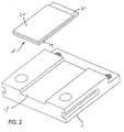
- the top surface of the baseplate 1 with respect to Fig. 2 is formed with a recess 17 which is rectangular in cross-section and open at both ends.
- This recess 17 is intended to receive flush therein a piezoelectric member 18 which is constructed from a preferably ceramic support layer 19 and a plate 20 of piezoelectric material stuck to the top surface thereof. That surface of the plate 19 which faces the plate 20 is covered with a thin metal layer 21.
- the construction is such that the plate 19 projects from the plate 20 at one end.
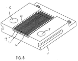
- the piezoelectric element 18 constructed in this way is fixed in the recess 17 of the baseplate 1, e.g. by gluing, in such manner that the coplanar ends of the plates 19 and 20 project inwards somewhat in the recess 17 with respect to the adjacent top surface of the plate 1 (Fig. 3).
- the length of the ceramic plate 19 is a little shorter than the length of the recess 17, so that the plate 19 is supported by the bottom surface of plate 17 over its entire length.
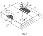
- the baseplate 3 is fixed in a suitable processing machine for the formation of a number of slots extending parallel to one another in the longitudinal direction of the piezoelectric member, through the plate 20 and over a short distance in the plate 19, in such manner that the plate 20 is divided into a large number of piezoelectric elements 23 separated from one another by slots or incisions 22.
- the incisions or slots 22 are made, at least one of the holes 5 in the baseplate 1 is used as a guide, such holes being accurately dimensioned and located and acting as a reference means for making the slots or gaps 22.
- this has a favourable effect on the assembly of the inkjet array, since said holes 5 in fact also form reference means for locating the ink duct plate 3 relatively to the baseplate 1.
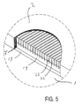
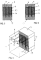
- the plastic covering layer 2 is applied, for example by so casting the plastic that it also penetrates into the incisions 22 in the plates 19 and 20 so that these incisions are filled with plastic separating strips 24 which separate the piezoelectric elements 23 from one another (Fig. 7).
- the facing sides of the piezoelectric elements 23 can be treated with a substance which prevents subsequent adhesion of the plastic material forming the separating strips 24 to the opposite wall parts of the piezoelectric elements 23.
- a layer of material covering the free top edges of the piezoelectric elements 23 can first be placed over the piezoelectric member, whereafter a suitable liquid, which, for example, leaves a thin Teflon layer on the facing sides of the piezoelectric elements 23, is passed through the gaps between the piezoelectric elements 23.
- the space formed near one end face of the baseplate 1 at that end of the piezoelectric member which recedes slightly with respect to the associated end face, is also filled with a plastic layer 2', it also being possible to ensure that this plastic projects initially slightly beyond the associated end face of the baseplate 1.
- the top surface of the covering layer 2 is also finished to be very accurately flat.
- the piezoelectric elements project slightly beyond the covering plate 2. Those ends of the piezoelectric elements 23 which project from the covering plate 2 are interconnected by a conductor 25, which can be earthed by means of a cable 26 when the device is in use.
- the provision of the incisions 22 causes the plate 19 to be subdivided, at the metal layer 21 forming its top, into a large number of electrodes 27 each connected to one of the piezoelectric elements 23.
- a lead 28 for the supply of current is connected to each of these electrodes.
- a number of parallel ink ducts 4 are formed in that surface of the plate member 3 which faces the baseplate, i.e., in the bottom of the plate 3 in the position shown in Fig. 1.
- These ink ducts have a constant depth (+/- 10 to 100 ⁇ m deep, preferably 30 ⁇ m deep) over their entire length, and a constant rectangular cross-section over the major part of their length. Comparable results were also obtained with shallow ducts which were of decreasing depth towards one side. By means of these shallow ducts it is possible to increase the integration density (number of ducts per mm) without appreciably affecting the strength and life of the array.
- a piezoelectric element 23 extending parallel to the ink duct will be located opposite each ink duct 4 in the manner indicated in Figs. 7 to 9.
- This accurate alignment of the piezoelectric elements 23 (with a width of about 150 ⁇ m) with respect to the ink ducts 30 (with a width of about 200 ⁇ m) is achieved in a simple and efficient manner by the fact that the holes 5 and 6 in the plates 1 and 3 respectively, which ensure accurate positioning of the plates relatively to one another by means of locating bushes 8, are used as reference means for locating the incisions 22 and ink ducts 4 respectively.
- Control of the volume of an ink duct situated adjacent the ink duct opposite the piezoelectric element activated to eject an ink drop also appears to be considerably less than in the case of a rigid connection between the piezoelectric elements 23 and the separating strips 24 which separate the piezoelectric elements from one another.
- the above-described inkjet array is intended more particularly for use with ink which is solid at room temperature (hot-melt ink-jet system).
- a heating element (not shown) can be disposed for example beneath the baseplate 1. Since the plate 20 (Fig. 1) is divided into a number of completely separated piezoelectric elements 23 (Fig. 7) disposed on the ceramic support layer 19, the coefficient of expansion of the piezoelectric material on heating of the inkjet array will not cause the piezoelectric elements 23 to be displaced with respect to the plate 3 and hence arrive next to the ink ducts 4. This is the case particularly if the plate 3 is also made of ceramic material.
- a good effect at elevated temperature is also obtained with a plate 3 made from a metal or plastic having a coefficient of expansion which does not differ too much from that of the support layer 19. Since in such hot-melt ink-jet systems the melting temperature of the ink is generally between 60°C and 120°C, the plastic used for the separating strips 24 is also one which is resistant to such temperature.
Landscapes
- Engineering & Computer Science (AREA)
- Manufacturing & Machinery (AREA)
- Particle Formation And Scattering Control In Inkjet Printers (AREA)
Description
Claims (10)
- An inkjet array provided with a piezoelectric member (18) and a member (3) in the form of a plate opposite the same, its surface which faces the piezoelectric member being provided with a number of parallel elongated ink ducts (4), while the piezoelectric member (18) is provided with a number of elongated parallel piezoelectric elements (23) substantially rectangular in cross section, each piezoelectric element (23) being situated opposite an ink duct (4), whereby the piezoelectric member (18) has opposite sides substantially parallel to the elongated piezoelectric elements (23) and is received in a recess (17) in a baseplate (1) which faces the ink duct surface of the plate member (3) containing the ink ducts (4) and is fixed to said plate member (3), said recess having opposite side walls,
characterised in that
the piezoelectric member is received in the recess such that the said opposite sides of the piezoelectric member (18) are respectively flush with the opposite side walls of the recess. - An inkjet array according to claim 1, characterised in that the piezoelectric member (18) is constructed from a plate (19) on which are secured a number of parallel piezoelectric elements (23), the plate (19) projecting from the piezoelectric elements at one end and being provided at the top with electrodes each connected to a piezoelectric element.
- An inkjet array according to claim 1, characterised in that the piezoelectric elements (23) disposed on the plate (19) are interconnected while each of the electrodes on the plate is connected to a current supply line.
- An inkjet array according to claim 2 or 3, characterised in that the plate (19) is made from ceramic material.
- An inkjet array according to any one of the preceding claims, characterised in that there are provided in gaps (24) between the piezoelectric elements (23) separating strips which fill the gaps and which are detached from the piezoelectric elements.
- An inkjet array according to any one of the preceding claims, characterised in that the piezoelectric elements (23) and also the parts of the support plate (19) situated on either side of said piezoelectric elements are covered by a plastic covering layer.
- An inkjet array according to claim 6, characterised in that near one end the covering layer is provided with a projecting part received in the baseplate recess (7) and covering the piezoelectric member (18) at one end.
- An inkjet array according to any one of the preceding claims, characterised in that the ink ducts (4) have a constant depth over their entire length, have a constant rectangular cross section over the major part of their length, and gradually decrease in cross section near their ends to merge into a jet (31).
- An inkjet array according to any one of the preceding claims, characterised in that the baseplate (1) and the plate member (3) provided with ink ducts (4) are secured to one another by bolts (10, 15) screwed into locating bushes extending in bores (5, 6) formed in the baseplate (1) and in the plate member (3).
- An inkjet array according to any one of the preceding claims, characterised in that it is provided with a heating element by means of which ink solid at room temperature can be brought into the liquid state in the ink ducts during operation.
Applications Claiming Priority (2)
| Application Number | Priority Date | Filing Date | Title |
|---|---|---|---|
| NL9401698 | 1994-10-14 | ||
| NL9401698A NL9401698A (en) | 1994-10-14 | 1994-10-14 | Inkjet printhead and method of manufacturing an inkjet printhead. |
Publications (2)
| Publication Number | Publication Date |
|---|---|
| EP0706887A1 EP0706887A1 (en) | 1996-04-17 |
| EP0706887B1 true EP0706887B1 (en) | 1999-03-17 |
Family
ID=19864777
Family Applications (1)
| Application Number | Title | Priority Date | Filing Date |
|---|---|---|---|
| EP95202558A Expired - Lifetime EP0706887B1 (en) | 1994-10-14 | 1995-09-22 | Inkjet array and method of producing the same |
Country Status (5)
| Country | Link |
|---|---|
| US (1) | US5757404A (en) |
| EP (1) | EP0706887B1 (en) |
| JP (1) | JP2826810B2 (en) |
| DE (1) | DE69508333T2 (en) |
| NL (1) | NL9401698A (en) |
Cited By (1)
| Publication number | Priority date | Publication date | Assignee | Title |
|---|---|---|---|---|
| WO2012072114A1 (en) | 2010-11-30 | 2012-06-07 | Reinhardt Microtech Ag | Piezoelectric actuator for ink jet printing heads |
Families Citing this family (7)
| Publication number | Priority date | Publication date | Assignee | Title |
|---|---|---|---|---|
| DE69605641T2 (en) * | 1996-02-14 | 2000-06-08 | Oce-Technologies B.V., Venlo | Printhead for an inkjet printer |
| NL1004016C2 (en) * | 1996-09-12 | 1998-03-13 | Oce Tech Bv | Inkjet print head. |
| GB9626684D0 (en) * | 1996-12-23 | 1997-02-12 | Domino Printing Sciences Plc | Continuous inkjet printer |
| WO1999011461A1 (en) * | 1997-08-29 | 1999-03-11 | Topaz Technologies, Inc. | Integrated head assembly for an ink jet printer |
| JP3649634B2 (en) * | 1999-02-09 | 2005-05-18 | 東芝テック株式会社 | Inkjet printer head and manufacturing method thereof |
| JP2007076176A (en) * | 2005-09-14 | 2007-03-29 | Olympus Corp | High-density ink-jet head module |
| KR102157206B1 (en) * | 2018-12-20 | 2020-09-17 | 동의대학교 산학협력단 | Pneumatic dispenser without adhesion process and pneumatic printing system comprising the same |
Family Cites Families (12)
| Publication number | Priority date | Publication date | Assignee | Title |
|---|---|---|---|---|
| JPS6090770A (en) * | 1983-10-25 | 1985-05-21 | Seiko Epson Corp | Ink jet head |
| JP3073783B2 (en) * | 1990-04-06 | 2000-08-07 | 株式会社リコー | Inkjet head |
| JPH04241949A (en) * | 1991-01-14 | 1992-08-28 | Citizen Watch Co Ltd | Ink jet head |
| JPH04363250A (en) * | 1991-03-19 | 1992-12-16 | Tokyo Electric Co Ltd | Inkjet printer head and its manufacturing method |
| US5270740A (en) * | 1991-03-26 | 1993-12-14 | Ricoh Company, Ltd. | Ink jet head |
| JP3215147B2 (en) * | 1991-04-05 | 2001-10-02 | 株式会社リコー | Driving method of liquid jet recording head |
| JP3103404B2 (en) * | 1991-10-22 | 2000-10-30 | キヤノン株式会社 | Method for manufacturing inkjet recording head, inkjet recording head, and inkjet recording apparatus |
| JPH0664168A (en) * | 1992-03-11 | 1994-03-08 | Tokyo Electric Co Ltd | Ink jet printer head and manufacture thereof |
| DE4225799A1 (en) * | 1992-07-31 | 1994-02-03 | Francotyp Postalia Gmbh | Inkjet printhead and process for its manufacture |
| US5334415A (en) * | 1992-09-21 | 1994-08-02 | Compaq Computer Corporation | Method and apparatus for film coated passivation of ink channels in ink jet printhead |
| US5345256A (en) * | 1993-02-19 | 1994-09-06 | Compaq Computer Corporation | High density interconnect apparatus for an ink jet printhead |
| JP3468377B2 (en) * | 1993-03-01 | 2003-11-17 | セイコーエプソン株式会社 | Driving method of ink jet recording head, ink jet recording apparatus, and control apparatus of ink jet recording head |
-
1994
- 1994-10-14 NL NL9401698A patent/NL9401698A/en not_active Application Discontinuation
-
1995
- 1995-09-22 EP EP95202558A patent/EP0706887B1/en not_active Expired - Lifetime
- 1995-09-22 DE DE69508333T patent/DE69508333T2/en not_active Expired - Lifetime
- 1995-09-26 US US08/533,853 patent/US5757404A/en not_active Expired - Lifetime
- 1995-10-04 JP JP7282435A patent/JP2826810B2/en not_active Expired - Fee Related
Cited By (1)
| Publication number | Priority date | Publication date | Assignee | Title |
|---|---|---|---|---|
| WO2012072114A1 (en) | 2010-11-30 | 2012-06-07 | Reinhardt Microtech Ag | Piezoelectric actuator for ink jet printing heads |
Also Published As
| Publication number | Publication date |
|---|---|
| US5757404A (en) | 1998-05-26 |
| JPH08300651A (en) | 1996-11-19 |
| NL9401698A (en) | 1996-05-01 |
| EP0706887A1 (en) | 1996-04-17 |
| DE69508333D1 (en) | 1999-04-22 |
| JP2826810B2 (en) | 1998-11-18 |
| DE69508333T2 (en) | 1999-09-02 |
Similar Documents
| Publication | Publication Date | Title |
|---|---|---|
| EP0518380B1 (en) | On-demand type ink jet print head | |
| US6565193B1 (en) | Component for a four color printhead module | |
| US6039440A (en) | Ink-jet head | |
| AU661750B2 (en) | Liquid jet recording head and liquid jet recording apparatus having same | |
| EP0402172B1 (en) | Head for ink-jet printer | |
| US5535494A (en) | Method of fabricating a piezoelectric ink jet printhead assembly | |
| EP0578331A1 (en) | Method of filling an ink cartridge for ink jet recording apparatus | |
| EP1011977B1 (en) | Droplet deposition apparatus | |
| US8500249B2 (en) | Printhead module for an inkjet printhead assembly | |
| US20080291243A1 (en) | Ink jet print head, method for manufacturing ink jet print head, and printing apparatus | |
| JPH0448622B2 (en) | ||
| US5757404A (en) | Inkjet array and method of production | |
| EP0723866A1 (en) | Ink jet head, method for producing the same and method for driving the same | |
| WO2000026033A1 (en) | Droplet ejection apparatus | |
| KR20010082239A (en) | Droplet deposition apparatus | |
| US6350020B1 (en) | Ink jet recording head | |
| JP2858956B2 (en) | Ink jet head and method of manufacturing the same | |
| JP3683941B2 (en) | Ink jet head, ink jet cartridge having the head, and ink jet apparatus equipped with the head | |
| EP1022140A1 (en) | Inkjet printhead | |
| JP3058458B2 (en) | Ink jet recording head and ink jet recording apparatus | |
| AU2004200367B2 (en) | Inkjet Printhead with Flex PCB in Ink Flow Path | |
| JP3466827B2 (en) | Ink jet recording head and method for manufacturing the ink jet recording head | |
| JPH04250048A (en) | Inkjet recording head and inkjet recording device | |
| WO1999011461A1 (en) | Integrated head assembly for an ink jet printer | |
| AU2126701A (en) | Four color modular printhead assembly |
Legal Events
| Date | Code | Title | Description |
|---|---|---|---|
| PUAI | Public reference made under article 153(3) epc to a published international application that has entered the european phase |
Free format text: ORIGINAL CODE: 0009012 |
|
| AK | Designated contracting states |
Kind code of ref document: A1 Designated state(s): DE FR GB IT NL SE |
|
| 17P | Request for examination filed |
Effective date: 19961005 |
|
| 17Q | First examination report despatched |
Effective date: 19970512 |
|
| RAP1 | Party data changed (applicant data changed or rights of an application transferred) |
Owner name: OCE-TECHNOLOGIES B.V. |
|
| GRAG | Despatch of communication of intention to grant |
Free format text: ORIGINAL CODE: EPIDOS AGRA |
|
| GRAG | Despatch of communication of intention to grant |
Free format text: ORIGINAL CODE: EPIDOS AGRA |
|
| GRAG | Despatch of communication of intention to grant |
Free format text: ORIGINAL CODE: EPIDOS AGRA |
|
| GRAG | Despatch of communication of intention to grant |
Free format text: ORIGINAL CODE: EPIDOS AGRA |
|
| GRAH | Despatch of communication of intention to grant a patent |
Free format text: ORIGINAL CODE: EPIDOS IGRA |
|
| GRAH | Despatch of communication of intention to grant a patent |
Free format text: ORIGINAL CODE: EPIDOS IGRA |
|
| GRAA | (expected) grant |
Free format text: ORIGINAL CODE: 0009210 |
|
| AK | Designated contracting states |
Kind code of ref document: B1 Designated state(s): DE FR GB IT NL SE |
|
| REF | Corresponds to: |
Ref document number: 69508333 Country of ref document: DE Date of ref document: 19990422 |
|
| ITF | It: translation for a ep patent filed | ||
| ET | Fr: translation filed | ||
| PLBE | No opposition filed within time limit |
Free format text: ORIGINAL CODE: 0009261 |
|
| STAA | Information on the status of an ep patent application or granted ep patent |
Free format text: STATUS: NO OPPOSITION FILED WITHIN TIME LIMIT |
|
| 26N | No opposition filed | ||
| REG | Reference to a national code |
Ref country code: GB Ref legal event code: IF02 |
|
| PGFP | Annual fee paid to national office [announced via postgrant information from national office to epo] |
Ref country code: SE Payment date: 20030819 Year of fee payment: 9 |
|
| PG25 | Lapsed in a contracting state [announced via postgrant information from national office to epo] |
Ref country code: SE Free format text: LAPSE BECAUSE OF NON-PAYMENT OF DUE FEES Effective date: 20040923 |
|
| EUG | Se: european patent has lapsed | ||
| PG25 | Lapsed in a contracting state [announced via postgrant information from national office to epo] |
Ref country code: IT Free format text: LAPSE BECAUSE OF NON-PAYMENT OF DUE FEES;WARNING: LAPSES OF ITALIAN PATENTS WITH EFFECTIVE DATE BEFORE 2007 MAY HAVE OCCURRED AT ANY TIME BEFORE 2007. THE CORRECT EFFECTIVE DATE MAY BE DIFFERENT FROM THE ONE RECORDED. Effective date: 20050922 |
|
| PGFP | Annual fee paid to national office [announced via postgrant information from national office to epo] |
Ref country code: GB Payment date: 20120920 Year of fee payment: 18 |
|
| PGFP | Annual fee paid to national office [announced via postgrant information from national office to epo] |
Ref country code: DE Payment date: 20120921 Year of fee payment: 18 |
|
| PGFP | Annual fee paid to national office [announced via postgrant information from national office to epo] |
Ref country code: FR Payment date: 20121010 Year of fee payment: 18 |
|
| PGFP | Annual fee paid to national office [announced via postgrant information from national office to epo] |
Ref country code: NL Payment date: 20120921 Year of fee payment: 18 |
|
| REG | Reference to a national code |
Ref country code: NL Ref legal event code: V1 Effective date: 20140401 |
|
| GBPC | Gb: european patent ceased through non-payment of renewal fee |
Effective date: 20130922 |
|
| REG | Reference to a national code |
Ref country code: FR Ref legal event code: ST Effective date: 20140530 |
|
| REG | Reference to a national code |
Ref country code: DE Ref legal event code: R119 Ref document number: 69508333 Country of ref document: DE Effective date: 20140401 |
|
| PG25 | Lapsed in a contracting state [announced via postgrant information from national office to epo] |
Ref country code: GB Free format text: LAPSE BECAUSE OF NON-PAYMENT OF DUE FEES Effective date: 20130922 |
|
| PG25 | Lapsed in a contracting state [announced via postgrant information from national office to epo] |
Ref country code: NL Free format text: LAPSE BECAUSE OF NON-PAYMENT OF DUE FEES Effective date: 20140401 Ref country code: DE Free format text: LAPSE BECAUSE OF NON-PAYMENT OF DUE FEES Effective date: 20140401 Ref country code: FR Free format text: LAPSE BECAUSE OF NON-PAYMENT OF DUE FEES Effective date: 20130930 |