EP0706313B1 - Connector for a substrate with an electronic circuit - Google Patents
Connector for a substrate with an electronic circuit Download PDFInfo
- Publication number
- EP0706313B1 EP0706313B1 EP95202606A EP95202606A EP0706313B1 EP 0706313 B1 EP0706313 B1 EP 0706313B1 EP 95202606 A EP95202606 A EP 95202606A EP 95202606 A EP95202606 A EP 95202606A EP 0706313 B1 EP0706313 B1 EP 0706313B1
- Authority
- EP
- European Patent Office
- Prior art keywords
- housing
- reference plate
- substrate
- contact
- circuit board
- Prior art date
- Legal status (The legal status is an assumption and is not a legal conclusion. Google has not performed a legal analysis and makes no representation as to the accuracy of the status listed.)
- Expired - Lifetime
Links
- 239000000758 substrate Substances 0.000 title claims description 37
- 230000008878 coupling Effects 0.000 claims description 5
- 238000010168 coupling process Methods 0.000 claims description 5
- 238000005859 coupling reaction Methods 0.000 claims description 5
- 239000011810 insulating material Substances 0.000 claims description 4
- 101000726081 Mus musculus Cysteine-rich secretory protein 3 Proteins 0.000 description 9
- 238000010276 construction Methods 0.000 description 1
Images


Classifications
-
- H—ELECTRICITY
- H05—ELECTRIC TECHNIQUES NOT OTHERWISE PROVIDED FOR
- H05K—PRINTED CIRCUITS; CASINGS OR CONSTRUCTIONAL DETAILS OF ELECTRIC APPARATUS; MANUFACTURE OF ASSEMBLAGES OF ELECTRICAL COMPONENTS
- H05K7/00—Constructional details common to different types of electric apparatus
- H05K7/02—Arrangements of circuit components or wiring on supporting structure
- H05K7/10—Plug-in assemblages of components, e.g. IC sockets
- H05K7/1053—Plug-in assemblages of components, e.g. IC sockets having interior leads
- H05K7/1061—Plug-in assemblages of components, e.g. IC sockets having interior leads co-operating by abutting
- H05K7/1069—Plug-in assemblages of components, e.g. IC sockets having interior leads co-operating by abutting with spring contact pieces
Definitions
- the invention relates to a connector for connecting a substrate with an electronic circuit to a printed circuit board, wherein a main surface of the substrate is provided with contact balls arranged in a given grid pattern with a predetermined pitch in column and row directions and the printed circuit board is provided with contact pads arranged in said grid pattern, said connector comprising a housing of insulating material with a zone for receiving said substrate, wherein through-holes are provided in said zone in said grid pattern and contact members are provided in at least a part of said through-holes for interconnecting corresponding contact balls of the substrate and contact pads of the printed circuit board, and positioning means for locating the substrate with respect to the housing in such a manner that the through-holes of the housing are aligned with the contact balls of the substrate.
- a connector of this type is described for example in US-A-4,969,826 and US-A-4,699,593. Such connectors are used for example for connecting the contact pads of the substrate to the contact pads of the printed circuit board.
- the contact pads are arranged in a grid pattern of 32 x 32. At this an accurate positioning of the substrate with respect to the housing and of the housing with respect to the printed circuit board is very important.
- the construction of the known connector is relatively complicated and further the connector is only suitable for a substrate of one size.
- EP-A-0 619 696 which falls within the terms of Article 54(3) EPC discloses a connector for connecting a substrate with an electronic circuit to a printed circuit board.
- the invention aims to provide a connector of this type wherein the positioning means are made in a simple manner and allow for an accurate positioning of the substrate with respect to the contact members of the housing while the connector is further suitable for substrates of different sizes.
- said positioning means comprises at least one reference plate which can be positioned on the housing, said reference plate comprising through-holes arranged in said grid pattern for receiving at least a part of the contact balls of the substrate, wherein each reference plate and the housing are provided with cooperating coupling means for accurately positioning the reference plate with respect to the housing.
- the reference plate shows the important advantage that substrates of different sizes can be positioned on the housing of the connector. Because the reference plate is made as a separate component, reference plates with different sizes can be provided so that the connector is suitable for substrates of various sizes.
- each reference plate is provided with reference marks for indicating the correct position of substrates of different sizes.
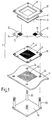
- Fig. 1 shows an exploded view of an embodiment of the connector according to the invention, wherein a substrate, a part of a printed circuit board and the mounting means are also shown.
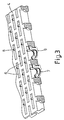
- Fig. 2 partly shows a cross-section of the connector of fig. 1 in assembled position.
- Fig. 3 partly shows a cross-section of the housing of the connector of fig. 1 at a larger scale.
- Fig. 4 partly shows a top view of the connector of fig. 1 at a larger scale.
- Fig. 5 is a perspective view of the bottom side of the reference plate of the connector of fig. 1.
- Fig. 1 shows an exploded view of a connector 1 for a substrate 2 with an electronic circuit.
- the substrate 2 is made as a so-called single chip package (SCP) of which the bottom main surface is provided with a large number of contact balls 3 which are arranged in a given grid pattern with a predetermined pitch in column and row directions of for example 1.27 mm.
- the contact balls 3 could for example be arranged in an array of 32 x 32.
- the connector 1 is provided with a housing 4 of insulating material with a zone 5 for receiving the SCP 2. As shown in fig. 3 at a larger scale, through-holes 6 are provided in the zone 5 of the housing 4 in the same pattern as the contact balls of the SCP 2.
- a contact member 7 is mounted in each hole 6, a contact part 8 of the contact member 7 being adapted to contact a contact ball 3 and a contact part 9 being adapted to contact a contact pad 10 of a printed circuit board 11.
- These contact pads 10 of the printed circuit board 11 are of course arranged in the same pattern as the contact balls 3.
- the connector 1 comprises two reference plates 12 made of insulating material, each reference plate being provided with through-holes 13 as clearly shown in the top view of fig. 4.
- the holes 13 are arranged according to the same pattern as the contact balls 3 and are accurately located above the holes 6 at the location of the contact parts 8 when the reference plate is located on the housing 4.
- each reference plate 12 is substantially smaller than the surface of the housing 4 so that only a part of the zone 5 is overlapped and holes 13 are provided for only a part of the contact balls 3.
- the thickness of the reference plates 12 is such that the contact balls of the SCP 2 can contact the contact parts 8 of the contact members 7 through the holes 13.
- Each reference plate 12 can be positioned accurately with respect to the housing 4, in that each reference plate 12 is coupled with the housing 4 by means of a hollow pin at the bottom side and a projection 15 shown in fig. 5.
- the housing 4 comprises at each corner an opening 16 in which the hollow pin 14 can be fittingly received and a slotted hole 17 for the projection 15. Because the hollow pin 14 and the projection 15, and the opening 16 and the slotted hole 17, respectively, are accurately located with respect to the holes 13 and the holes 6, respectively, each reference plate 12 can be positioned accurately on the housing 4 by means of these cooperating coupling means 14-17.
- the SCP 2 can be placed easily in the correct position on the zone 5 of the housing 4.
- the reference plates described show the advantage that positioning of the SCP 2 with respect to the holes 6 in the zone 5 occurs by using the contact balls 3 of the SCP 2 themselves.
- the reference plates are suitable for substrates of different sizes.
- reference marks 18 are provided on the top side of each reference plate 12 by means of which substrates of different sizes can be placed on the same reference plate. Further reference plates of different sizes can be combined with the same housing 4.
- the housing 4 is also suitable for substrates of different sizes. If the substrate 2 is smaller than the zone 5 of the housing 4 it is possible to provide contact members 7 only in the holes 6 which will be lying opposite of contact balls 3 of the respective substrate 2, if desired.
- Fig. 2 shows the connector 1 in assembled position. Attaching the substrate on the connector 1 and attaching the connector 1 on the printed circuit board 11, respectively, occurs by means of a mounting plate 19 with four mounting bolts 20 and a mounting frame 21 which is put on the mounting bolts 20 with openings 22. By means of nuts 23 the assembly is attached.
- Fig. 2 shows that the mounting bolt 20 extends through the hollow pin 14 of the reference plate 12 at the corresponding corner. This means that besides the openings for mounting the assembly no further openings need to be provided for positioning the reference plates 12 on the housing 4.
- Fig. 2 further shows that the pin 14 of the reference plate 12 projects through the housing 4 and is fittingly received in an opening 24 of the printed circuit board 11. These openings 24 are accurately located with respect to the contact pads 10 of the printed circuit board 11. In this manner the pin 14 of each reference plate 12 provides also for a positioning of the housing 4 with respect to the contact pads 10 of the printed circuit board 11.
- two reference plates 12 are provided diametrically opposed with respect to the zone 5 of the housing 4. It is however also possible to use only one or more than two reference plates.
Landscapes
- Engineering & Computer Science (AREA)
- Microelectronics & Electronic Packaging (AREA)
- Coupling Device And Connection With Printed Circuit (AREA)
- Multi-Conductor Connections (AREA)
Description
-
- The invention relates to a connector for connecting a substrate with an electronic circuit to a printed circuit board, wherein a main surface of the substrate is provided with contact balls arranged in a given grid pattern with a predetermined pitch in column and row directions and the printed circuit board is provided with contact pads arranged in said grid pattern, said connector comprising a housing of insulating material with a zone for receiving said substrate, wherein through-holes are provided in said zone in said grid pattern and contact members are provided in at least a part of said through-holes for interconnecting corresponding contact balls of the substrate and contact pads of the printed circuit board, and positioning means for locating the substrate with respect to the housing in such a manner that the through-holes of the housing are aligned with the contact balls of the substrate.
- A connector of this type is described for example in US-A-4,969,826 and US-A-4,699,593. Such connectors are used for example for connecting the contact pads of the substrate to the contact pads of the printed circuit board. In a known substrate the contact pads are arranged in a grid pattern of 32 x 32. At this an accurate positioning of the substrate with respect to the housing and of the housing with respect to the printed circuit board is very important. The construction of the known connector is relatively complicated and further the connector is only suitable for a substrate of one size.
- EP-A-0 619 696 which falls within the terms of Article 54(3) EPC discloses a connector for connecting a substrate with an electronic circuit to a printed circuit board.
- The invention aims to provide a connector of this type wherein the positioning means are made in a simple manner and allow for an accurate positioning of the substrate with respect to the contact members of the housing while the connector is further suitable for substrates of different sizes.
- To this end the connector according to the invention said positioning means comprises at least one reference plate which can be positioned on the housing, said reference plate comprising through-holes arranged in said grid pattern for receiving at least a part of the contact balls of the substrate, wherein each reference plate and the housing are provided with cooperating coupling means for accurately positioning the reference plate with respect to the housing.
- In this manner a very simple positioning means is obtained by means of which the substrate can be positioned with respect to the contact members of the housing in a very accurate manner. The reference plate shows the important advantage that substrates of different sizes can be positioned on the housing of the connector. Because the reference plate is made as a separate component, reference plates with different sizes can be provided so that the connector is suitable for substrates of various sizes.
- In order to provide for an easy locating of substrate of different sizes on a reference plate, in a preferred embodiment, the upper side of each reference plate is provided with reference marks for indicating the correct position of substrates of different sizes.
- The invention will be further explained hereinafter by reference to the drawings, in which an embodiment of the connector according to the invention is shown.
- Fig. 1 shows an exploded view of an embodiment of the connector according to the invention, wherein a substrate, a part of a printed circuit board and the mounting means are also shown.
- Fig. 2 partly shows a cross-section of the connector of fig. 1 in assembled position.
- Fig. 3 partly shows a cross-section of the housing of the connector of fig. 1 at a larger scale.
- Fig. 4 partly shows a top view of the connector of fig. 1 at a larger scale.
- Fig. 5 is a perspective view of the bottom side of the reference plate of the connector of fig. 1.
- Fig. 1 shows an exploded view of a
connector 1 for asubstrate 2 with an electronic circuit. Thesubstrate 2 is made as a so-called single chip package (SCP) of which the bottom main surface is provided with a large number ofcontact balls 3 which are arranged in a given grid pattern with a predetermined pitch in column and row directions of for example 1.27 mm. Thecontact balls 3 could for example be arranged in an array of 32 x 32. - The
connector 1 is provided with ahousing 4 of insulating material with a zone 5 for receiving theSCP 2. As shown in fig. 3 at a larger scale, through-holes 6 are provided in the zone 5 of thehousing 4 in the same pattern as the contact balls of theSCP 2. Acontact member 7 is mounted in eachhole 6, a contact part 8 of thecontact member 7 being adapted to contact acontact ball 3 and a contact part 9 being adapted to contact acontact pad 10 of a printedcircuit board 11. Thesecontact pads 10 of the printedcircuit board 11 are of course arranged in the same pattern as thecontact balls 3. - In order to obtain good connections between the
contact balls 3 of theSCP 2 and thecontact pads 10 of the printedcircuit board 11 it is of course very important that theSCP 2 is positioned accurately with respect to theopenings 6 in thehousing 4 in such a manner that thecontact balls 3 of theSCP 2 contact with certainty the contact parts 8 of thecontact members 7 located in theopenings 6. To this end theconnector 1 comprises tworeference plates 12 made of insulating material, each reference plate being provided with through-holes 13 as clearly shown in the top view of fig. 4. Theholes 13 are arranged according to the same pattern as thecontact balls 3 and are accurately located above theholes 6 at the location of the contact parts 8 when the reference plate is located on thehousing 4. The surface of eachreference plate 12 is substantially smaller than the surface of thehousing 4 so that only a part of the zone 5 is overlapped andholes 13 are provided for only a part of thecontact balls 3. The thickness of thereference plates 12 is such that the contact balls of theSCP 2 can contact the contact parts 8 of thecontact members 7 through theholes 13. - Each
reference plate 12 can be positioned accurately with respect to thehousing 4, in that eachreference plate 12 is coupled with thehousing 4 by means of a hollow pin at the bottom side and aprojection 15 shown in fig. 5. Thehousing 4 comprises at each corner an opening 16 in which thehollow pin 14 can be fittingly received and a slottedhole 17 for theprojection 15. Because thehollow pin 14 and theprojection 15, and the opening 16 and theslotted hole 17, respectively, are accurately located with respect to theholes 13 and theholes 6, respectively, eachreference plate 12 can be positioned accurately on thehousing 4 by means of these cooperating coupling means 14-17. - When the
reference plates 12 are mounted on thehousing 4, theSCP 2 can be placed easily in the correct position on the zone 5 of thehousing 4. The reference plates described show the advantage that positioning of theSCP 2 with respect to theholes 6 in the zone 5 occurs by using thecontact balls 3 of theSCP 2 themselves. Moreover the reference plates are suitable for substrates of different sizes. As indicated in the top view of fig. 4reference marks 18 are provided on the top side of eachreference plate 12 by means of which substrates of different sizes can be placed on the same reference plate. Further reference plates of different sizes can be combined with thesame housing 4. Thehousing 4 is also suitable for substrates of different sizes. If thesubstrate 2 is smaller than the zone 5 of thehousing 4 it is possible to providecontact members 7 only in theholes 6 which will be lying opposite ofcontact balls 3 of therespective substrate 2, if desired. - Fig. 2 shows the
connector 1 in assembled position. Attaching the substrate on theconnector 1 and attaching theconnector 1 on the printedcircuit board 11, respectively, occurs by means of amounting plate 19 with fourmounting bolts 20 and amounting frame 21 which is put on themounting bolts 20 withopenings 22. By means ofnuts 23 the assembly is attached. Fig. 2 shows that themounting bolt 20 extends through thehollow pin 14 of thereference plate 12 at the corresponding corner. This means that besides the openings for mounting the assembly no further openings need to be provided for positioning thereference plates 12 on thehousing 4. - Fig. 2 further shows that the
pin 14 of thereference plate 12 projects through thehousing 4 and is fittingly received in an opening 24 of the printedcircuit board 11. Theseopenings 24 are accurately located with respect to thecontact pads 10 of the printedcircuit board 11. In this manner thepin 14 of eachreference plate 12 provides also for a positioning of thehousing 4 with respect to thecontact pads 10 of the printedcircuit board 11. - In the embodiment described two
reference plates 12 are provided diametrically opposed with respect to the zone 5 of thehousing 4. It is however also possible to use only one or more than two reference plates. - The invention is not restricted to the above-described embodiment which can be varied in a number of ways within the scope of the claims.
Claims (8)
- Connector (1) for connecting a substrate (2) with an electronic circuit to a printed circuit board (11), wherein a main surface of the substrate is provided with contact balls (3) arranged in a given grid pattern with a predetermined pitch in column and row directions and the printed circuit board is provided with contact pads (10) arranged in said grid pattern, said connector comprising a housing (4) of insulating material with a zone (5) for receiving said substrate, wherein through-holes (6) are provided in said zone in said grid pattern and contact members (7) are provided in at least a part of said through-holes for interconnecting corresponding contact balls of the substrate and contact pads of the printed circuit board, and positioning means for locating the substrate with respect to the housing in such a manner that the through-holes of the housing are aligned with the contact balls of the substrate, said positioning means comprises at least one reference plate (12) which can be positioned on the housing (4), said reference plate comprising through-holes (13) arranged in said grid pattern for receiving at least a part of the contact balls (3) of the substrate (2), wherein each reference plate and the housing are provided with cooperating coupling means (14-17) for accurately positioning the reference plate with respect to the housing.
- Connector according to claim 1, wherein the coupling means (14-17) of each reference plate (12) also provide a positioning of the housing (4) with respect to the contact pads (10) of the printed circuit board (11).
- Connector according to claim 1 or 2, wherein said coupling means (14-17) comprises a pin (14) formed at the lower side of each reference plate (12) and a through-hole (16) formed in the housing (4) in which said pin can be fittingly received, said pin and opening being located at an accurately predetermined location with respect to the corresponding through-holes (13) for the contact balls (3) and the contact members (7), respectively.
- Connector according to claim 2 and 3, wherein the pin (14) of each reference plate (12) projects through the opening (16) of the housing (4) and can be fittingly received in an opening (24) of the printed circuit board (11), which is located at an accurately predetermined location with respect to the contact pads (10) of the printed circuit board (11).
- Connector according to claim 2, 3 or 4, wherein the pin (14) of each reference plate (12) is hollow for receiving a mounting bolt (20).
- Connector according to anyone of claims 2-5, wherein each reference plate (12) comprises a projection (15) at its lower side cooperating with a corresponding opening (17) in said housing (4).
- Connector according to anyone of the preceding claims, wherein the upper side of each reference plate (12) is provided with reference marks (18) for indicating the correct position of substrates (2) with different sizes.
- Connector according to anyone of the preceding claims, including two reference plates (12) which can be positioned diametrically with respect to said zone (5) of the housing (4).
Applications Claiming Priority (2)
| Application Number | Priority Date | Filing Date | Title |
|---|---|---|---|
| NL9401657 | 1994-10-07 | ||
| NL9401657A NL9401657A (en) | 1994-10-07 | 1994-10-07 | Connector for a substrate with an electronic circuit. |
Publications (2)
| Publication Number | Publication Date |
|---|---|
| EP0706313A1 EP0706313A1 (en) | 1996-04-10 |
| EP0706313B1 true EP0706313B1 (en) | 1999-04-14 |
Family
ID=19864750
Family Applications (1)
| Application Number | Title | Priority Date | Filing Date |
|---|---|---|---|
| EP95202606A Expired - Lifetime EP0706313B1 (en) | 1994-10-07 | 1995-09-28 | Connector for a substrate with an electronic circuit |
Country Status (4)
| Country | Link |
|---|---|
| US (1) | US5628636A (en) |
| EP (1) | EP0706313B1 (en) |
| DE (1) | DE69509032T2 (en) |
| NL (1) | NL9401657A (en) |
Families Citing this family (8)
| Publication number | Priority date | Publication date | Assignee | Title |
|---|---|---|---|---|
| US5829988A (en) * | 1996-11-14 | 1998-11-03 | Amkor Electronics, Inc. | Socket assembly for integrated circuit chip carrier package |
| US6198630B1 (en) * | 1999-01-20 | 2001-03-06 | Hewlett-Packard Company | Method and apparatus for electrical and mechanical attachment, and electromagnetic interference and thermal management of high speed, high density VLSI modules |
| US6398558B1 (en) | 1999-08-04 | 2002-06-04 | Fci Americas Technology, Inc. | Electrical connector and contact therefor |
| US6848942B1 (en) | 2000-01-12 | 2005-02-01 | Molex Incorporated | Connectors having supportive barrier components |
| FR2826230B1 (en) | 2001-06-19 | 2003-11-07 | Bull Sa | DEVICE AND METHOD FOR FIXING INTEGRATED CIRCUITS ON A PRINTED CIRCUIT BOARD |
| US20070054514A1 (en) * | 2005-08-31 | 2007-03-08 | International Business Machines Corporation | Socket measurement apparatus and method |
| US7435099B2 (en) | 2006-12-21 | 2008-10-14 | Cinch Connectors, Inc. | Electrical connector and packaging assembly |
| CN102544884B (en) * | 2011-12-23 | 2015-04-01 | 富士康(昆山)电脑接插件有限公司 | Electric connector, electric connector casing and surface treatment method of electric connector casing |
Family Cites Families (6)
| Publication number | Priority date | Publication date | Assignee | Title |
|---|---|---|---|---|
| US4699593A (en) * | 1986-01-14 | 1987-10-13 | Amp Incorporated | Connector having contact modules for a substrate such as an IC chip carrier |
| US4957800A (en) * | 1989-06-27 | 1990-09-18 | Amp Incorporated | Method of constructing a monolithic block having an internal geometry and the block resulting therefrom |
| US4969826A (en) * | 1989-12-06 | 1990-11-13 | Amp Incorporated | High density connector for an IC chip carrier |
| US5247250A (en) * | 1992-03-27 | 1993-09-21 | Minnesota Mining And Manufacturing Company | Integrated circuit test socket |
| US5232372A (en) * | 1992-05-11 | 1993-08-03 | Amp Incorporated | Land grid array connector and method of manufacture |
| FR2703839B1 (en) * | 1993-04-09 | 1995-07-07 | Framatome Connectors France | Intermediate connector between printed circuit board and electronic circuit substrate. |
-
1994
- 1994-10-07 NL NL9401657A patent/NL9401657A/en not_active Application Discontinuation
-
1995
- 1995-09-28 EP EP95202606A patent/EP0706313B1/en not_active Expired - Lifetime
- 1995-09-28 DE DE69509032T patent/DE69509032T2/en not_active Expired - Fee Related
- 1995-10-05 US US08/539,485 patent/US5628636A/en not_active Expired - Fee Related
Also Published As
| Publication number | Publication date |
|---|---|
| DE69509032D1 (en) | 1999-05-20 |
| NL9401657A (en) | 1996-05-01 |
| EP0706313A1 (en) | 1996-04-10 |
| DE69509032T2 (en) | 1999-08-12 |
| US5628636A (en) | 1997-05-13 |
Similar Documents
| Publication | Publication Date | Title |
|---|---|---|
| EP0706312B1 (en) | Connector for a substrate with an electronic circuit | |
| US6278284B1 (en) | Testing IC socket | |
| US5746608A (en) | Surface mount socket for an electronic package, and contact for use therewith | |
| US7033184B2 (en) | Electrical interconnect device incorporating anisotropically conductive elastomer and flexible circuit | |
| US6442045B1 (en) | Stake attached contact assembly in an integrated circuit socket assembly | |
| US6181567B1 (en) | Method and apparatus for securing an electronic package to a circuit board | |
| US6097609A (en) | Direct BGA socket | |
| US5892245A (en) | Ball grid array package emulator | |
| US5131852A (en) | Electrical socket | |
| EP0838101B1 (en) | Electrical connectors | |
| IE902302L (en) | Header device | |
| WO2003030255A3 (en) | Multiple die interconnect system | |
| EP0706313B1 (en) | Connector for a substrate with an electronic circuit | |
| EP1143776A4 (en) | PRINTED CIRCUIT BOARD AND METHOD FOR MANUFACTURING THE SAME | |
| US6078505A (en) | Circuit board assembly method | |
| KR100730275B1 (en) | Electrical connector and method of making thereof | |
| WO1997000537A1 (en) | Flexible leads for tape ball grid array circuit | |
| US6123551A (en) | Electronic circuit interconnection method and apparatus | |
| DE60116437T2 (en) | Socket for BGA packages | |
| US5258890A (en) | Device for connecting the connection pins of an integrated circuit mounted in a dual-in-line (DIL) package to printed circuitry on a printed circuit board in n different ways | |
| TW345797B (en) | Plastic ball grid array module | |
| US6191369B1 (en) | Printed circuit board having a marker trace for component alignment | |
| JP2976326B2 (en) | Contact for BGA | |
| JPH0347270Y2 (en) | ||
| JP3376959B2 (en) | IC socket |
Legal Events
| Date | Code | Title | Description |
|---|---|---|---|
| PUAI | Public reference made under article 153(3) epc to a published international application that has entered the european phase |
Free format text: ORIGINAL CODE: 0009012 |
|
| AK | Designated contracting states |
Kind code of ref document: A1 Designated state(s): BE DE FR NL SE |
|
| 17P | Request for examination filed |
Effective date: 19960627 |
|
| 17Q | First examination report despatched |
Effective date: 19970708 |
|
| GRAG | Despatch of communication of intention to grant |
Free format text: ORIGINAL CODE: EPIDOS AGRA |
|
| GRAG | Despatch of communication of intention to grant |
Free format text: ORIGINAL CODE: EPIDOS AGRA |
|
| GRAH | Despatch of communication of intention to grant a patent |
Free format text: ORIGINAL CODE: EPIDOS IGRA |
|
| GRAH | Despatch of communication of intention to grant a patent |
Free format text: ORIGINAL CODE: EPIDOS IGRA |
|
| GRAA | (expected) grant |
Free format text: ORIGINAL CODE: 0009210 |
|
| AK | Designated contracting states |
Kind code of ref document: B1 Designated state(s): BE DE FR NL SE |
|
| REF | Corresponds to: |
Ref document number: 69509032 Country of ref document: DE Date of ref document: 19990520 |
|
| ET | Fr: translation filed | ||
| PLBE | No opposition filed within time limit |
Free format text: ORIGINAL CODE: 0009261 |
|
| STAA | Information on the status of an ep patent application or granted ep patent |
Free format text: STATUS: NO OPPOSITION FILED WITHIN TIME LIMIT |
|
| 26N | No opposition filed | ||
| PGFP | Annual fee paid to national office [announced via postgrant information from national office to epo] |
Ref country code: BE Payment date: 20040915 Year of fee payment: 10 |
|
| PGFP | Annual fee paid to national office [announced via postgrant information from national office to epo] |
Ref country code: SE Payment date: 20040917 Year of fee payment: 10 |
|
| PGFP | Annual fee paid to national office [announced via postgrant information from national office to epo] |
Ref country code: NL Payment date: 20040929 Year of fee payment: 10 Ref country code: FR Payment date: 20040929 Year of fee payment: 10 |
|
| PGFP | Annual fee paid to national office [announced via postgrant information from national office to epo] |
Ref country code: DE Payment date: 20041129 Year of fee payment: 10 |
|
| PG25 | Lapsed in a contracting state [announced via postgrant information from national office to epo] |
Ref country code: SE Free format text: LAPSE BECAUSE OF NON-PAYMENT OF DUE FEES Effective date: 20050929 |
|
| PG25 | Lapsed in a contracting state [announced via postgrant information from national office to epo] |
Ref country code: BE Free format text: LAPSE BECAUSE OF NON-PAYMENT OF DUE FEES Effective date: 20050930 |
|
| PG25 | Lapsed in a contracting state [announced via postgrant information from national office to epo] |
Ref country code: NL Free format text: LAPSE BECAUSE OF NON-PAYMENT OF DUE FEES Effective date: 20060401 Ref country code: DE Free format text: LAPSE BECAUSE OF NON-PAYMENT OF DUE FEES Effective date: 20060401 |
|
| EUG | Se: european patent has lapsed | ||
| PG25 | Lapsed in a contracting state [announced via postgrant information from national office to epo] |
Ref country code: FR Free format text: LAPSE BECAUSE OF NON-PAYMENT OF DUE FEES Effective date: 20060531 |
|
| NLV4 | Nl: lapsed or anulled due to non-payment of the annual fee |
Effective date: 20060401 |
|
| REG | Reference to a national code |
Ref country code: FR Ref legal event code: ST Effective date: 20060531 |
|
| BERE | Be: lapsed |
Owner name: *FRAMATOME CONNECTORS INTERNATIONAL Effective date: 20050930 |