EP0706230B1 - Radio frequency filter comprising helix resonators - Google Patents
Radio frequency filter comprising helix resonators Download PDFInfo
- Publication number
- EP0706230B1 EP0706230B1 EP95307092A EP95307092A EP0706230B1 EP 0706230 B1 EP0706230 B1 EP 0706230B1 EP 95307092 A EP95307092 A EP 95307092A EP 95307092 A EP95307092 A EP 95307092A EP 0706230 B1 EP0706230 B1 EP 0706230B1
- Authority
- EP
- European Patent Office
- Prior art keywords
- resonators
- resonator
- helix
- coupling
- insulating plate
- Prior art date
- Legal status (The legal status is an assumption and is not a legal conclusion. Google has not performed a legal analysis and makes no representation as to the accuracy of the status listed.)
- Expired - Lifetime
Links
- 230000008878 coupling Effects 0.000 claims description 59
- 238000010168 coupling process Methods 0.000 claims description 59
- 238000005859 coupling reaction Methods 0.000 claims description 59
- 229910052751 metal Inorganic materials 0.000 claims description 21
- 239000002184 metal Substances 0.000 claims description 21
- 239000004020 conductor Substances 0.000 claims description 17
- 238000010079 rubber tapping Methods 0.000 description 11
- 238000010276 construction Methods 0.000 description 10
- 239000003990 capacitor Substances 0.000 description 8
- 238000010586 diagram Methods 0.000 description 6
- 238000004519 manufacturing process Methods 0.000 description 6
- 230000005540 biological transmission Effects 0.000 description 4
- 238000011161 development Methods 0.000 description 4
- 238000012356 Product development Methods 0.000 description 3
- 238000000034 method Methods 0.000 description 3
- 239000011248 coating agent Substances 0.000 description 2
- 238000000576 coating method Methods 0.000 description 2
- 230000005684 electric field Effects 0.000 description 2
- 238000005476 soldering Methods 0.000 description 2
- 229910052782 aluminium Inorganic materials 0.000 description 1
- XAGFODPZIPBFFR-UHFFFAOYSA-N aluminium Chemical compound [Al] XAGFODPZIPBFFR-UHFFFAOYSA-N 0.000 description 1
- 230000008901 benefit Effects 0.000 description 1
- 230000008859 change Effects 0.000 description 1
- 230000003247 decreasing effect Effects 0.000 description 1
- 230000001934 delay Effects 0.000 description 1
- 230000005672 electromagnetic field Effects 0.000 description 1
- 239000011888 foil Substances 0.000 description 1
- 230000001939 inductive effect Effects 0.000 description 1
- 239000011810 insulating material Substances 0.000 description 1
- 230000004044 response Effects 0.000 description 1
- 230000007480 spreading Effects 0.000 description 1
Images



Classifications
-
- H—ELECTRICITY
- H01—ELECTRIC ELEMENTS
- H01P—WAVEGUIDES; RESONATORS, LINES, OR OTHER DEVICES OF THE WAVEGUIDE TYPE
- H01P1/00—Auxiliary devices
- H01P1/20—Frequency-selective devices, e.g. filters
- H01P1/201—Filters for transverse electromagnetic waves
- H01P1/205—Comb or interdigital filters; Cascaded coaxial cavities
Definitions
- the invention relates to a radio frequency filter which comprises at least two helix resonators disposed at a distance from each other, each of which is formed by a metal wire wound into a cylindrical coil.
- a filter comprising helix resonators is used widely in radio devices because of its good electrical properties and light structure.
- the resonator is a transmission line resonator and it is formed by a wire with a length of about a quarter of a wavelength wound into a cylindrical coil, which is placed in a grounded metal case.
- the characteristic impedance and accordingly the resonance frequency of the resonator are determined by physical dimensions of the cavity, by the ratio of the diameter of the helix coil to the inner dimension of the surrounding casing, and the distance between adjacent turns in the coil, i.e. the so called pitch, and the supporting structure possibly used for supporting the coil. Therefore producing a resonator with exactly a desired resonance frequency requires an accurate and uniform structure.
- a filter with desired properties can be built by cascading resonators and by arranging the coupling between them properly.
- the filters get smaller especially in portable radio devices the accuracy requirements in production and assembly grow considerably, because even small variations in the dimensions of the cavity, the cylindrical coil and the supporting structure have great influence on the resonance frequency.
- the filter When the filter is connected to an electrical circuit of a radio device its input and output ports must be matched with the circuit, i.e. the impedances from the ports to the filter must be the same as the impedances from the ports to the circuit to prevent reflections and transmission losses caused by sudden impedance changes.
- the resonators of the filters must be matched with each other if the signal is brought to the filter by physical connection to its helix coil.
- a suitable impedance level has to be found in the helix resonator, that is, a physical point of connection at which the impedance level of the resonator equals that of a device connected thereto or an adjacent resonator.
- the impedance level of the connection point is directly proportional to the electrical length between the point of connection and the short-circuited end of the resonator, whereby a lower or higher impedance level can be selected by moving the point of connection along the helix coil.
- This kind of matching is called tapping because the point of connection forms a tap point from the helix resonator.
- the tap connection point in the helix resonator can be determined by experimentation or by calculation using a calculated or measured characteristic impedance of the helix resonator, which is determined by the properties of the resonator. In many cases, the tap point in the helix resonator is made in its first turn.
- tapping has been made by soldering one end of a discrete coil or conductor to the wire forming the helix resonator at the tap point.
- the reproduction fidelity of such a tapping method has been found to be inadequate for series production.
- Inadequate accuracy in tapping results in a need for adjusting the tappings when tuning the filters, which increases tuning time and costs.
- a better tapping method has been presented in the Finnish patent 80542.
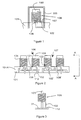
- the principle is shown in Figure 1.
- a helix resonator 106 has been placed around a projection 103 of a finger-like insulating plate 101 so that the projection is positioned inside the resonator coil, and thus supporting the coil.
- the end portion of the first turn of the coil 106 close to the insulating plate 101 is bent to form a straight portion 102 which is positioned tightly against the surface of the insulating plate over its entire length. This straight portion is called the leg of the resonator.
- the end 107 of the straight portion 102 is connected to the casing 105 and is short-circuited through it.
- a micro-strip 108 is provided on the circuit board at the foot of the projection 103 and is connected to the rest of the resonator circuit or forms a part of a more extensive microstrip pattern provided on the insulating plate.
- the direction of the microstrip is the same as the axis of the coil.
- the tapping point is thus the place where the microstrip 108 crosses the straight portion 102 of the coil.
- the strip and the straight portion are soldered together at this point.
- the tapping point and thus the desired impedance level are determined by moving the place of the microstrip 108 sideways.
- This method has the disadvantage of requiring several insulating plates which differ by the sideways position of the microstrip. This is a factor raising the expenses.
- Another disadvantage is that the tapping point cannot be fine tuned, because the leg must lie over the insulating plate. In practice, a leg lying over an insulating plate is not a very good solution, because a leg lying over an insulating plate with high losses increases the losses of the resonator.
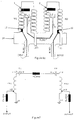
- FIG. 2 shows a part of a filter, which is surrounded by a casing, with four discrete helix resonator circuits - the resonators 106 and 107 have been referred to separately - each of which is mounted around finger-like projections 103 of a printed board 101. This is called a comb structure.
- An electrical circuit formed by strip lines 108 and 108' runs at the bottom 101A of the insulating plate 101, to which circuit one or several resonators, like resonator 106, have been electrically connected by soldering at the tap point 121.
- the tap point is in the first turn of the coil but it can as well be placed higher.
- This possibility is shown in Figure 102 by resonator 107 in which the tap point 122 is in the second turn of the coil.
- the microstrip protrudes little upwards on the finger-like projection and ends at the edge of it, whereto the turn of the resonator coil at that position is soldered.
- the tap point can thus be placed in any turn of the resonator coil and also several tap points can exist.
- the straight portion 102 of the resonator unlike the leg in Figure 1, is bent in parallel with the axis of the resonator and runs at a distance from the insulating plate and its other end is connected during the assembly phase to the bottom plate 31 of the casing.
- Figure 3 is grounded there through it if the plate is made of metal.
- the printed board of the radio device can also act as the bottom plate, at least one surface of which is coated with metal at the position of the filter, in which case the tip of the leg is connected to the metal coated surface.
- FIG. 4 shows an assembled filter according to the state of the art in which the filter casing is cut open to show the resonator more clearly.
- This filter has walls between the resonator circuits, the walls 42 and 43 of which are shown, and these walls can have coupling holes (not shown in the figure) through which the circuit can be coupled electromagnetically to an adjacent circuit.
- the separating wall and the way the insulating plate, which supports the resonators, is connected to the walls of the casing are not essential to the present invention.
- the casing 41 is usually extruded aluminum and the bottom plate 44 can be a metal plate or a printed board with one metal coated surface.
- the tap points 121 and 122 of the helix resonators 106 which are shown, are marked with a black dot, and from this tap point the resonator is electrically connected to the microstrip circuit (not seen in Figure) provided on the bottom part 101A of the insulating plate and on the fingers 103.
- the tips 112 and 113 of the legs 102 and 102' are soldered to the bottom plate 44, if it or its coating is metal, or they are galvanically connected to the metal coating on the other side of the bottom plate, if the bottom plate is a printed board.
- radio frequency filters which have at least two resonators
- traditional fixed capacitors which are suitable for relatively low frequency filters
- the values of the coupling capacitors become so low that traditional capacitors cannot be used, but instead, for instance a board capacitance implemented on the printed board must be utilized, in which the necessary capacitance is formed by metal foil coupling electrodes on each side of the insulating material.
- Helix filters described above and which have also been described e.g. in the US patents 4 977 383 and 5 047 739 the couplings between the resonators are accomplished usually so that the separating metal wall has a hole of a certain size through which the resonators are coupled electromagnetically to each other.
- Figure 5 shows a circuit diagram of a typical band-pass filter consisting of two resonators, e.g. helix resonators. Usually the resonators are coupled so, that a coupling hole has been made in the separating metal wall between the resonators through which the resonance circuits are coupled.
- the capacitor C represents the capacitive coupling between the filter circuits.
- HX1 and HX2 represent transmission line resonators, preferably helix resonators and L1 and L2 represent coupling inductances by which resonators are coupled to the input and output ports, which usually have an impedance of 50 ohms.
- the length, the height in the cavity, the tap point etc. of the resonators must often be changed during the product development phase which means that the size of the coupling hole must be changed because of each change. This causes extra expenses to the product development and delays it.
- WO-A-82 03499 discloses a radio frequency filter comprising two discrete helix resonators in which a conductor running between the resonators is provided such that one part of it is connected electromagnetically to one resonator and the other part of it is electromagnetically connected to the other resonator.
- the conductor is made to go inside both resonator coils near the edge of the coil so that the required electromagnetic coupling is achieved
- the conductor is preferably a microstrip line, which has been arranged to run into both neighboring resonator coils on the insulating plate of a finger-like comb structured helix filter.
- the microstrip line is coupled to the resonator through a connection pad which is connected to the open end of the resonator coil or near to it, in which case the microstrip line is arranged near this pad so that it is mainly capacitively coupled to the pad.
- the arrangement in accordance with the invention can be used alone and the filter can have a casing with no holes in the separating walls.
- both the construction in accordance with the invention and the coupling holes in the separating walls may be used for coupling between the resonators.
- the hole in each separating wall of the casing of the helix filter can have the same size.
- the size of the connection hole can be selected so that the coupling is preferably mainly done through the hole and the remaining part of it is done by using the arrangement in accordance with the invention in which a conductor, preferably a microstrip line, arranged near the resonator coil can be used to make the required additional electromagnetic (capacitive) coupling.
- a conductor preferably a microstrip line
- the hole can have a standardized size and it is still possible to produce different kinds of filters, e.g. filters which differ from each other by bandwidth and frequency, by only changing the properties of the connection conductor according to the requirements. In this case only one tool instead of several ones is required for making the holes in the manufacturing of the filter.
- Different versions of filters are made easier and more quickly because only manufacturing a new conductor, e.g. a strip line on a printed board, is required for making changes in coupling, whereby also the development time of the product can be reduced considerably.
- FIG. 6a shows a filter made of two helix resonators HX1, HX2.
- the helix resonators are made of a metal wire wound into a cylindrical coil and encircle a projection of an insulating plate, although the turns are shown cut so that the structure in accordance with invention is exposed more clearly.
- the helix resonators HX1 and HX2 are connected from their open ends to the connection points or connection pads 1, 2 on the printed board 14 and from their tap points to the tapping pads 12 and 13.
- connection strip MLIN2 is provided near the connection pads between each resonator HX1, HX2 so that a part 3, 4 of the connection strip MLIN2 runs inside each resonator.
- the parts 3, 4 of the connection strip branch further into two parts 5,6 and 7,8 around the connection pads, whereby the branches of the strip form a capacitive coupling between the the connection pads 1, 2 and the connection strip MLIN2.
- the parts 3 and 4 of the connection strip MLIN2 could as well run near the connection pads and be coupled to them electromagnetically without branching.
- the connection conductor (the connection strip) in accordance with the invention is not restricted to the form and size shown here.
- the connection strips can also be branched in the manner illustrated in Figure 6b.
- connection strip MLIN2 is not required to run in close vicinity to the connection pad 1.
- the coupling between connection strip and the resonator is mainly capacitive, but also inductive coupling can exist.
- Part of the electromagnetic coupling is produced by the coupling between the helix resonators HX1, HX2 and the parts 3, 4 of the connection strip, although coupling to the connection pads 1,2 is more effective in the form shown in Figure 6.
- the strength of the capacitive coupling is influenced by the closeness of the connection pads 1 and 2 to the branches 3, 5, 7 and 4, 6, 8 of the connection strip, by the distance d1, d2 between the microstrip line and the turns of the coil of the helix resonator HX1, HX2 or by the properties of the connection strip MLIN2, the form of the strip, its width and closeness to the turns of the helix resonator.
- the length of the branches 5 and 6 and/or 7 and 8 can most preferably be shortened or completely removed.
- the strength of the capacitive coupling can be influenced most easily. The shorter the part of the MLIN2, which runs inside the helix resonator the weaker capacitive coupling is produced and vice versa.
- the high-frequency signal to be coupled is brought to the filter with the strip line MLIN1, which is provided between the INPUT port of the filter and the connection point 12 of the first helix resonator HX1 and respectively at the output of the filter the strip line MLIN3 is provided between (the connection point 13 of) the last resonator HX2 and the OUTPUT port of the filter.
- strip lines MLIN1, MLIN3 function as transmission lines/inductances.
- Figure 7 shows a circuit diagram of the structure according to Figure 6.
- the capacitors C1 and C2 are formed in the manner described above between the connection point 1 and the part 3, 5, 7 of the connection strip and respectively between the part 4 (6, 8) and the connection point 2.
- Reference numbers 10 and 11 indicate the legs of the resonators HX1, HX2 in Figure 6, which are connected to the casing of the filter, and for this reason they are illustrated as groundings in Figure 7.
- Figure 6 shows one embodiment of the invention and in other solutions in accordance with the invention the microstrip lines described above can have different properties with regard to form, width and length of the strip.
- connection strip MLIN5 the parts 16, 17 of the connection strip MLIN5 and the parts 15 and 18 of the connection strips MLIN4 and MLIN6 end before the top of the helix resonators HX3, HX4.
- Figure 8a illustrates a band-pass filter comprising four resonators.
- the helix resonators are designated by references HX1 - HX4, the connection strips in accordance with the invention are designated by references MLIN5-MLIN6, the INPUT and OUTPUT connection strips are designated by references MLIN1 and MLIN3.
- the helix resonators are formed of metal wires wound into a cylindrical coil, i.e.encircle a projection of the insulating plate, even if the turns of the coils of the helix resonators are shown cut to expose the structure better.
- the circuit diagram of the filter illustrated in Figure 8a is shown in Figure 9, in which the capacitors C1 and C6 are coupling capacitors of the kind shown in Figure 6.
- the capacitive connection to the resonators HX3, HX4 in the middle, between the end resonators HX1, HX2, is also accomplished using strip lines, but these are not connected to the connection pads but directly to the resonator coil.
- the capacitance C2 is formed by the capacitive connection between (the branch 15 of) the strip line MLIN4 and the resonator HX3.
- the capacitance C3 again is formed by the capacitive connection between (the branch 16 of) the strip line MLIN5 and resonator HX3.
- the capacitance C4 is formed by the capacitive connection between (the branch 17 of) the strip line MLIN5 and the resonator HX4 and correspondingly the capacitance C5 is formed by the capacitive connection between (the branch 18 of) the strip line MLIN6 and the resonator HX4.
- the strip lines which run near the resonators, in this case inside the resonator coils, form the coupling capacitances C2, C3, C4, C5 when the strip lines are coupled to the resonators. As well these strip lines could run outside the resonators, however, in the vicinity of the resonators.
- the strip lines MLIN4 and/or MLIN5 can be shortened.
- the width of the strip line can be made narrower or the strip line can be moved sideways to adjust the distance d3 of the strip line from the resonator.
- connection strips MLIN4, MLIN5, MLIN6 can be laid on the opposite side to the other coupling strips. This is shown in Figure 8b. In this case, connection strips MLIN4, MLIN5, MLIN6 do not run on the front side of the insulating plate.
- this problem is lessened.
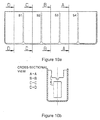
- both the hole connection described earlier and the strip connection also described earlier are used.
- the separating metal walls S1, S2, S3, S4 of the casing have all preferably same sized connection holes 5 through which an electromagnetical coupling is achieved between the resonators, which is mainly a capacitive coupling.
- the size of the coupling hole is either selected to preferably produce the main part of the coupling and the rest of the coupling is produced by the coupling arrangement in accordance with the invention, in which with a conductor, preferably a microstrip line provided near the resonator coil the additional capacitive coupling required is accomplished.
Landscapes
- Physics & Mathematics (AREA)
- Electromagnetism (AREA)
- Control Of Motors That Do Not Use Commutators (AREA)
- Filters And Equalizers (AREA)
Description
- The invention relates to a radio frequency filter which comprises at least two helix resonators disposed at a distance from each other, each of which is formed by a metal wire wound into a cylindrical coil.
- A filter comprising helix resonators is used widely in radio devices because of its good electrical properties and light structure. The resonator is a transmission line resonator and it is formed by a wire with a length of about a quarter of a wavelength wound into a cylindrical coil, which is placed in a grounded metal case. The characteristic impedance and accordingly the resonance frequency of the resonator are determined by physical dimensions of the cavity, by the ratio of the diameter of the helix coil to the inner dimension of the surrounding casing, and the distance between adjacent turns in the coil, i.e. the so called pitch, and the supporting structure possibly used for supporting the coil. Therefore producing a resonator with exactly a desired resonance frequency requires an accurate and uniform structure.
- A filter with desired properties can be built by cascading resonators and by arranging the coupling between them properly. When the filters get smaller especially in portable radio devices the accuracy requirements in production and assembly grow considerably, because even small variations in the dimensions of the cavity, the cylindrical coil and the supporting structure have great influence on the resonance frequency. When the filter is connected to an electrical circuit of a radio device its input and output ports must be matched with the circuit, i.e. the impedances from the ports to the filter must be the same as the impedances from the ports to the circuit to prevent reflections and transmission losses caused by sudden impedance changes. Also, the resonators of the filters must be matched with each other if the signal is brought to the filter by physical connection to its helix coil.
- A suitable impedance level has to be found in the helix resonator, that is, a physical point of connection at which the impedance level of the resonator equals that of a device connected thereto or an adjacent resonator. The impedance level of the connection point is directly proportional to the electrical length between the point of connection and the short-circuited end of the resonator, whereby a lower or higher impedance level can be selected by moving the point of connection along the helix coil. This kind of matching is called tapping because the point of connection forms a tap point from the helix resonator. The tap connection point in the helix resonator can be determined by experimentation or by calculation using a calculated or measured characteristic impedance of the helix resonator, which is determined by the properties of the resonator. In many cases, the tap point in the helix resonator is made in its first turn.
- Traditionally, tapping has been made by soldering one end of a discrete coil or conductor to the wire forming the helix resonator at the tap point. With decreasing filter sizes, the reproduction fidelity of such a tapping method has been found to be inadequate for series production. Inadequate accuracy in tapping results in a need for adjusting the tappings when tuning the filters, which increases tuning time and costs.
- A better tapping method has been presented in the Finnish patent 80542. The principle is shown in Figure 1. A
helix resonator 106 has been placed around aprojection 103 of a finger-likeinsulating plate 101 so that the projection is positioned inside the resonator coil, and thus supporting the coil. The end portion of the first turn of thecoil 106 close to theinsulating plate 101 is bent to form astraight portion 102 which is positioned tightly against the surface of the insulating plate over its entire length. This straight portion is called the leg of the resonator. Theend 107 of thestraight portion 102 is connected to thecasing 105 and is short-circuited through it. A micro-strip 108 is provided on the circuit board at the foot of theprojection 103 and is connected to the rest of the resonator circuit or forms a part of a more extensive microstrip pattern provided on the insulating plate. The direction of the microstrip is the same as the axis of the coil. The tapping point is thus the place where themicrostrip 108 crosses thestraight portion 102 of the coil. The strip and the straight portion are soldered together at this point. The tapping point and thus the desired impedance level are determined by moving the place of themicrostrip 108 sideways. - This method has the disadvantage of requiring several insulating plates which differ by the sideways position of the microstrip. This is a factor raising the expenses. Another disadvantage is that the tapping point cannot be fine tuned, because the leg must lie over the insulating plate. In practice, a leg lying over an insulating plate is not a very good solution, because a leg lying over an insulating plate with high losses increases the losses of the resonator.
- A filter which has been tapped to a microstrip on the edge of a finger-like projection as described above is well known from prior art. This kind of filter is shown in Figures 2, 3 and 4, in which reference numbers the same as in Figure 1 have been used when applicable. Figure 2 shows a part of a filter, which is surrounded by a casing, with four discrete helix resonator circuits - the
resonators like projections 103 of a printedboard 101. This is called a comb structure. An electrical circuit formed bystrip lines 108 and 108' runs at thebottom 101A of theinsulating plate 101, to which circuit one or several resonators, likeresonator 106, have been electrically connected by soldering at thetap point 121. Here the tap point is in the first turn of the coil but it can as well be placed higher. This possibility is shown in Figure 102 byresonator 107 in which thetap point 122 is in the second turn of the coil. In this case the microstrip protrudes little upwards on the finger-like projection and ends at the edge of it, whereto the turn of the resonator coil at that position is soldered. The tap point can thus be placed in any turn of the resonator coil and also several tap points can exist. Thestraight portion 102 of the resonator, unlike the leg in Figure 1, is bent in parallel with the axis of the resonator and runs at a distance from the insulating plate and its other end is connected during the assembly phase to thebottom plate 31 of the casing. Figure 3, and is grounded there through it if the plate is made of metal. The printed board of the radio device can also act as the bottom plate, at least one surface of which is coated with metal at the position of the filter, in which case the tip of the leg is connected to the metal coated surface. - Figure 4 shows an assembled filter according to the state of the art in which the filter casing is cut open to show the resonator more clearly. This filter has walls between the resonator circuits, the
walls 42 and 43 of which are shown, and these walls can have coupling holes (not shown in the figure) through which the circuit can be coupled electromagnetically to an adjacent circuit. The separating wall and the way the insulating plate, which supports the resonators, is connected to the walls of the casing are not essential to the present invention. Thecasing 41 is usually extruded aluminum and thebottom plate 44 can be a metal plate or a printed board with one metal coated surface. Thetap points helix resonators 106, which are shown, are marked with a black dot, and from this tap point the resonator is electrically connected to the microstrip circuit (not seen in Figure) provided on thebottom part 101A of the insulating plate and on thefingers 103. Thetips legs 102 and 102' are soldered to thebottom plate 44, if it or its coating is metal, or they are galvanically connected to the metal coating on the other side of the bottom plate, if the bottom plate is a printed board. - In radio frequency filters, which have at least two resonators, traditional fixed capacitors, which are suitable for relatively low frequency filters, can be used for providing the necessary coupling between the filter resonators. As the frequency increases the values of the coupling capacitors become so low that traditional capacitors cannot be used, but instead, for instance a board capacitance implemented on the printed board must be utilized, in which the necessary capacitance is formed by metal foil coupling electrodes on each side of the insulating material. In Helix filters described above and which have also been described e.g. in the US
patents 4 977 383 and 5 047 739 the couplings between the resonators are accomplished usually so that the separating metal wall has a hole of a certain size through which the resonators are coupled electromagnetically to each other. This has also been disclosed in the USpatent 5 157 363. When the hole is at the level of the open end of the resonators the coupling can be regarded mainly as capacitive and the holes can for simplicity be regarded as capacitors. The larger the hole of the separating wall is the higher is the capacitive coupling between the circuits. The amount of this coupling can be adjusted by altering the size of the hole in the separating metal wall. In this case, coupling holes of different sizes are often required in the same filter, whereby the tools required for making these holes together with the temporary tools required during the product development can raise the expenses considerably. - Changes of the mechanical position of the resonators in relation to the coupling hole alter the coupling between the circuits, which can be seen as deviations of the electrical properties of the filter. In addition, the inaccuracy in the production of the parts cause spreading in the couplings between the filter circuits.
- Figure 5 shows a circuit diagram of a typical band-pass filter consisting of two resonators, e.g. helix resonators. Usually the resonators are coupled so, that a coupling hole has been made in the separating metal wall between the resonators through which the resonance circuits are coupled. The capacitor C represents the capacitive coupling between the filter circuits. HX1 and HX2 represent transmission line resonators, preferably helix resonators and L1 and L2 represent coupling inductances by which resonators are coupled to the input and output ports, which usually have an impedance of 50 ohms. The length, the height in the cavity, the tap point etc. of the resonators must often be changed during the product development phase which means that the size of the coupling hole must be changed because of each change. This causes extra expenses to the product development and delays it.
- The construction in accordance with the invention has the advantage that it can lessen or even completely remove the problems described in the introduction and considerable cost savings can be achieved. In accordance with the invention, this is suitably accomplished by means of a conductor between two neighboring helix resonators, which is coupled to both resonators electromagnetically. In this way the resonators are coupled with each other through this conductor. WO-A-82 03499 discloses a radio frequency filter comprising two discrete helix resonators in which a conductor running between the resonators is provided such that one part of it is connected electromagnetically to one resonator and the other part of it is electromagnetically connected to the other resonator. According to the invention the conductor is made to go inside both resonator coils near the edge of the coil so that the required electromagnetic coupling is achieved In addition, the conductor is preferably a microstrip line, which has been arranged to run into both neighboring resonator coils on the insulating plate of a finger-like comb structured helix filter. Preferably the microstrip line is coupled to the resonator through a connection pad which is connected to the open end of the resonator coil or near to it, in which case the microstrip line is arranged near this pad so that it is mainly capacitively coupled to the pad.
- By using the coupling arrangement in accordance with the invention in helix resonators, especially during the development phase of the filters, making the required changes becomes easier and the development time of the product can be considerably reduced. Especially in very wide band filters e.g. in PCN filters, in which the width of the band is 75 MHz, the coupling between the circuits cannot even be accomplished properly with a traditional hole coupling.
- For coupling the neighboring resonators to each other the arrangement in accordance with the invention can be used alone and the filter can have a casing with no holes in the separating walls. Alternatively both the construction in accordance with the invention and the coupling holes in the separating walls may be used for coupling between the resonators. When the coupling construction in accordance with the invention is used, the hole in each separating wall of the casing of the helix filter can have the same size. In addition, the size of the connection hole can be selected so that the coupling is preferably mainly done through the hole and the remaining part of it is done by using the arrangement in accordance with the invention in which a conductor, preferably a microstrip line, arranged near the resonator coil can be used to make the required additional electromagnetic (capacitive) coupling. When the hole and conductor connection are used together the hole can have a standardized size and it is still possible to produce different kinds of filters, e.g. filters which differ from each other by bandwidth and frequency, by only changing the properties of the connection conductor according to the requirements. In this case only one tool instead of several ones is required for making the holes in the manufacturing of the filter. Different versions of filters are made easier and more quickly because only manufacturing a new conductor, e.g. a strip line on a printed board, is required for making changes in coupling, whereby also the development time of the product can be reduced considerably.
- The invention is described more thoroughly with the adjoining figures, in which:
- Figure 1
- shows a prior known tapping of a resonator,
- Figure 2
- shows the resonators of a prior known four circuit filter,
- Figure 3
- is a side view of one of the resonators in Figure 2,
- Figure 4
- shows a prior known filter partially opened,
- Figure 5
- shows the circuit diagram of a known band-pass filter comprising two resonators,
- Figure 6a
- shows a filter construction in accordance with the invention for coupling two helix resonators to each other,
- Figure 6b
- shows a filter .construction in accordance with the invention for coupling two helix resonators to each other,
- Figure 6c
- shows a filter construction in accordance with the invention for coupling two helix resonators to each other,
- Figure 7
- shows the circuit diagram of the construction in Figure 6,
- Figure 8a
- shows another filter construction in accordance with the invention,
- Figure 8b
- shows a construction in according to one embodiment seen from the opposite side than in Figure 8a,
- Figure 9
- shows the circuit diagram of the construction in Figure 8,
- Figure 10a
- shows a cross-sectional front view of the casing of a filter comprising helix resonators, and
- Figure 10b
- shows a sectional side view of Figure 10a.
- A description of Figures 1-5 was given earlier in connection with the description of the state of the art.
- A resonator structure in accordance with the invention is shown in Figure 6a, which shows a filter made of two helix resonators HX1, HX2. The helix resonators are made of a metal wire wound into a cylindrical coil and encircle a projection of an insulating plate, although the turns are shown cut so that the structure in accordance with invention is exposed more clearly. The helix resonators HX1 and HX2 are connected from their open ends to the connection points or
connection pads board 14 and from their tap points to thetapping pads part parts parts connection pads parts connection pad 1. Near the open end (top) of the resonator the coupling between connection strip and the resonator is mainly capacitive, but also inductive coupling can exist. Part of the electromagnetic coupling is produced by the coupling between the helix resonators HX1, HX2 and theparts connection pads connection pads branches - If it is desired to reduce the coupling between resonators, the length of the
branches connection point 12 of the first helix resonator HX1 and respectively at the output of the filter the strip line MLIN3 is provided between (theconnection point 13 of) the last resonator HX2 and the OUTPUT port of the filter. These strip lines MLIN1, MLIN3 function as transmission lines/inductances. - Figure 7 shows a circuit diagram of the structure according to Figure 6. The capacitors C1 and C2 are formed in the manner described above between the
connection point 1 and thepart connection point 2.Reference numbers parts parts 15 and 18 of the connection strips MLIN4 and MLIN6 end before the top of the helix resonators HX3, HX4. - Figure 8a illustrates a band-pass filter comprising four resonators. The helix resonators are designated by references HX1 - HX4, the connection strips in accordance with the invention are designated by references MLIN5-MLIN6, the INPUT and OUTPUT connection strips are designated by references MLIN1 and MLIN3. The helix resonators are formed of metal wires wound into a cylindrical coil, i.e.encircle a projection of the insulating plate, even if the turns of the coils of the helix resonators are shown cut to expose the structure better. The circuit diagram of the filter illustrated in Figure 8a is shown in Figure 9, in which the capacitors C1 and C6 are coupling capacitors of the kind shown in Figure 6. The capacitive connection to the resonators HX3, HX4 in the middle, between the end resonators HX1, HX2, is also accomplished using strip lines, but these are not connected to the connection pads but directly to the resonator coil. The capacitance C2 is formed by the capacitive connection between (the branch 15 of) the strip line MLIN4 and the resonator HX3. The capacitance C3 again is formed by the capacitive connection between (the
branch 16 of) the strip line MLIN5 and resonator HX3. Correspondingly the capacitance C4 is formed by the capacitive connection between (thebranch 17 of) the strip line MLIN5 and the resonator HX4 and correspondingly the capacitance C5 is formed by the capacitive connection between (thebranch 18 of) the strip line MLIN6 and the resonator HX4. The strip lines, which run near the resonators, in this case inside the resonator coils, form the coupling capacitances C2, C3, C4, C5 when the strip lines are coupled to the resonators. As well these strip lines could run outside the resonators, however, in the vicinity of the resonators. If the capacitive coupling between the resonators HX3 and HX4 is required to be reduced, the strip lines MLIN4 and/or MLIN5 can be shortened. The width of the strip line can be made narrower or the strip line can be moved sideways to adjust the distance d3 of the strip line from the resonator. - The coupling between resonators can also be arranged so that microstrip lines run on the opposite side to
connection pads board 14. In this case, the additional connections required, e.g. for producing the zero points required for the response, can be made on the spare space of the other side. The connection strips MLIN4, MLIN5, MLIN6 can be laid on the opposite side to the other coupling strips. This is shown in Figure 8b. In this case, connection strips MLIN4, MLIN5, MLIN6 do not run on the front side of the insulating plate. - In one embodiment in accordance with the invention this problem is lessened. In this embodiment both the hole connection described earlier and the strip connection also described earlier are used. In Figures 10a and 10b which show a casing of a band-pass filter, the separating metal walls S1, S2, S3, S4 of the casing have all preferably same sized connection holes 5 through which an electromagnetical coupling is achieved between the resonators, which is mainly a capacitive coupling. The size of the coupling hole is either selected to preferably produce the main part of the coupling and the rest of the coupling is produced by the coupling arrangement in accordance with the invention, in which with a conductor, preferably a microstrip line provided near the resonator coil the additional capacitive coupling required is accomplished. By using hole and conductor (mictrostrip line) couplings together, different filters with only one standard connection hole can be produced, e.g. such filters, which differ from each other by the bandwidth or frequency, can be produced only by changing the properties of the connection conductor (microstrip line) in accordance with the invention to respond each situation. Only one tool is required for manufacturing the filter for forming the connection holes instead of several tools required earlier. Filter versions with different properties are produced more easily and faster because the coupling can be changed by making only a new strip line pattern on a printed board, whereby also the development of the product is faster.
Claims (6)
- A radio frequency filter comprising at least first and second discrete helix resonators placed at a distance from each other, a conductor having electromagnetic coupling to first and second resonators, and an insulating plate having projections, each of said resonators being wound of metal wire around one of said projections, characterized in that said conductor is a strip line (MLIN2, MLIN4-MLIN6) on the surface of said insulating plate (14) so that one part (3, 16) of the strip line is lying on one projection inside the first resonator coil (HX1, HX3) and another part (4, 17) on another projection inside the other resonator coil (HX2, HX4).
- A radio frequency filter according to claim 1, characterized in that a connection pad (1, 2, 19, 20) is provided on the insulating plate (14) and is in contact with the resonator coil at or near the open end of the coil (HX1 - HX4) and one of the parts (3 - 8, 15 - 18) of the strip line (MLIN2, MLIN4-MLIN6) is provided near said connection pad (1, 2, 19, 20) and is electromagnetically coupled to the resonator through the connection pad.
- A radio frequency filter according to claim 1, characterized in that the conductor is mainly capacitively coupled to the resonator.
- A radio frequency filter according to claim 2, characterized in that it comprises more than two resonators and microstrip lines have been provided on both sides of the insulating plate (14).
- A radio frequency filter according to claim 4, characterized in that said connection pad (1, 2, 19, 20) which is in contact with the resonator coil is on one side of the insulating plate (14) and on the other side of the insulating plate there is provided the second strip line (MLIN5, MLIN6) connecting two neighboring resonators and it is provided at the position of the connection pad (1, 2, 19, 20) being electromagnetically coupled to the connection pad through the insulating plate.
- A radio frequency filter according to one of the previous claims, characterized in that the filter further comprises of a metal or metal clad casing in which the helix resonators (HX1 - HX4) have been separated from each other by a separating metal or metal clad wall, which has a hole (5) through which neighboring resonators are connected electromagnetically to each other.
Applications Claiming Priority (2)
| Application Number | Priority Date | Filing Date | Title |
|---|---|---|---|
| FI944701A FI96998C (en) | 1994-10-07 | 1994-10-07 | Radio frequency filter with Helix resonators |
| FI944701 | 1994-10-07 |
Publications (2)
| Publication Number | Publication Date |
|---|---|
| EP0706230A1 EP0706230A1 (en) | 1996-04-10 |
| EP0706230B1 true EP0706230B1 (en) | 2001-08-01 |
Family
ID=8541535
Family Applications (1)
| Application Number | Title | Priority Date | Filing Date |
|---|---|---|---|
| EP95307092A Expired - Lifetime EP0706230B1 (en) | 1994-10-07 | 1995-10-06 | Radio frequency filter comprising helix resonators |
Country Status (7)
| Country | Link |
|---|---|
| US (1) | US5689221A (en) |
| EP (1) | EP0706230B1 (en) |
| JP (1) | JPH08181505A (en) |
| AU (1) | AU701521B2 (en) |
| CA (1) | CA2158378A1 (en) |
| DE (1) | DE69521956T2 (en) |
| FI (1) | FI96998C (en) |
Families Citing this family (41)
| Publication number | Priority date | Publication date | Assignee | Title |
|---|---|---|---|---|
| EP0828306A3 (en) * | 1996-09-03 | 2000-03-22 | Lk-Products Oy | A matched impedance filter |
| GB0006409D0 (en) * | 2000-03-16 | 2000-05-03 | Cryosystems | Electrical filter |
| FI115331B (en) * | 2000-09-22 | 2005-04-15 | Filtronic Comtek Oy | High Pass Filter |
| DE10123369A1 (en) * | 2001-05-14 | 2002-12-05 | Infineon Technologies Ag | Filter arrangement for, symmetrical and asymmetrical pipe systems |
| WO2006000650A1 (en) | 2004-06-28 | 2006-01-05 | Pulse Finland Oy | Antenna component |
| FI20055420A0 (en) | 2005-07-25 | 2005-07-25 | Lk Products Oy | Adjustable multi-band antenna |
| FI119009B (en) | 2005-10-03 | 2008-06-13 | Pulse Finland Oy | Multiple-band antenna |
| FI118782B (en) | 2005-10-14 | 2008-03-14 | Pulse Finland Oy | Adjustable antenna |
| FI119577B (en) * | 2005-11-24 | 2008-12-31 | Pulse Finland Oy | The multiband antenna component |
| US8618990B2 (en) | 2011-04-13 | 2013-12-31 | Pulse Finland Oy | Wideband antenna and methods |
| US10211538B2 (en) | 2006-12-28 | 2019-02-19 | Pulse Finland Oy | Directional antenna apparatus and methods |
| FI20075269A0 (en) | 2007-04-19 | 2007-04-19 | Pulse Finland Oy | Method and arrangement for antenna matching |
| FI120427B (en) | 2007-08-30 | 2009-10-15 | Pulse Finland Oy | Adjustable multiband antenna |
| FI20096134A0 (en) | 2009-11-03 | 2009-11-03 | Pulse Finland Oy | Adjustable antenna |
| FI20096251A0 (en) | 2009-11-27 | 2009-11-27 | Pulse Finland Oy | MIMO antenna |
| US8847833B2 (en) | 2009-12-29 | 2014-09-30 | Pulse Finland Oy | Loop resonator apparatus and methods for enhanced field control |
| FI20105158A7 (en) | 2010-02-18 | 2011-08-19 | Pulse Finland Oy | ANTENNA EQUIPPED WITH SHELL RADIATOR |
| US9406998B2 (en) | 2010-04-21 | 2016-08-02 | Pulse Finland Oy | Distributed multiband antenna and methods |
| FI20115072A0 (en) | 2011-01-25 | 2011-01-25 | Pulse Finland Oy | Multi-resonance antenna, antenna module and radio unit |
| US9673507B2 (en) | 2011-02-11 | 2017-06-06 | Pulse Finland Oy | Chassis-excited antenna apparatus and methods |
| US8648752B2 (en) | 2011-02-11 | 2014-02-11 | Pulse Finland Oy | Chassis-excited antenna apparatus and methods |
| US8866689B2 (en) | 2011-07-07 | 2014-10-21 | Pulse Finland Oy | Multi-band antenna and methods for long term evolution wireless system |
| US9450291B2 (en) | 2011-07-25 | 2016-09-20 | Pulse Finland Oy | Multiband slot loop antenna apparatus and methods |
| US9123990B2 (en) | 2011-10-07 | 2015-09-01 | Pulse Finland Oy | Multi-feed antenna apparatus and methods |
| US9531058B2 (en) | 2011-12-20 | 2016-12-27 | Pulse Finland Oy | Loosely-coupled radio antenna apparatus and methods |
| US9484619B2 (en) | 2011-12-21 | 2016-11-01 | Pulse Finland Oy | Switchable diversity antenna apparatus and methods |
| US8988296B2 (en) | 2012-04-04 | 2015-03-24 | Pulse Finland Oy | Compact polarized antenna and methods |
| US9979078B2 (en) | 2012-10-25 | 2018-05-22 | Pulse Finland Oy | Modular cell antenna apparatus and methods |
| US10069209B2 (en) | 2012-11-06 | 2018-09-04 | Pulse Finland Oy | Capacitively coupled antenna apparatus and methods |
| KR102028057B1 (en) * | 2013-01-22 | 2019-10-04 | 삼성전자주식회사 | Resonator with improved isolation |
| US10079428B2 (en) | 2013-03-11 | 2018-09-18 | Pulse Finland Oy | Coupled antenna structure and methods |
| US9647338B2 (en) | 2013-03-11 | 2017-05-09 | Pulse Finland Oy | Coupled antenna structure and methods |
| US9634383B2 (en) | 2013-06-26 | 2017-04-25 | Pulse Finland Oy | Galvanically separated non-interacting antenna sector apparatus and methods |
| US9680212B2 (en) | 2013-11-20 | 2017-06-13 | Pulse Finland Oy | Capacitive grounding methods and apparatus for mobile devices |
| US9590308B2 (en) | 2013-12-03 | 2017-03-07 | Pulse Electronics, Inc. | Reduced surface area antenna apparatus and mobile communications devices incorporating the same |
| US9350081B2 (en) | 2014-01-14 | 2016-05-24 | Pulse Finland Oy | Switchable multi-radiator high band antenna apparatus |
| US9973228B2 (en) | 2014-08-26 | 2018-05-15 | Pulse Finland Oy | Antenna apparatus with an integrated proximity sensor and methods |
| US9948002B2 (en) | 2014-08-26 | 2018-04-17 | Pulse Finland Oy | Antenna apparatus with an integrated proximity sensor and methods |
| US9722308B2 (en) | 2014-08-28 | 2017-08-01 | Pulse Finland Oy | Low passive intermodulation distributed antenna system for multiple-input multiple-output systems and methods of use |
| US9906260B2 (en) | 2015-07-30 | 2018-02-27 | Pulse Finland Oy | Sensor-based closed loop antenna swapping apparatus and methods |
| CN115663430B (en) * | 2022-12-28 | 2023-03-21 | 成都世源频控技术股份有限公司 | Spiral winding shaft type microstrip filter and preparation method thereof |
Family Cites Families (13)
| Publication number | Priority date | Publication date | Assignee | Title |
|---|---|---|---|---|
| US3621484A (en) * | 1970-03-05 | 1971-11-16 | Motorola Inc | Helical resonator having variable capacitor which includes windings of reduced diameter as one plate thereof |
| GB1602770A (en) * | 1977-06-03 | 1981-11-18 | Matsushita Electric Industrial Co Ltd | Band pass filter |
| US4374370A (en) * | 1981-03-30 | 1983-02-15 | Motorola, Inc. | Helical resonator filter |
| US4740765A (en) * | 1985-09-30 | 1988-04-26 | Murata Manufacturing Co., Ltd. | Dielectric filter |
| US4816788A (en) * | 1986-07-01 | 1989-03-28 | Murata Manufacturing Co., Ltd. | High frequency band-pass filter |
| US4800347A (en) * | 1986-09-04 | 1989-01-24 | Murata Manufacturing Co., Ltd. | Dielectric filter |
| JPH0713284Y2 (en) * | 1987-09-21 | 1995-03-29 | 株式会社村田製作所 | Resonant frequency adjustment structure for integrally molded dielectric filter |
| JPH01112801A (en) * | 1987-10-26 | 1989-05-01 | Kokusai Electric Co Ltd | dielectric bandpass filter |
| FI78198C (en) * | 1987-11-20 | 1989-06-12 | Lk Products Oy | Överföringsledningsresonator |
| FI80542C (en) | 1988-10-27 | 1990-06-11 | Lk Products Oy | resonator |
| FI87405C (en) | 1990-02-07 | 1992-12-28 | Lk Products Oy | HOEGFREKVENSFILTER |
| US5432489A (en) * | 1992-03-09 | 1995-07-11 | Lk-Products Oy | Filter with strip lines |
| FI91116C (en) * | 1992-04-21 | 1994-05-10 | Lk Products Oy | Helix resonator |
-
1994
- 1994-10-07 FI FI944701A patent/FI96998C/en not_active IP Right Cessation
-
1995
- 1995-09-15 CA CA002158378A patent/CA2158378A1/en not_active Abandoned
- 1995-10-02 AU AU32988/95A patent/AU701521B2/en not_active Ceased
- 1995-10-06 EP EP95307092A patent/EP0706230B1/en not_active Expired - Lifetime
- 1995-10-06 DE DE69521956T patent/DE69521956T2/en not_active Expired - Fee Related
- 1995-10-06 US US08/539,820 patent/US5689221A/en not_active Expired - Fee Related
- 1995-10-06 JP JP7260372A patent/JPH08181505A/en active Pending
Also Published As
| Publication number | Publication date |
|---|---|
| US5689221A (en) | 1997-11-18 |
| DE69521956D1 (en) | 2001-09-06 |
| EP0706230A1 (en) | 1996-04-10 |
| DE69521956T2 (en) | 2002-04-04 |
| FI96998B (en) | 1996-06-14 |
| FI944701L (en) | 1996-04-08 |
| AU3298895A (en) | 1996-04-18 |
| JPH08181505A (en) | 1996-07-12 |
| FI96998C (en) | 1996-09-25 |
| AU701521B2 (en) | 1999-01-28 |
| FI944701A0 (en) | 1994-10-07 |
| CA2158378A1 (en) | 1996-04-08 |
Similar Documents
| Publication | Publication Date | Title |
|---|---|---|
| US5689221A (en) | Radio frequency filter comprising helix resonators | |
| US4977383A (en) | Resonator structure | |
| US5585771A (en) | Helical resonator filter including short circuit stub tuning | |
| US5675301A (en) | Dielectric filter having resonators aligned to effect zeros of the frequency response | |
| US5739735A (en) | Filter with improved stop/pass ratio | |
| US5047739A (en) | Transmission line resonator | |
| US5351023A (en) | Helix resonator | |
| US5731749A (en) | Transmission line resonator filter with variable slot coupling and link coupling #10 | |
| GB2269715A (en) | RF filters | |
| KR100401967B1 (en) | High frequency filter, filter device, and electronic apparatus incorporating the same | |
| US5136269A (en) | High-frequency band-pass filter having multiple resonators for providing high pass-band attenuation | |
| JP3921370B2 (en) | High frequency filter | |
| KR19980063241A (en) | Dielectric filter | |
| US6924718B2 (en) | Coupling probe having an adjustable tuning conductor | |
| US5563561A (en) | Dielectric block apparatus having two opposing coaxial resonators separated by an electrode free region | |
| KR20010021163A (en) | Dielectric Duplexer and Communication Apparatus | |
| JPS6314501A (en) | high frequency filter | |
| FI87406B (en) | BAND PASS FILTER. | |
| EP0797267A2 (en) | Radio frequency filter and a method for adjusting the frequency response thereof | |
| EP0369757A2 (en) | Helical filter | |
| FI87407C (en) | Bandpass Filter | |
| JPS62181504A (en) | Filter | |
| JPS63234701A (en) | high frequency filter |
Legal Events
| Date | Code | Title | Description |
|---|---|---|---|
| PUAI | Public reference made under article 153(3) epc to a published international application that has entered the european phase |
Free format text: ORIGINAL CODE: 0009012 |
|
| AK | Designated contracting states |
Kind code of ref document: A1 Designated state(s): CH DE DK FR GB IT LI SE |
|
| 17P | Request for examination filed |
Effective date: 19961010 |
|
| 17Q | First examination report despatched |
Effective date: 19990804 |
|
| RAP1 | Party data changed (applicant data changed or rights of an application transferred) |
Owner name: FILTRONIC LK OY |
|
| GRAG | Despatch of communication of intention to grant |
Free format text: ORIGINAL CODE: EPIDOS AGRA |
|
| GRAG | Despatch of communication of intention to grant |
Free format text: ORIGINAL CODE: EPIDOS AGRA |
|
| GRAH | Despatch of communication of intention to grant a patent |
Free format text: ORIGINAL CODE: EPIDOS IGRA |
|
| GRAH | Despatch of communication of intention to grant a patent |
Free format text: ORIGINAL CODE: EPIDOS IGRA |
|
| GRAA | (expected) grant |
Free format text: ORIGINAL CODE: 0009210 |
|
| AK | Designated contracting states |
Kind code of ref document: B1 Designated state(s): CH DE DK FR GB IT LI SE |
|
| PG25 | Lapsed in a contracting state [announced via postgrant information from national office to epo] |
Ref country code: LI Free format text: LAPSE BECAUSE OF FAILURE TO SUBMIT A TRANSLATION OF THE DESCRIPTION OR TO PAY THE FEE WITHIN THE PRESCRIBED TIME-LIMIT Effective date: 20010801 Ref country code: IT Free format text: LAPSE BECAUSE OF FAILURE TO SUBMIT A TRANSLATION OF THE DESCRIPTION OR TO PAY THE FEE WITHIN THE PRESCRIBED TIME-LIMIT;WARNING: LAPSES OF ITALIAN PATENTS WITH EFFECTIVE DATE BEFORE 2007 MAY HAVE OCCURRED AT ANY TIME BEFORE 2007. THE CORRECT EFFECTIVE DATE MAY BE DIFFERENT FROM THE ONE RECORDED. Effective date: 20010801 Ref country code: CH Free format text: LAPSE BECAUSE OF FAILURE TO SUBMIT A TRANSLATION OF THE DESCRIPTION OR TO PAY THE FEE WITHIN THE PRESCRIBED TIME-LIMIT Effective date: 20010801 |
|
| REG | Reference to a national code |
Ref country code: CH Ref legal event code: EP |
|
| REF | Corresponds to: |
Ref document number: 69521956 Country of ref document: DE Date of ref document: 20010906 |
|
| PG25 | Lapsed in a contracting state [announced via postgrant information from national office to epo] |
Ref country code: SE Free format text: LAPSE BECAUSE OF FAILURE TO SUBMIT A TRANSLATION OF THE DESCRIPTION OR TO PAY THE FEE WITHIN THE PRESCRIBED TIME-LIMIT Effective date: 20011101 Ref country code: DK Free format text: LAPSE BECAUSE OF FAILURE TO SUBMIT A TRANSLATION OF THE DESCRIPTION OR TO PAY THE FEE WITHIN THE PRESCRIBED TIME-LIMIT Effective date: 20011101 |
|
| EN | Fr: translation not filed | ||
| REG | Reference to a national code |
Ref country code: GB Ref legal event code: IF02 |
|
| REG | Reference to a national code |
Ref country code: CH Ref legal event code: PL |
|
| EN | Fr: translation not filed |
Free format text: BO 01/52 PAGES: 283, IL Y A LIEU DE SUPPRIMER: LA MENTION DE LA NON REMISE. LA REMISE EST PUBLIEE DANS LE PRESENT BOPI. |
|
| ET | Fr: translation filed | ||
| PLBE | No opposition filed within time limit |
Free format text: ORIGINAL CODE: 0009261 |
|
| STAA | Information on the status of an ep patent application or granted ep patent |
Free format text: STATUS: NO OPPOSITION FILED WITHIN TIME LIMIT |
|
| 26N | No opposition filed | ||
| PGFP | Annual fee paid to national office [announced via postgrant information from national office to epo] |
Ref country code: GB Payment date: 20031001 Year of fee payment: 9 |
|
| PGFP | Annual fee paid to national office [announced via postgrant information from national office to epo] |
Ref country code: FR Payment date: 20031003 Year of fee payment: 9 |
|
| PGFP | Annual fee paid to national office [announced via postgrant information from national office to epo] |
Ref country code: DE Payment date: 20031016 Year of fee payment: 9 |
|
| PG25 | Lapsed in a contracting state [announced via postgrant information from national office to epo] |
Ref country code: GB Free format text: LAPSE BECAUSE OF NON-PAYMENT OF DUE FEES Effective date: 20041006 |
|
| PG25 | Lapsed in a contracting state [announced via postgrant information from national office to epo] |
Ref country code: DE Free format text: LAPSE BECAUSE OF NON-PAYMENT OF DUE FEES Effective date: 20050503 |
|
| GBPC | Gb: european patent ceased through non-payment of renewal fee |
Effective date: 20041006 |
|
| PG25 | Lapsed in a contracting state [announced via postgrant information from national office to epo] |
Ref country code: FR Free format text: LAPSE BECAUSE OF NON-PAYMENT OF DUE FEES Effective date: 20050630 |
|
| REG | Reference to a national code |
Ref country code: FR Ref legal event code: ST |