EP0706027B1 - Visual inspection apparatus for printed circuit boards and use thereof for solder control and correction - Google Patents
Visual inspection apparatus for printed circuit boards and use thereof for solder control and correction Download PDFInfo
- Publication number
- EP0706027B1 EP0706027B1 EP94913789A EP94913789A EP0706027B1 EP 0706027 B1 EP0706027 B1 EP 0706027B1 EP 94913789 A EP94913789 A EP 94913789A EP 94913789 A EP94913789 A EP 94913789A EP 0706027 B1 EP0706027 B1 EP 0706027B1
- Authority
- EP
- European Patent Office
- Prior art keywords
- board
- visual inspection
- supporting apparatus
- image
- stage
- Prior art date
- Legal status (The legal status is an assumption and is not a legal conclusion. Google has not performed a legal analysis and makes no representation as to the accuracy of the status listed.)
- Expired - Lifetime
Links
Images


Classifications
-
- G—PHYSICS
- G01—MEASURING; TESTING
- G01B—MEASURING LENGTH, THICKNESS OR SIMILAR LINEAR DIMENSIONS; MEASURING ANGLES; MEASURING AREAS; MEASURING IRREGULARITIES OF SURFACES OR CONTOURS
- G01B11/00—Measuring arrangements characterised by the use of optical techniques
- G01B11/24—Measuring arrangements characterised by the use of optical techniques for measuring contours or curvatures
-
- G—PHYSICS
- G01—MEASURING; TESTING
- G01R—MEASURING ELECTRIC VARIABLES; MEASURING MAGNETIC VARIABLES
- G01R31/00—Arrangements for testing electric properties; Arrangements for locating electric faults; Arrangements for electrical testing characterised by what is being tested not provided for elsewhere
- G01R31/28—Testing of electronic circuits, e.g. by signal tracer
- G01R31/302—Contactless testing
- G01R31/308—Contactless testing using non-ionising electromagnetic radiation, e.g. optical radiation
- G01R31/309—Contactless testing using non-ionising electromagnetic radiation, e.g. optical radiation of printed or hybrid circuits or circuit substrates
-
- G—PHYSICS
- G01—MEASURING; TESTING
- G01R—MEASURING ELECTRIC VARIABLES; MEASURING MAGNETIC VARIABLES
- G01R31/00—Arrangements for testing electric properties; Arrangements for locating electric faults; Arrangements for electrical testing characterised by what is being tested not provided for elsewhere
- G01R31/28—Testing of electronic circuits, e.g. by signal tracer
- G01R31/2801—Testing of printed circuits, backplanes, motherboards, hybrid circuits or carriers for multichip packages [MCP]
- G01R31/281—Specific types of tests or tests for a specific type of fault, e.g. thermal mapping, shorts testing
-
- H—ELECTRICITY
- H05—ELECTRIC TECHNIQUES NOT OTHERWISE PROVIDED FOR
- H05K—PRINTED CIRCUITS; CASINGS OR CONSTRUCTIONAL DETAILS OF ELECTRIC APPARATUS; MANUFACTURE OF ASSEMBLAGES OF ELECTRICAL COMPONENTS
- H05K13/00—Apparatus or processes specially adapted for manufacturing or adjusting assemblages of electric components
- H05K13/08—Monitoring manufacture of assemblages
- H05K13/081—Integration of optical monitoring devices in assembly lines; Processes using optical monitoring devices specially adapted for controlling devices or machines in assembly lines
- H05K13/0815—Controlling of component placement on the substrate during or after manufacturing
-
- H—ELECTRICITY
- H01—ELECTRIC ELEMENTS
- H01L—SEMICONDUCTOR DEVICES NOT COVERED BY CLASS H10
- H01L22/00—Testing or measuring during manufacture or treatment; Reliability measurements, i.e. testing of parts without further processing to modify the parts as such; Structural arrangements therefor
- H01L22/10—Measuring as part of the manufacturing process
- H01L22/12—Measuring as part of the manufacturing process for structural parameters, e.g. thickness, line width, refractive index, temperature, warp, bond strength, defects, optical inspection, electrical measurement of structural dimensions, metallurgic measurement of diffusions
-
- H—ELECTRICITY
- H01—ELECTRIC ELEMENTS
- H01L—SEMICONDUCTOR DEVICES NOT COVERED BY CLASS H10
- H01L2924/00—Indexing scheme for arrangements or methods for connecting or disconnecting semiconductor or solid-state bodies as covered by H01L24/00
- H01L2924/0001—Technical content checked by a classifier
- H01L2924/0002—Not covered by any one of groups H01L24/00, H01L24/00 and H01L2224/00
Definitions
- the present invention relates to a visual inspection supporting apparatus which is used for an inspector to visually inspect acceptability of soldering of electronic parts mounted on a printed circuit board, and the use of said apparatus for correcting an unacceptable soldered portion during manufacture of a printed circuit board.
- a visual inspection supporting apparatus for example, a visual inspection supporting apparatus, a printed circuit board inspecting apparatus, an automatic printed circuit board inspecting apparatus, and an external appearance inspecting apparatus
- light sources of the three primary colors i.e., red (R), green (G) and blue (B) are generally used.
- the light sources are so arranged as to project illuminating light at different angles to a portion to be inspected.
- inclined surfaces or flat surfaces having different angles are indicated in different colors. Consequently, color information can be also utilized for judging whether or not soldering is acceptable.
- the visual inspection has the advantage that when an unacceptable soldered portion is found out, the unacceptable soldered portion can be immediately corrected. It has been desired to realize a suitable apparatus for supporting such visual inspection.
- EP 0 413 817 A1 discloses a substrate examining device for inspection of soldered parts on the substrate.
- the substrate is mounted on a y-movement table and an inspection camera including ring-shaped illuminating elements are installed on an X-movement table thereby providing an XY-movement of the camera relative to the substrate surface.
- a viewing assembly is mounted on a XY-movement device for scanning the viewing assembly parallel to a table supporting a PCB to be inspected.
- US 4,832,250 A discloses a semi-automated electronic circuit board rework and repair system, comprising a table movable along guide rods of a plate in y-direction, wherein the plate is movable on guide rods in x-direction.
- US 4,566,325 A discloses an inspection board for PCBs.
- a platen 50 is slidably supported on guide rods which are attached to support blocks.
- the support blocks are slidably attached to guide rails.
- Guide rails and supports form a frame which is pivotably attached to a base, e.g. the lower edge is hinged to the base. Further the base can be a light table with a light transmitting top.
- An object of the present invention is to provide a supporting apparatus for PCB visual inspection and correction of an unacceptable portion which makes it easy for an inspector to perform work and makes it possible to improve operation (work) efficiency.
- Another object of the present invention is to provide a visual inspection supporting apparatus capable of ensuring the objectivity of judgment by an inspector.
- the apparatus of the present invention can be developed into not only support of visual inspection but also automatic inspection.
- Using the visual inspection supporting apparatus according to the present invention allows to judge whether or not soldering on a printed circuit board is acceptable and to correct a soldered portion which is judged to be unacceptable.
- a visual inspection supporting apparatus comprises a illuminating device for illuminating a printed circuit board to be inspected, an imaging device for imaging an area on the board illuminated by the illuminating device and outputting an image signal representing an image obtained by the imaging, a stage which is movable relatively to the illuminating device and the imaging device in two perpendicular directions, a board supporting member supported on the stage for supporting the board to be inspected, and a mechanism for moving the stage until the board supported on the board supporting member reaches a position outside of a range in which the illuminating device and the imaging device exist.
- a display device for displaying the image represented by the image signal outputted from the imaging device.
- the visual inspection supporting apparatus is suitable for not only inspection but also correction of an unacceptable portion. Since the board supported on the stage is drawn out of the range in which the illuminating device and the imaging device exist, it is possible to correct the unacceptable portion at the position where the board is drawn out.
- the board supporting member is rotatably supported on the stage so as to be capable of being obliquely raised and laid down, and provided is a mechanism for holding the board supporting member in its obliquely raised position.
- the image obtained by the imaging before the stage is drawn out is frozen and is displayed as a still image on the display device.
- the inspector can search for the unacceptable portion on the board by seeing the image.
- the apparatus is suitable for soldering inspection and correction of a part having a lead on four perpendicular sides.
- the visual inspection supporting apparatus further comprises storage means for storing previously taught position data representing a point to be inspected on a board to be inspected and display control means for performing control so as to indicate the point to be inspected on the image displayed on the display device in accordance with the position data stored in the storage means.
- the result of the inspection is immediately entered from an input device.
- a portion which is judged to be unacceptable as the result of the inspection is indicated on a screen of the display device.
- a layout display indicating the position on the board of an area of the image displayed on the display device is provided. Consequently, the inspector can find an area currently inspected, and can also grasp the progress of the inspection.
- a scale for expressing the length is displayed on the image displayed on the display device.
- two lines are movably displayed on the display screen of the display device, and the spacing between the two lines is calculated and is displayed.
- a window is displayed on the display screen of the display device, and data relating to the size of a particular image in the window is displayed. More preferably, data relating to the reference size is displayed in addition to the data relating to the size of the particular image.
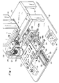
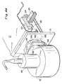
- FIG. 1 to 4 An example of the mechanical construction of a visual inspection supporting apparatus for assisting in work for visually inspecting a printed circuit (PC) board on which parts are mounted for acceptability of soldering is illustrated in Figs. 1 to 4 .
- PC printed circuit
- a printed circuit board on which electronic parts are mounted is generally manufactured through a mounting step for disposing and positioning an electronic part (hereinafter merely referred to as a "part") on a printed circuit board (hereinafter merely referred to as a "PC board” or “board”), a soldering step using soldering methods such as a flow soldering method and a reflow soldering method, a soldering inspecting step for judging whether or not soldering is acceptable, and a soldering correcting step for correcting a soldered portion which is judged to be unacceptable.
- No soldering correcting step is, of course, required with respect to a PC board having no unacceptable soldered portion.
- the soldering step and the subsequent steps may, in some cases, be performed again with respect to a PC board having a soldered portion difficult or impossible to correct.
- the visual inspection supporting apparatus is used for either one or both of the soldering inspecting step and the soldering correcting step. That is, the visual inspection supporting apparatus is used for assisting an inspector (a worker) in performing work for visually inspecting a soldered portion on a PC board for acceptability and assisting a worker (an inspector) in performing manual work for correcting an unacceptable soldered portion.
- an unacceptable portion can be corrected after visual inspection of one or a plurality of PC boards is completed, and an unacceptable portion can be also corrected every time the unacceptable portion is found out in visual inspection of one PC board.
- a fixed table 11 is positioned on the rear half of a base 10, and legs 12 of the table 11 are secured to the base 10.
- the upper surface of the table 11 is higher in position than the base 10, and a CRT display device 13 is disposed on the upper surface of the table 11.
- An X-axis table 20 is provided along the front edge of the table 11.
- a Y-axis table 30 is provided on the base 10 in such an arrangement as to perpendicularly cross the X-axis table 20.
- the X-axis table 20 moves in the X-axis direction and positions a light projecting device 70 and an imaging device 80.
- the Y-axis table 30 moves in the Y-axis direction and positions a PC board PCB.
- the X-axis table 20 is mounted on the lower surface of the front edge of the table 11, and comprises an X-axis rail 23 and a supporting rail 24 extending in the transverse direction (the X-axis direction).
- An X stage 21 is provided with a slider 22.
- the slider 22 is slidably fitted to the X-axis rail 23.
- a portion including the slider 22 of the X stage 21 is slidably supported on the supporting rail 24.
- An endless timing belt 25 is disposed along the X-axis rail 23.
- the timing belt 25 is reeved around pulleys (gears) 27 and 28 each having teeth on its peripheral surface.
- the pulley 27 is rotatably mounted on the lower surface of the table 11 at one end thereof, and the pulley 28 is fixed to the rotational shaft of an X-axis motor (a DC motor) 29.
- the motor 29 is fixed to the lower surface of the table 11.
- the timing belt 25 is attached to the X stage 21 at its one portion.
- the X stage 21 is moved rightward and leftward along the X-axis rail 23 via the timing belt 25 and is placed in an arbitrary position.
- the light projecting device 70 and the imaging device 80 are mounted on the X stage 21.
- the Y-axis table 30 comprises a Y-axis rail 33 secured to the base 10.
- the Y-axis rail 33 perpendicularly crosses the X-axis rail 23.
- a Y stage 41 comprises a supporting plate 43, a sliding member 42 fixed to the lower surface of the supporting plate 43, side members 44 formed integrally with the supporting plate 43 on both sides thereof and extending in the longitudinal direction (the Y-axis direction), and a rear member 45 fixed between the rear ends of the side members 44.
- the sliding member 42 is slidably fitted to the Y-axis rail 33.
- An endless timing belt 35 is disposed along the Y-axis rail 33.
- Pulleys (gears) 37 and 38 each having teeth formed on its peripheral surface are rotatably provided at the front end and the rear end of the base 10, respectively.
- the timing belt 35 is reeved around the pulleys 37 and 38.
- a portion of the timing belt 35 is attached to a bracket 43a fixed to the lower surface of the supporting plate 43.
- a pulley 31 and the pulley 38 at the rear of the base 10 are secured to a common shaft.
- a pulley 36 is fixed to the rotational shaft of a Y-axis motor (a DC motor) 39.
- a timing belt 32 is reeved around the pulleys 31 and 36.
- the common rotational shaft of the pulleys 31 and 38 is rotatably supported by a suitable bearing (not shown).
- the bearing and the motor 39 are fixed to the base 10 by a fixing member (not shown).
- a frame 34 is provided around the Y-axis rail 33 and the timing belt 35.
- the frame 34 is fixed to the base 10.
- a stopper 34a and a stopper 34b are respectively fixed to the front end and the rear end of the frame 34.
- the stoppers 34a and 34b regulate the movement range of the Y stage 41.
- a cover (not shown) is attached to the frame 34 in such a manner as not to prevent the movement of the Y stage 41.
- the Y stage 41 By driving the Y-axis motor 39, the Y stage 41 is moved back and forth along the rail 33 via the timing belts 32 and 35 and is placed in an arbitrary position.
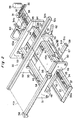
- a board supporting body 50 is mounted on the Y stage 41 so as to be capable of being raised and laid down.
- the board supporting body 50 comprises a front plate 51, a movable plate 52, a rear plate 53, and rods 54.
- Each of the front plate 51 and the movable plate 52 has leg portions extending downward from both ends thereof.
- Supporting arms 51A and 52A horizontally extending in the transverse direction (the rightward/leftward direction) are integrally formed in the upper portions of the front plate 51 and the movable plate 52, respectively.
- the rear plate 53 has leg portions extending downward from both ends thereof.
- the leg portions of the front plate 51 and the leg portions of the rear plate 53 are respectively connected by the rods 54. Both ends of the rod 54 are respectively fixed to the leg portions of the front plate 51 and the rear plate 53.
- Cylinders 55 are perpendicularly fixed to the leg portions of the movable plate 52, respectively.
- the leg portions of the movable plate 52 are respectively provided with holes corresponding to through holes of the cylinders 55.
- the rods 54 slidably pass through the through holes of the cylinders 55 and the holes of the leg portions, respectively. Consequently, the movable plate 52 is movable along the rods 54 between the front and rear plates 51 and 53.
- a splitted piece 61 is fixedly attached to one of the leg portions of the movable plate 52, on a surface opposite to the surface where the cylinder 55 is mounted, of the movable plate 52.
- the splitted piece 61 also has a hole through which the rod 54 slidably passes, and a slit 61a is formed downward from the hole.
- a screw hole is formed in a direction perpendicular to the slit 61a, and a screw 62a integrally secured to a lever 62 is fitted in the screw hole.
- the screw 62a is screwed in the screw hole by means of the lever 62, whereby the hole of the splitted piece 61 is reduced in size to tighten the rod 54. Consequently, the movable plate 52 is fixed.
- Receiving steps 51a and 52a are respectively formed on the upper portions of the supporting arms 51A and 52A formed in the front plate 51 and the movable plate 52 at inside thereof along the longitudinal direction of the supporting arms.
- a receiving piece 58 and a bracket 59 are, respectively, fixedly attached to one end and the other end of the supporting arm 51A of the front plate 51, and a shaft 57 is fixed at both ends thereof to the receiving piece 58 and the bracket 59.
- the shaft 57 is parallel to the supporting arm 51A with small spacing.
- a pressing piece 56 is slidably and rotatably mounted on the shaft 57.
- the PC board PCB is received between the receiving step 51a of the supporting arm 51A and the receiving step 52a of the supporting arm 52A.
- the position of the movable plate 52 is so adjusted that the PC board PCB just stays between the receiving steps 51a and 52a, and the movable plate 52 is fixed by means of the lever 62.
- the PC board PCB is brought leftward and is placed in a position abutting against the receiving piece 58.
- the pressing piece 56 is moved to a position abutting against the right end of the PC board PCB.
- a permanent magnet is embedded in the front end of the pressing piece 56, and the front plate 51 is formed of a magnetic material (for example, iron).
- the permanent magnet attracts the front plate 51, whereby the pressing piece 56 is fixed.
- the PC board PCB is fixed in a state where it is received by the receiving steps 51a and 52a and put between the receiving steps 51a and 52a and between the receiving piece 58 and the pressing piece 56.
- the front plate 51 is not formed of a magnetic material, a magnetic plate may be fixedly attached along the supporting arm 51A.
- the front plate 51 of the board supporting body 50 is attached at both leg portions thereof rotatably (so as to be capable of being raised and laid down) to the front ends of the side members 44 of the Y stage 41 by shafts 48.
- a block 53A fixed to the rear side of the rear plate 53 of the board supporting body 50 abuts against and is received by the rear member 45 of the Y stage 41.
- a handle 60 extending upward is mounted on the block 53A, and a permanent magnet 46 is embedded in the lower surface of the block 53A.
- a magnetic sensor for example, a Hall element 47 is embedded, at a location, which corresponds to the permanent magnet 46, in the rear member 45 of the Y stage 41. If the board supporting body 50 is in the state shown in Fig. 2 , the magnetic sensor 47 detects the permanent magnet 46, to output a detection signal. Consequently, it is possible to recognize that the board supporting body 50 is in its laid position (horizontal position). It goes without saying that the magnetic sensor may be replaced with another sensor (a limit switch or the like).
- Brackets 63 are fixedly attached to the front portions of the side members 44 of the Y stage 41 and brackets 64 are attached to the leg portions of the rear plate 53 of the board supporting body 50.
- a stay 65 comprises a guide 67, a shaft 66 removably inserted into the guide 67, and a latch mechanism for fixing the shaft 66 to a predetermined position of the guide 67.
- the base end of the guide 67 of the stay 65 and the top end of the shaft 66 are pivoted on the bracket 63 and the bracket 64, respectively.
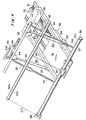
- the rear end of the board supporting body 50 can be pulled up, with the handle 60 in hand.
- the board supporting body 50 is raised, rotating about the shaft 48.
- the latch mechanism of the stay 65 operates so that the stay 65 stretches. Consequently, the board supporting body 50 is held in its obliquely raised state, as shown in Fig. 4 .
- the latch mechanism of the stay 65 is released, whereby the board supporting body 50 is returned to the horizontal position as shown in Fig. 2 .
- the magnetic sensor 47 cannot detect the permanent magnet 46.
- a keyboard 14 for inspection and an emergency stop switch 15 are further put on the base 10.
- the keyboard 14 and the switch 15 are connected to a controller, as described later.
- the keyboard 14 for inspection and the emergency stop switch 15 are used in inspecting a PC board.
- a mouse and a keyboard for teaching are put on the base 10.
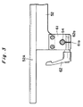
- the guide 67 is a hollow prism (rectangular in cross section), and the shaft 66 is inserted into the guide 67 from an opening end of the guide 67 (an end on the opposite side of the base end, which is attached to the bracket 63, of the guide 67).
- the guide 67 is formed with an opening 67a in the vicinity of the opening end on a side surface thereof.
- a stopper 68 having four claws is rotatably provided at the base end of the shaft 66 (an end on the opposite side of the top end, which is attached to the bracket 64, of the shaft 66).
- the guide 67 is provided with a projection 69 outside of the stopper 68, and the projection 69 is projected into the guide 67.
- the stopper 68 and the projection 69 constitute a latch mechanism.
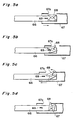
- the stay 65 operates, as shown in Figs. 5a to 5d .
- the stopper 68 rotates in a counterclockwise direction in contact with the projection 69, and one of the claws of the stopper 68 is projected outward from the opening 67a (the guide 67 can not move rightward from this position) ( Fig. 5b ).
- the claw projected outward from the opening 67a is brought into contact with an edge of the opening 67a, whereby the stopper 68 rotates in a counterclockwise direction ( Fig. 5c ).
- One of the claws of the stopper 68 and the adjacent claws are respectively brought into contact with the edge of the opening 67a and the inner surface of the guide 67, whereby the guide 67 can not further move leftward from this position (the shaft 66 can not move rightward) ( Fig. 5d ). Consequently, the board supporting body 50 is kept in its obliquely raised position.
- a ring-shaped fluorescent lamp 71 is arranged in the upper portion of a cylindrical case 79 inside thereof.
- the fluorescent lamp 71 is covered with a cover 79a.
- a ring-shaped photoconductor (made of acrylic, for example) 72 is provided below the fluorescent lamp 71.
- the inner peripheral surface of the photoconductor 72 is formed in a three-stepped shape. The portion of the uppermost step is the thickest and the lower the position is, the thinner the portion becomes. This peripheral surface of the photoconductor 72 is also in a ring shape.
- a red (R) color filer 73, a green (G) color filter 74, and a blue (B) color filter 75 are respectively positioned on the lower surface of the uppermost step, the lower surface of the middle step and the lower surface of the photoconductor 72.
- Diffusing plates 76 having slops are respectively arranged inside of the color filters 73 to 75.
- a black ring-shaped wall 77 is provided between the upper and lower diffusing plates 76.
- the color filters 73 to 75 are also in a ring shape, and the diffusing plates 76 are also in a ring shape.
- the R filter 73, the diffusing plate 76, the ring-shaped wall 77, the G filter 74, the diffusing plate 76, the ring-shaped wall 77, the B filter 75, and the diffusing plate 76 are successively fitted, and a stop ring 78 is finally screwed into the case 79, whereby the inner peripheral surface of the light projecting device 70 is assembled.
- Light emitted from the fluorescent lamp 71 passes through the photoconductor 72, to reach the R, G and B color filters 73 to 75, where the light is converted into R light, G light and B light, and the R light, G light and B light are diffused by the diffusing plates 76 and are directed downward.
- the R light, G light and B light projected downward through the color filters 73 to 75 differ in the angle of projection.
- ⁇ 3, ⁇ 2 and ⁇ 1 be angles formed by a horizontal surface of an object positioned just below the center of the light projecting device 70 (which coincides with the center of an imaging device 80) and the directions of projection of the R light, G light and B light, respectively, the relationship of ⁇ 3 > ⁇ 2 > ⁇ 1 holds.
- An image formed by light reflected from the object is picked up by the imaging device 80 positioned just above the object.
- the red reflected light is the strongest of the light incident on the imaging device.
- the larger the angle of inclination of the surface of the object from the horizontal surface is, the stronger the reflected green light and blue reflected light become.
- the angles of inclination of the surface of the object are thus represented in different colors on the image picked up.
- the emission spectrum of the fluorescent lamp, the transmission rates of the color filters 73 to 75, and the like are so determined that the R light, G light and B light are mixed to generate white light.
- the imaging device 80 is fixed to the upper portion in the center of the light projecting device 70, and comprises a zoom lens system (a lens cylinder) 81 and a camera head 82.
- the camera head 82 includes a CCD (solid state electronic imagig device).
- the zoom lens system 81 causes light reflected from an object positioned just below the zoom lens system 81 to be formed on the CCD of the camera head 82.
- the zoom magnification can be manually changed.
- Fig. 8 illustrates another example of the construction of a light projecting device.
- Fig. 9 illustrates the construction of a light source equipment.
- An imaging device is the same as the above described one.
- a light projecting device 90 there are provided no color filters and fluorescent lamp.
- Three optical fiber cables 93 to 95 are introduced into the light projecting device 90 from a light source equipment 91. Each of the optical fiber cables 93 to 95 is obtained by bundling a lot of fine optical fibers and coating the periphery thereof.
- the optical fiber cable 93 is for introducing red light, and a lot of optical fibers 93A thereof are arranged at a predetermined spacing in a ring shape so that their tips (light is projected from the tips) are positioned above the diffusing plate 76 in the uppermost step.
- the optical fiber cables 94 and 95 are for respectively introducing green light and blue light, and a lot of optical fibers 94A of the cable 94 and a lot of optical fibers 95A of the cable 95 are respectively arranged at a predetermined spacing in a ring shape so that their tips are positioned above the diffusing plates 76 in the middle step and the lower step. Even such the light projecting device 90 is used, it is possible to illuminate an object just below the light projecting device 90 at different angles and in different colors.
- halogen lamps (light sources) 92 are arranged in the light source equipment 91, and the light sources 92 are shielded from each other by partition walls 98.
- Heat preventing glass 96 and color filters (R, G, B) 73, 74 and 75 are respectively arranged ahead of the light sources 92.
- Connectors 97 of the optical fiber cables are further respectively provided ahead of the color filters 73 to 75.
- the optical fiber cables 93 to 95 are respectively inserted into the connectors 97 and are fixed by screws 97a, so that the R light, G light and B light are respectively introduced into the optical fiber cables 93, 94 and 95.
- the light source equipment 91 has features that the optical fiber cables 93 to 95 can be respectively connected to the arbitrary connectors 97. Consequently, the angles of projection of the R light, G light and B light in the light projecting device 90 can be switched. For example, if the optical fiber cable 93 is connected to the connector 97 ahead of the blue color filter 75, the blue light can be projected at the greatest angle ⁇ 3 from a position in the uppermost step in the light projecting device 90.
- the light projecting device 90 can be also changed into a light projecting device of two colors or one color by omitting one or two optical fiber cables.
- the intensities of light emission of the three light sources 92 are electrically controlled, whereby the intensities of the R light, G light and B light projected in the light projecting device 90 can be so adjusted that the R light, G light and B light are mixed to generate white light.
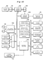
- Fig. 10 illustrates an example of the electrical construction of the visual inspection supporting apparatus.
- the visual inspection supporting apparatus is controlled by a computer system.
- the main body of a computer including a CPU to be the heart of the computer system is illustrated as a controller 100.
- Interface circuits for connecting input/output devices shall be included in the controller 100 as required.
- the visual inspection supporting apparatus has mainly the teaching mode and the inspection mode. Even in either one of the modes, performed are the driving of the X-axis table 20 and the Y-axis table 30, the imaging of the PC board PCB, the displaying of an image obtained by the imaging, and so on.
- the camera head 82 of the imaging device 80 includes a color CCD serving as an imaging device as described above, and circuits such as a circuit for processing a video signal outputted from the CCD (circuits for white balance adjustment, and gamma correction, a matrix circuit for producing R, G and B signals, and the like).
- the video signal outputted from the camera head 82 is converted into digital image data (generally, R, G and B image data) in an A/D converter (comprising three A/D converters for R, G.and B) 101.
- the digital image data are stored once in a frame memory 102.
- the digital image data read out from the frame memory 102 are converted into an analog video signal by a D/A converter 103.
- the analog video signal is fed to a CRT display device 13 through a display control circuit 104.
- the frame memory 102 can write and read out data simultaneously, and an image picked up by the camera head 82 is always displayed on the display device 13.
- the display control circuit 104 produces image data representing a cursor, a mark as described later, a display of layout on the entire PC board, a scale and the like, and displays the image data one over the other on a screen of the display device 13 under the control of the controller 100.
- the X-axis motor 29 and the Y-axis motor 39 are controlled by a XY table controller 105 on the basis of a command of the controller 100.
- the current position of the X-axis table 20 and more precisely, the X-coordinate of the center of the visual field of the imaging device 80 mounted on the X stage 21 is detected by an X position sensor 106.
- the current position of the Y-axis table 30, that is, the Y-coordinate of the center of the visual field of the imaging device 80 is detected by a Y position sensor 107.
- the position sensors 106 and 107 are, for example, rotary transducers, and are mounted on the rotational shafts of the X-axis table 20 and the Y-axis table 30, for example, the rotational shaft of the motor 29 or the shaft of the pulley 31.
- An X position signal representing the X-coordinate outputted from the X position sensor 106, a Y position signal representing the Y-coordinate outputted from the Y position sensor 107, and a detection signal outputted from the magnetic sensor 47 and indicating that the board supporting body 50 is in its horizontal position are inputted to the controller 100 via an interface 108.
- the turning-on or -off of the power supply of the light projecting device 70 is also controlled by the controller 100.
- a mouse 111 and a keyboard 112 for teaching are used for entering various data and commands.
- the mouse 111 is for designating the position and the size of a cursor, a mark or the like displayed on the CRT display device 13.
- the teaching keyboard 112 includes a key for entering a command to move the X-axis table 20 and the Y-axis table 30 (hereinafter collectively referred to as an XY table) in addition to keys for entering the board name, the board size, the zoom magnification, and the confirmation of entry.
- the inspecting keyboard 14 and the emergency stop switch 15 are used for entering various data and commands.
- the teaching keyboard 112 is also used as required.
- the inspecting keyboard 14 is provided with keys such as a key for moving a mark on a display screen (the preceding point and the succeeding point), a key for moving the XY table to the preceding or succeeding inspection area (the preceding inspection area and the succeeding inspection area), a key for moving the XY table back and forth and rightward and leftward, a key for entering a code representing unacceptable soldering, a draw command key for issuing a command to draw out the Y stage 41 forward (toward a worker), and a return key for entering a command to return the Y stage 41 to the original position.
- the emergency stop switch 15 is depressed in driving the XY table. That is, the XY table is not moved even if a movement command is entered from the inspecting keyboard 14, unless the switch 15 is turned on. This is for the purpose of safety of work (the worker cannot move the XY table without using his or her both hands).
- a memory 109 accompanied to the controller 100 is provided with an area storing image data representing an image indicating a standard (or on the limit) soldered state of a part mounted on a reference PC board, an area storing a teaching table created in the teaching processing as described later, an area storing an inspection-result table produced in the inspecting processing, an area storing a position to which the Y stage 41 is to be returned before being drawn out (a return position), an area storing the current position (the X and Y coordinates) of the XY table, a working area, and other areas.
- the teaching table created in the teaching processing and the inspection-result table produced in the inspecting processing are stored in a floppy disk or are printed out after the termination of the processing.
- a floppy disk (FD) drive 113 and a printer 114 are connected to the controller 100 in order to save and output the data.
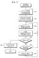
- Fig. 11 shows operations in the teaching mode (teaching processing) in the visual inspection supporting apparatus.
- the teaching processing is mainly supervised by the controller 100.
- Fig. 12 shows one example of the teaching table produced in the teaching processing.
- a reference PC board to which parts are suitably soldered is used.
- the reference PC board is first set in the receiving steps 51a and 52a of the supporting arms 51A and 52A of the board supporting body 50.
- the board name (the type name representing the type of board, the number and the like) and the board size of the reference PC board are entered from the teaching keyboard 112 (step 201).
- the board size is useful in providing a display of layout on the PC board.
- the XY table is positioned at its initial position (step 202).
- the initial position is a position where a predetermined location, for example, the lower left corner of the PC board set in the board supporting body 50 is positioned in the center of the visual field (field of vision) of the imaging device 80.
- the entire PC board does not generally enter in the visual field of the imaging device 80. Therefore, the entire PC board is divided into a plurality of areas each corresponding to a visual field. The range corresponding to one visual field becomes one inspection area.
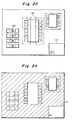
- Fig. 13 illustrates an example of a PC board PCB. A lot of parts are mounted on the PC board and soldered thereto. The range of one visual field is indicated by a one-dot and dash line. A range indicated by "IA1" is a first inspection area, and a range indicated by "IA2" is a second inspection area. If an image is enlarged by the zoom lens system 81, an inspection area is narrowed, as an eighth inspection area indicated by "IA8". Such an inspection area is designated by an inspector (a worker). The inspection areas are consecutively numbered starting with 1 so that they are distinguished.
- the visual field of the imaging device 80 is the first inspection area IA1.
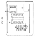
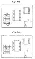
- An example of an image displayed on the screen of the display device 13 at this time is illustrated in Fig. 14 .
- the contour of the entire PC board PCB and the position of the first inspection area IA1 in the contour are displayed at the lower right portion of the screen. This is a layout display LD.
- the inspector views such a display screen to designate a portion whose soldering is to be inspected (a designated point) (step 203).
- the point to be inspected can be designated using various marks.
- a part to be inspected can be designated with a circular mark, as indicated by a circle mark MC.
- a zone to be inspected can be designated, put in a frame, as indicated by a frame mark MF.
- the circle mark MC or the frame mark MF need not necessarily correspond to one part. It is possible to indicate a plurality of parts by one mark. Alternatively, it is also possible to divide one part into a plurality of zones and indicate the zones by a plurality of marks.
- the circle mark MC or the frame mark MF is produced by the display control circuit 104 in response to a command from the teaching keyboard 112 or the mouse 111, and is displayed on the display screen with a particular color superimposed thereon.
- the size of the circle of the circle mark MC and the size of the frame of the frame mark MF are variable by the command from the mouse 111.
- the inspector successively designates points to be inspected using the mark MC or MF while seeing an image of a part displayed on the display screen.
- the designated points are assigned designation numbers (serial numbers) in the order designated.
- the designated points are stored in the teaching table (step 204).
- the teaching table includes the entered board name and board size stored therein, and includes for each inspection area number the coordinates representing the position of an inspection area corresponding thereto and data relating to points designated in the inspection area.
- the coordinates of the inspection area are the coordinates of a particular point of the inspection area, for example, a point at the lower left corner.
- the data relating to the designated point comprises a designation number and the position of a designated point corresponding thereto (coordinate data).
- Data representing the position of the designated point is constituted by a code representing the type of mark (MC or MF), the diameter and the coordinates (the X and Y coordinates) of the center of the mark in the case of the circle mark MC, or the length and breadth of the mark and the coordinates of the center of the mark in the case of the frame mark MF. If the coordinates of the inspection area and the zoom magnification are found, the coordinates in the XY table of an arbitrary point on the screen are uniquely determined. The controller 100 calculates the coordinates of the center, the diameter or the length of the side of the designated mark on the basis of the position on the screen of the mark.
- an electrode (a lead) E of a part, a land L on the PC board, and soldered areas R, G and B indicated in colors are indicated only with respect to one part. This is also substantially the same in the other drawings of the display screen.
- the inspector enters a command to move the XY table from the teaching keyboard 112, to position the succeeding inspection area (steps 206 and 207).
- the succeeding inspection area may be partially overlapped with or spaced apart from the preceding inspection area. The inspector may determine the succeeding inspection area on his or her judgment.
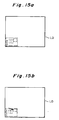
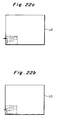
- a layout display image representing the succeeding inspection area appears in the layout display LD.
- the layout display LD may be expressed by an inspection area and designated marks, as shown in Fig. 15a , a mark finally designated may be indicated by an arrow as shown in Fig. 15b , or the current inspection area may be indicated by an arrow.
- all the inspection areas and the points which have been designated are displayed in the layout display LD. Consequently, the inspector can know to what extent the inspection areas and the points are designated. Particularly if the inspection area which has already been designated and the inspection area which is being currently designated are displayed in different forms (in different colors, for example), they are easier to understand.
- the inspector successively designates portions to be inspected (inspection areas and points) on the PC board without omission.
- the processing in the steps 203 and 204 is also repeated with respect to the succeeding inspection area.
- the same processing is repeated while successively positioning a new inspection area (steps 206 and 207).
- the produced teaching table is saved in the floppy disk FD by the FD drive 113 in response to entry indicating that the operations and processing have been terminated by the inspector (step 208).
- the zoom magnification is fixed at a constant value.
- the zoom magnification is stored in the teaching table in conformity with the board name.
- the zoom magnification will be entered from the keyboard 112.
- the zoom magnification need not be keyed. At this time, the zoom magnification is not also stored in the teaching table.
- the zoom magnification may be varied for each inspection area. In this case, the size of the inspection area varies depending on the zoom magnification, as described above.
- the zoom magnification is entered prior to designating a point to be inspected (step 203).
- the zoom magnification is stored in the teaching table in conformity with an inspection area number.
- the zoom magnification may be entered for each designated point.
- a command to store an image may be enterable from the keyboard 112 when a point to be inspected is designated.
- an image in the vicinity of a part designated by a mark is extracted, and the extracted image data is stored in an image data area, linking to an inspection area number and a designation number.
- the image data may be stored in the teaching table.
- the image data thus extracted, along with the teaching table, is saved in the floppy disk FD as one representing a standard image (or a limit image).
- the designation number may be replaced with the entered part name in the teaching table.
- the visual inspection supporting apparatus can be used for the inspector to inspect a PC board (a PC board to be inspected) for acceptability of soldering in the inspection mode, and can be also used for the inspector to immediately correct a soldered portion which is judged to be unacceptable. For convenience, a case where a plurality of PC boards are only inspected and a case where they are corrected will be separately described.
- Figs. 16 to 18 show the procedure for processing in a case where only inspection is made. This processing is also mainly supervised by the controller 100.
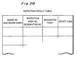
- Fig. 20 shows an example of an inspection-result table.
- a plurality of PC boards of the same type are successively inspected.
- a floppy disk FD storing a teaching table for the PC boards of the type to be inspected is set in the FD drive 113.
- the board name (the type of board) of the PC board to be inspected is entered from the teaching keyboard 112 (or the inspecting keyboard 14) (step 211).
- the plurality of PC boards to be inspected have the same name.
- board numbers are assigned to the PC boards. A number previously assigned to each of the PC boards can be used as the board number. In this case, when the PC board is set (step 213), the board number is entered.
- the apparatus may automatically assign the board numbers starting with 1 in the order inspected. In this case, the PC boards which have been inspected must be so preserved that the order of inspection can be found (they are numbered or stacked).
- the teaching table designated by the board name is read out from the floppy disk FD, and the teaching table is stored in the memory 109 (step 212).
- the inspector sets the PC board PCB to be inspected in the board supporting body 50 (step 213).
- the controller 100 refers to the teaching table (particularly, the coordinates of inspection areas) read in the memory 109, to move the XY table to the position where the first inspection area (No. 1) is imaged (step 214). Consequently, an image of the inspection area No. 1 is displayed on the display screen of the display device 13.
- the inspector judges whether or not soldering on the PC board is acceptable while seeing the displayed image with his or her own eyes. An acceptable soldered portion is not entered, while only a soldered portion which is judged to be unacceptable, along with a code indicating the particulars of its defect (fault), is entered.
- a soldered portion to be inspected is designated using a mark as described above in teaching processing, and a designation mark is also superimposed on a displayed image of a PC board to be inspected, the inspector may follow a portion to be inspected with his or her eyes with the help of the designation mark. Since data relating to the designation mark is stored in the teaching table, the designation mark is displayed by the display controller 104 on the basis of the data.
- a method of displaying a designation mark is mainly divided into three types.
- the three types are the mark manually forwarding mode, the automatically forwarding mode, and the inspection-area manually fowarding mode.
- the inspector uses the inspecting keyboard 14 (or the teaching keyboard 112), to select any one of these modes (step 215).
- a circle mark MC of a designation number 1 is first displayed, as shown in Fig. 21a , on an image on a display screen (an image of an inspection area No. 1).
- the inspector judges whether or not soldering of a part on which the circle mark MC is put (in the case of a frame mark MF, a zone circumscribed by the frame mark MF) is acceptable by seeing the displayed image. If soldering is acceptable, the inspector depresses the succeeding point key on the inspecting keyboard 14 (step 221). Consequently, a mark MC of a designation number 2 is displayed on the display screen, as shown in Fig. 21b (step 222).
- the inspector successively forwards the mark (the circle mark MC or the frame mark MF) while successively depressing the succeeding point key, to judge whether or not soldering of a portion to be inspected which is indicated by the mark is acceptable.
- the mark is displayed on the basis of the data relating to the designated point in the teaching table.
- the inspector depresses the preceding point key (step 219). Consequently, the mark of the preceding designation number is displayed again (step 220) (return from display shown in Fig. 21b to display shown in Fig. 21a , for example).
- a layout display LD on the display screen the position on the PC board of an inspection area currently displayed is indicated by an arrow.
- a portion on the PC board where a mark is displayed appears on the layout display, as shown in Figs. 22a and 22b.
- Fig. 22a and Fig. 22b respectively correspond to Figs. 21a and Fig. 21b .
- the inspector Upon finding out an unacceptable soldered portion, the inspector depresses a defect code key representing its defect found out on the inspecting keyboard 14 (step 227).
- the defect code include "no soldering", “excessive soldering", “a bridge”, and "a missing part (no part)".
- a defect code When the defect code is entered, a board number for identifying a PC board undergoing inspection (the board name as required), an inspection area number representing an area being inspected, a designation number representing a portion where a defect is found out, the coordinates of the designation number (a designated point : a code, the diameter or the length and breadth, and the center coordinates), and the defect code are registered in the inspection-result table (step 228) (see Fig. 20 ).
- an unacceptable portion may be explicitly indicated by changing the color or the shape of a mark (MC, MF) for designating the portion which is judged to be unacceptable. It is preferable that the mark representing the unacceptable portion is not erased until the display of the succeeding inspection area is started.
- the unacceptable portion may be displayed in the layout display LD.
- the particulars of the entered defect code may be displayed in characters on the display screen to urge the inspector to confirm the defect code. It is preferable that the defect code which has been entered once can be canceled as required.
- the inspector depresses the succeeding inspection area key (step 225), whereby the XY table is so driven that the succeeding inspection area No. 2 can be imaged by referring to data representing the coordinates of inspection areas in the teaching table (step 226).
- the inspector repeats the above described operations. It is thus possible to perform soldering inspection of all designated points in all inspection areas which are registered in the teaching table.
- the XY table is so driven that the preceding inspection area is imaged by the imaging device 80 (step 224).
- a displayed mark MC or MF successively moves on the screen in order of designation numbers at predetermined time intervals (step 217).
- the inspector judges whether or not soldering of a portion represented by the mark is acceptable while successively following the displayed mark.
- the inspector Upon finding out unacceptable soldering, the inspector depresses the defect code key in the same manner as described above, whereby data relating to the unacceptable soldering is registered in the inspection-result table (steps 227 and 228).
- the inspection of the succeeding inspection area is started by depressing the succeeding inspection area key, as described above (steps 225 and 226).
- the time interval during which a displayed mark moves may be predetermined. Alternatively, the inspector can also enter the time interval using the keyboard 14 or 112.
- a stop key is previously provided in the inspecting keyboard 14 so that a displayed mark is fixed not to move when the stop key is depressed. Consequently, the inspector can carefully inspect a particular portion.
- all marks MC and MF belonging to an area to be inspected are displayed once and for all, as shown in Fig. 23 (step 218).
- the inspector visually inspects all portions to be inspected while following the marks with his or her eyes.
- the inspector Upon finding out an unacceptable portion, the inspector points a cursor (displayed on the display screen) at a mark indicating an unacceptable portion, to specify the unacceptable portion and keys a defect code.
- the color or the shape of the displayed mark may be successively changed every time the inspector depresses the succeeding point key so that the inspector can indicate a defective (faulty) point.
- designation numbers may be displayed adjacent to the marks so that the inspector can key-input a designation number of a defective point. In any case, a point which is judged to be defective and a defect code are registered in the inspection-result table.
- the inspector depresses the succeeding inspection area key on the inspecting keyboard 14 (step 225). Consequently, the imaging device 80 and the Y stage 41 are so moved that the succeeding inspection area can be imaged (step 226). Thereafter, all the marks MC and MF belonging to the set inspection area are displayed once and for all. The inspector can thus perform visual inspection for each inspection area.
- the inspector takes out a PC board having been inspected from the board supporting body 50 (step 231), and sets the succeeding PC board to be inspected (step 231), after which soldering inspection is performed in the same manner.
- step 232 When inspection of all PC boards to be inspected which are previously prepared is completed (step 232), the contents of the inspection-result table are saved in the floppy disk FD.
- a statistical operation is executed and the result of the operation is displayed. Specifically, when the inspector enters an operation command from the keyboard 14 or 112, a total or statistical operation effective in analyzing the quality of mounting is executed using data representing the result of inspection of all PC boards which have already been inspected, and the result of the operation is displayed on the display device 13 and is saved in the floppy disk FD.
- Examples of the total or statistical operation include a rate of defect relating to PC boards (a value obtained by dividing the number of defective PC boards by the number of all PC boards), a rate of defect related to parts (a value obtained by dividing the number of defective parts by the number of all parts), a rate of defect for each type of part, the order of defective items for each type of part, and the order of defective portions starting with the most defective portion and the particulars of the defect.
- the result of the inspection and the result of the operation are printed out from the printer 114 as required.
- Fig. 24 illustrates another method of displaying a portion to be inspected (particularly in the mark manually forwarding mode and the automatically forwarding mode).
- the brightness in an area of a portion to be inspected (the inside of a frame mark MF) is made different from the brightness of the other areas (for example, the inside of the frame mark MF is made bright) instead of circumscribing the portion to be inspected by the frame mark MF.
- the portion to be inspected is indicated by an arrow.
- all areas which are circumscribed by frame marks will be so displayed that the brightness of the areas differs from the brightness of the other areas.
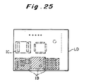
- Fig. 25 illustrates another example of a layout display LD.
- this layout display LD an area which has already been inspected is displayed in a form different from those in the other area (by changing the brightness and the color of the area which has already been inspected, as indicated by "IB").
- An area being currently inspected is also displayed so that it can be found that the area is being currently inspected, as indicated by "IC" (by circumscribing the area by a frame, changing the brightness or the color of the area, for example).
- the zoom magnification is fixed.
- the zoom magnification is displayed on the display device 13.
- the inspector sees the display of the zoom magnification to adjust the zoom lens system 81 by hand so that the displayed zoom magnification is realized.
- the zoom magnification is displayed on the display device 13 every time the inspection area is changed (step 226), whereby the inspector adjusts the zoom lens system 81 by hand so that the displayed zoom magnification is realized.
- the standard image (a limit image) of a part designated by a mark MC (or MF) is displayed on a display screen, as shown in Fig. 26 (in Fig. 26 , the standard image is displayed at the upper left portion).
- the inspector can compare the standard image (one in which soldering is acceptable or one in which soldering is just in the boundary between acceptable and unacceptable) with an image designated by the mark to judge whether or not soldering in the image designated by the mark is acceptable.
- the visual inspection supporting apparatus comprises a marking unit
- the inspector can enter a marking command upon finding out unacceptable soldering. Since the marking unit is moved to an unacceptable soldered portion on a PC board which is pointed out by the inspector, where ink is dropped on the unacceptable soldered portion, the unacceptable portion is indicated on the actual PC board.
- Fig. 27 illustrates another example of a display.
- a scale SC is displayed near a part, a portion or a location being cuurently inspected which is indicated by a mark MC.
- the inspector can judge whether or not soldering is acceptable by referring to the scale SC. Particularly, it is judged whether or not soldering at the tip of a lead (an electrode) is acceptable depending on whether or not a fillet (a portion indicated in blue B on a display screen) is correctly formed. It is judged whether or not soldering is acceptable by measuring the length of the filet using the scale SC (that will be described later with reference to Figs. 30a and 30b ).
- the zoom magnification is determined, the length on the display screen can be converted, whereby the scale SC is displayed on the basis of the zoom magnification.
- the zoom magnification is fixed, the fixed zoom magnification is used.
- the zoom magnification is entered, the entered zoom magnification is used.
- the zoom magnification is detected as described later (see Fig. 35 ), the detected zoom magnification is used. This is also the same in the other examples of a display as described later.
- the personal difference between inspectors is made up by thus displaying the scale, whereby it is possible to objectively and accurately make judgment and make the quality of inspection constant. In addition, the operating efficiency is improved.
- Fig. 28 two cursors CU1 and CU2 are displayed on a display screen so that the cursors can be moved using the mouse 111.
- the inspector aligns the cursors CU1 and CU2 with both ends of a fillet (one end is normally the tip of a lead).
- the distance between the two cursors is calculated using the zoom magnification and is displayed. The labor of the inspector can be further reduced, and the operating efficiency is improved.
- Fig. 29 illustrates still another example of a display, in which a portion of a display screen is illustrated in enlarged form.
- the distance between two cursors is displayed as a measured value, and a standard value or a boundary value (the criterion in inspection) is also displayed. The objective judgment is further ensured.
- Fig. 30a illustrates a cross section of a part PA, a lead (an electrode) E, solder SO, a land L, and a PC board PCB
- Fig. 30b illustrates a photographed image thereof.
- a portion having a steep slope in the solder SO is indicated in blue B, and a portion having a gentle slope is indicated in green G (see the construction of the above described light projecting device 70 or 90).
- the portion indicated in blue B is referred to as a fillet.
- Figs. 31 and 32 illustrate still another example of a display, in which the fillet length and the fillet area are automatically measured, respectively.
- a window W is set to a portion to be inspected by the inspector. The position and the size of the window W will be determined using the mouse 111 by the inspector.
- a color signal B representing a blue color out of signals representing the three primary colors which are obtained from the imaging device 80 is used.
- the maximum value of the length in the horizontal direction (the number of pixels) in which the color signal B has a value of not less than a predetermined threshold value represents the fillet length.
- the number of pixels in which the color signal B has a value of not less than a predetermined threshold value represents the fillet area.
- the fillet area will be represented utilizing the number of pixels, square millimeter or the like as a unit.
- the fillet length and the fillet area are thus automatically found and are displayed, thereby improving the operating efficiency.
- the soldered state can be represented by a numerical value by calculating the ratio of the portion in blue B to the portion in red R (the length ratio and the area ratio) and the ratio of the portion in green G to the portion in red R.
- the area and the length of the portion in red R are significantly larger than those of the portions in the other colors in a case where the solder SO is small in amount and is almost perpendicularly attached.
- the area and the length of the portion in green G are increased in a case where the solder SO is small in amount and is almost horizontally attached. The soldered state can be found depending on which of portions in the colors is the largest.
- the inspector Upon finding out unacceptable soldering, the inspector enters its defective point and a defect code representing its defect as described above, whereby data representing the defect are stored in the inspection-result table (steps 227 and 228).
- the inspector then draws out the PC board, along with the Y stage 41, toward himself or herself to manually correct an unacceptable portion by hand.
- a board draw command from the keyboard 14 or 112 (step 234)
- the positions of the X stage 21 and the Y stage 41 (the coordinates of the center of the visual field) at that time are stored as return positions in the memory 109, and the display screen is frozen (steps 235 and 236).
- an image of an inspection area at that time is displayed as a still image by repeatedly reading out the same image data from the frame memory 102.
- the Y stage 41 is fed forward (nearer to the inspector) to the leading end of the rail 33 along the Y-axis rail 33 (step 237).
- the inspector obliquely raises the board supporting body 50 with the handle 60 in his or her hand. Consequently, the PC board PCB disposed on the board supporting body 50 is inclined. In this state, the inspector searches for an unacceptable soldered portion on the PC board while referring to the layout display LD on the display screen and the frozen image, to correct unacceptable soldering using a soldering iron (step 288).
- the inspector When the correction of unacceptable soldering is completed, the inspector returns the board supporting body 50 to its horizontal position and provide entry indicating that unacceptable soldering has been corrected from the keyboard 14 (step 239). After it is confirmed that the magnetic sensor 47 detects the permanent magnet 46 (step 240), the Y stage 41 is returned to the stored return position (step 241). The freezing of the displayed image is released (step 242). The fact that unacceptable soldering has been corrected is stored in the inspection-result table in conformity with its defective point.
- the inspector can correct the unacceptable portion in a state where the PC board PCB is drawn out toward himself or herself and is obliquely raised. Moreover, the image of the inspection area continues to be frozen and displayed even after the PC board PCB is drawn out, whereby the inspector can easily find out the unacceptable portion on the PC board.
- the inspector may mark the unacceptable portion instead of correcting unacceptable soldering.
- correcting work in the step 234 and the subsequent steps can be performed after inspection of one inspection area is completed or inspection of one PC board is completed.
- soldering correction can be made in the above described manner by setting only a PC board having an unacceptable portion on the board supporting body 50 after the inspection of all PC boards is completed.
- Fig. 35 illustrates another example of the electrical construction of the visual inspection supporting apparatus.
- the same blocks as those shown in Fig. 10 are assigned the same reference numerals and hence, the description thereof is not repeated.
- a zoom lens driver 115 for moving a zoom lens of the zoom lens system 81 in accordance with a command from a controller 100 and a zoom position sensor 116 for sensing the position of the zoom lens.
- a zoom position signal of the sensor 116 is fed to the controller 100.
- a position command value given to the zoom lens driver 115 can be also used as zoom lens position data without providing the sensor 116. In either case, the zoom magnification is determined by the position of the zoom lens.
- the light source equipment 91 shown in Fig. 9 is connected to the controller 100 in place of the light projecting device 70.
- the zoom magnification can be determined for each type of board or for each inspection area by entering a zoom command from a keyboard 112 in teaching processing.
- the zoom magnification is stored in a teaching table.
- the zoom magnification may be designated for each part (designated point). In this case, the zoom magnification is stored for each designation number in the teaching table.
- the zoom lens is automatically driven by the zoom lens driver 115 for each type of board, for each inspection area, or for each part (point) in accordance with the zoom magnification stored in the teaching table, and the designated zoom magnification is realized.
- the zoom magnification may be also used for displaying the scale, calculating the length and calculating the area shown in Figs. 27 to 32 .
- Figs. 36 to 40 illustrate another example of the mechanical construction of the visual inspection supporting apparatus.
- a base 10, a table 11, an X-axis table 20, a light projecting device 70, and an imaging device 80 are the same as those shown in Fig. 1 and hence, the illustration thereof is omitted.
- Fig. 36 corresponds to Fig. 2 , which illustrates a Y-axis table 120.
- Figs. 36 to 40 the same members, elements or portions as those shown in Figs. 1 to 4 (including those not only having the same shape but also performing the same or similar function) are assigned the same reference numerals to avoid overlapping of description as much as possible.
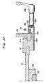
- a guide member 121 is fixed to the front half of the Y stage 41 (a supporting plate 43) on both sides thereof, and a guide groove 121a is horizontally formed along the longitudinal direction of the guide member 121 on an outer side surface thereof (particularly see Fig. 37 ).
- a guide and lock plate 122 is fixed to the lower surface of the guide member 121.
- the guide and lock plate 122 extends outward and is raised upward at its outer end.
- a screw hole 122a is formed at the front portion of a raised portion.
- a attaching piece 124 is fixed to the rear end of the Y stage 41.
- the attaching piece 124 is provided with a magnetic sensor 125.
- the front end of a Y-axis rail 33 is raised to serve as stopper 33a.
- the peculiar construction in the present embodiment is that a sliding member 130 is provided.
- the sliding member 130 has sliding walls 131 provided on both sides thereof.
- a rail 131a extending in the longitudinal direction is formed inside of the sliding walls 131.
- the rail 131a is slidably fitted in the guide groove 121a of the guide member 121. Consequently, the sliding member 130 is slidable back and forth with respect to the Y stage 41.
- the right and left sliding walls 131 are fixedly coupled to each other by a front plate 51 of the board supporting member 50 and a cover 134 fixedly laid over the sliding walls 131.
- An auxiliary plate 132 extending in the longitudinal direction is fixedly attached to the sliding wall 131 outside thereof.
- the auxiliary plate 132 extends outward and is curved downward.
- a downwardly curved portion of the auxiliary plate 132 is formed with a long hole 133 extending in the longitudinal direction.
- a fixing lever 136 has a screw 136a fixed thereto and axially projected (particularly see Fig. 37 ). The screw 136a is screwed in the screw hole 122a of the guide and lock plate 122 through the long hole 133.
- the rail 131a inside of the sliding walls 131 is formed with a raised stopper 131b at the rear end thereof.
- the stopper 131b abuts against the rear end of the guide member 121 of the Y stage 41, to determine the limit of forward draw of the sliding member 130 (see Fig. 40 ).
- a stopper 137 is secured on the front portion of the sliding walls 131 inside thereof to project inward. When the sliding member 130 retreats, the stopper 137 abuts against a projection 41a provided on the front end surface of the stage 41. Consequently, the retreat position of the sliding member 130 is determined. In the normal state (at the time of inspecting a PC board), the sliding member 130 is in this retreat position.
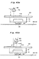
- the present embodiment is the same as the above described embodiment in that the board supporting body 50 comprises a front plate 51 and a rear plate 53 which are linked by rods 54, and a movable plate 52 which is movable along the rods 54.
- the board supporting body 50 is mounted on not the Y stage 41 but the sliding member 130 so as to be capable of being raised and laid down. That is, the front plate 51 of the board supporting body 50 is pivoted at both lower portion thereof to the front portions of the sliding walls 131 of the sliding member 130 by shafts 48.
- One of the sliding walls 131 of the sliding member 130 is formed with a hole 135 is provided at the front portion thereof (particularly see Fig. 38 ).
- a bolt 145 passes through the hole 135.
- a bracket 142 bent at right angles is secured to a portion, which corresponds to the hole 135, of the board supporting body 50, and a arc-shaped long hole 143 is formed on a forwardly projected portion of the bracket 142.
- the bolt 145 is screwed into a lever 141 through the arc-shaped long hole 143.
- a handle 147 is attached to the front plate 51 via a bracket 146.
- Two split pieces 61 through which the two rods 54 are respectively inserted are fixedly attached to the rear surface of the movable plate 52.
- the split pieces 61 are respectively formed with holes so as to horizontally intersect slits 61a of the split pieces 61, and a clamp screw bar 148 passes through the holes (particularly see Fig. 39 ).
- the screw bar 148 passes through a spacing holding pipe 149 between the two split pieces 61.
- a clamp 150 and a cap 151 each having a female screw formed therein are respectively screwed to both ends, which are extended outward from the split pieces 61, of the screw bar 148. Consequently, the two split pieces 61 respectively fasten the rods 54 by turning the clamp 150.
- a permanent magnet 152 is attached to a location, which corresponds to the magnetic sensor 125, of the rear plate 53.
- the permanent magnet 152 is detected by the sensor 125 only in a case where the sliding member 130 is in its retreat position and the board supporting body 50 is in its horizontal position.
- the Y-axis table of such construction is used similarly to that in the above described embodiment in the teaching mode and the inspection mode. At this time, the sliding member 130 is held in the retreat position and the board supporting body 50 is held in the horizontal position.
- a method of using the Y-axis table differs from that in the above described embodiment only when an unacceptable soldered portion on the PC board is corrected. It is assumed that a predetermined inspection area on a PC board PCB is imaged by the imaging device 80, and an image obtained by the imaging is displayed on a display device 13. When the unacceptable soldered portion on the PC board is corrected in this state, the inspector loosens the lever 136 to draw out the sliding member 130 forward while holding the Y stage 41 in its position. Unacceptable soldering is corrected in a state where the board supporting body 50 is obliquely raised (see Fig. 40 ).
- the inspector After the correcting work of unacceptable soldering, the inspector returns the board supporting body 50 to the horizontal position and returns the sliding member 130 to the original retreat position. Since this state is sensed by the sensor 125, the driving of the Y stage 41 by a motor 39 is allowed.
- Fig. 41 illustrates still another example of the construction of the Y-axis table.
- a rotating base 160 is rotatably provided on a Y stage 41.
- a board supporting body 50 is disposed on the rotating base 160.
- the board supporting body 50 is rotated in a horizontal plane to rotate the PC board, to facilitate correcting work of an unacceptable soldered portion of the part.
- a supporting plate 161 is fixed to the Y stage 41. through an intermediate plate 165.
- the supporting plate 161 is provided with a cross-roller bearing 162.
- a positioning ring 164 and a shaft 163 are fixed to the lower surface of the rotating base 160.
- V grooves 164A and 164B are formed at angular intervals of 90° in the positioning ring 164.
- the V groove indicated by "164B" out of the V grooves is deeper than the other V groove 164A, which represents the position of the origin.
- the shaft 163 is rotatably received by the bearing 162, whereby the rotating base 160 is rotatably supported on the Y stage 41.
- An arm 166 is rotatably pivoted at its one end on the supporting plate 161 through a shaft 168, a thrust bearing 169 and a bush 170.
- a lever 167 is fixed to the base end of the arm 166.
- a cam follower 171 is rotatably mounted on an approximately middle point of the arm 166.
- a spring (a helical tension spring) 173 is provided between a pin 172 standing on the supporting plate 161 and a spring post 174 at the top end of the arm 166. Consequently, the top end of the arm 166 is urged by the spring 173, so that the cam follower 171 is brought into contact with the peripheral surface of the positioning ring 164 or is fitted in the V groove 164A or 164B.
- the rotating base 160 is positioned in four positions where the cam follower 171 is fitted in the V groove 164A or 164B.
- the cam follower 171 When the rotating base 160 is rotated, the cam follower 171 may be drawn out of the V groove 164A or 164B against the urging force of the spring 173 by means of the lever 167 to rotate the rotating base 160 by hand.
- a proximity switch 175 is mounted on the supporting base 161 by a bracket 176.
- an object 177 to be detected of the proximity switch 175 is mounted on the top end of the arm 166.
- the proximity switch 175 outputs a detection signal only at this time. Consequently, it is recognized that the rotating base 160 is in the position of the origin by the detection signal of the proximity switch 175.
- the driving of the Y stage 41 may be allowed on the basis of this detection signal.
- the board supporting body 50 can be also provided on the rotating base 160 so as to be capable of being raised and laid down as required.
- a Y-axis table base 181 is swingably supported on an apparatus base 180 by a pivot shaft 182.
- the pivot shaft 182 coincides with a moving path of a light projecting device 70 and an imaging device 80. Specifically, the shaft 182 is positioned just below the center VC of the view of field of the imaging device 80.
- a rail 33 is provided on the base 181, and a Y stage 41 is moved along the rail 33.
- a board supporting body 50 for supporting a PC board PCB is fixedly provided on the Y stage 41.
- a motor 183 for swing is positioned at the rear of the apparatus base 180, and a timing belt 186 is reeved around a pulley 185 fixed to the rotational shaft of the motor 183 and a pulley 184 rotatably provided above the pulley 185.
- the timing belt 186 is linked to an attaching piece 187 provided for the base 181 at a portion thereof.
- the base 181 is inclined, as shown in Fig. 42b , by rotating the motor 183. It is thus possible to observe an area to be detected on the PC board PCB through the imaging device 80 in a state where the PC board PCB is inclined.
- the center VC of the visual field moves, as indicated by "VC1", by inclining the base 181.
- the Y stage 41 is slightly moved (backward in this example). Letting h and ⁇ be the height from the center of the shaft 182 to the PC board PCB and the angle of inclination of the base 181, respectively, the Y stage 41 may be moved by a distance of h ⁇ sin ⁇ . Since the height h is a fixed value and the angle of inclination ⁇ can be calculated from the amount of rotation of the motor 183, the Y stage 41 can be automatically moved.
- Figs. 43a and 43b relate to an X-axis table, which is so adapted as to incline the light projecting device 70 and the imaging device 80.
- the Y stage 41 travels on the swinging base 181 or the fixed base 10.
- the visual field of the imaging device 80 is shifted by a distance of h ⁇ sin ⁇ , where h is the distance between an image forming surface of the imaging device 80 and the PC board PCB. Therefore, an X stage is moved by the above amount of the shift in order to compensate for the shift of the visual field.
- Fig. 44 illustrates a mechanism for inclining the light projecting device 70 and the imaging device 80.
- the light projecting device 70 and the imaging device 80 are fixed to a mounting plate 191.
- a shaft 192 is fixed to the mounting plate 191.
- the shaft 192 is rotatably supported by the X stage 21.
- a pulley 195 is fixed to the shaft 192.
- a motor 193 is mounted on the X stage 21, and a pulley 194 is fixed to the rotational shaft of the motor 193.
- a timing belt 196 is reeved around the pulleys 194 and 195.
- the light projecting device 70 and the imaging device 80 can be inclined at an arbitrary angle in an arbitrary direction by rotating the motor 193 in the forward and reverse directions.
- the movement of the X stage 21 depends on the motor 29, as described above.
- the inspector enters a designated point representing a point to be inspected from a keyboard
- the designated point can be also determined using position data representing a part to be mounted which is stored in a CAD system for designing a PC board, or position data representing a position where a part is to be mounted or of a soldered portion which are held by a part mounting apparatus for mounting a part on a PC board.
- position data representing a position where a part is to be mounted or of a soldered portion which are held by a part mounting apparatus for mounting a part on a PC board.
- all positions represented by the existing data or its groups may be taken as designated points.
- the position data, along with an image may be displayed on a display screen, to make the inspector select any of the position data.
- the board supporting body is so constructed that it is pivoted at its front end and is raised by pulling up its rear end
- the board supporting body may be pivoted in the middle position between the front end and the rear end thereof.
- the board supporting body can be also brought into its raised state (inclined state) by pivoting the board supporting body at its rear end and lowering its front end.
- the apparatus may set an inspection area.
- the number of inspection areas into which a PC board should be divided is calculated based on the size of the PC board and the size of the visual field of the imaging device. If the number of inspection areas is determined, an XY table is so controlled that the visual field is successively set in the respective divided inspection areas. Teaching processing is performed for each visual field (inspection area).
- Fig. 45 illustrates an example of the construction of a system utilizing the above described visual inspection supporting apparatus as a soldering correcting apparatus.
- An automatic PC board inspecting apparatus 301 judges whether or not soldering on a PC board is acceptable, to produce data representing the result of inspection.
- the inspection result data includes at least a PC board ID, position data representing an unacceptable portion, a defect code.
- the inspection result data is sent to a data collecting apparatus 302.
- the data collecting apparatus 302 stores the inspection result data in a floppy disk FD, and sends the inspection result data to a soldering correcting apparatus 303 online or via a server 304.
- the inspection result data stored in the floppy disk FD is read by the soldering correcting apparatus 303.
- soldering correcting apparatus 303 when a defective PC board is set in an XY table and the PC board ID is entered, the XY table is so controlled that an area including an unacceptable soldered portion is imaged on the basis of the pertinent inspection result data. An image picked-up is displayed on a display device. The displayed image is frozen. A correction worker draws out the PC board toward himself or herself and corrects unacceptable soldering on the PC board while seeing the displayed image.
- the PC board ID can be also entered by the worker.
- a bar code expressed on the PC board may be read by a bar code reader connected to the data collecting apparatus 302 and transmitted to the soldering correcting apparatus 303 from the data collecting apparatus 302.
Abstract
Description
- The present invention relates to a visual inspection supporting apparatus which is used for an inspector to visually inspect acceptability of soldering of electronic parts mounted on a printed circuit board, and the use of said apparatus for correcting an unacceptable soldered portion during manufacture of a printed circuit board.
- In this type of apparatus called by various names, for example, a visual inspection supporting apparatus, a printed circuit board inspecting apparatus, an automatic printed circuit board inspecting apparatus, and an external appearance inspecting apparatus, light sources of the three primary colors, i.e., red (R), green (G) and blue (B) are generally used. The light sources are so arranged as to project illuminating light at different angles to a portion to be inspected. When the portion to be inspected is imaged by an imaging device and an image obtained by the imaging is displayed, inclined surfaces or flat surfaces having different angles are indicated in different colors. Consequently, color information can be also utilized for judging whether or not soldering is acceptable.
- Various proposals have been made in such a direction as to automate judgment whether or not soldering is acceptable. Examples include a proposal for a illuminating method (see Japanese Patent Application Laid-Open Publication No.
4-355311 4-343046 - However, there are not many devises and proposals from the viewpoint of assisting an inspector in visual inspection. It is highly important to increase the operation (work) efficiency of the inspector and ensure more objective judgment which is not dependent on the personal difference between inspectors. Particularly, the visual inspection has the advantage that when an unacceptable soldered portion is found out, the unacceptable soldered portion can be immediately corrected. It has been desired to realize a suitable apparatus for supporting such visual inspection.
-
EP 0 413 817 A1 - In
US 5,204,912 a viewing assembly is mounted on a XY-movement device for scanning the viewing assembly parallel to a table supporting a PCB to be inspected. -
US 4,832,250 A discloses a semi-automated electronic circuit board rework and repair system, comprising a table movable along guide rods of a plate in y-direction, wherein the plate is movable on guide rods in x-direction. -
US 4,566,325 A discloses an inspection board for PCBs. Aplaten 50 is slidably supported on guide rods which are attached to support blocks. The support blocks are slidably attached to guide rails. Guide rails and supports form a frame which is pivotably attached to a base, e.g. the lower edge is hinged to the base. Further the base can be a light table with a light transmitting top. - An object of the present invention is to provide a supporting apparatus for PCB visual inspection and correction of an unacceptable portion which makes it easy for an inspector to perform work and makes it possible to improve operation (work) efficiency.
- Another object of the present invention is to provide a visual inspection supporting apparatus capable of ensuring the objectivity of judgment by an inspector.
- The apparatus of the present invention can be developed into not only support of visual inspection but also automatic inspection.
- The invention is defined in
claims 1 and 24, respectively. - Particular embodiments of the invention are set out in the dependent claims.
- Using the visual inspection supporting apparatus according to the present invention allows to judge whether or not soldering on a printed circuit board is acceptable and to correct a soldered portion which is judged to be unacceptable.
- A visual inspection supporting apparatus according to the present invention comprises a illuminating device for illuminating a printed circuit board to be inspected, an imaging device for imaging an area on the board illuminated by the illuminating device and outputting an image signal representing an image obtained by the imaging, a stage which is movable relatively to the illuminating device and the imaging device in two perpendicular directions, a board supporting member supported on the stage for supporting the board to be inspected, and a mechanism for moving the stage until the board supported on the board supporting member reaches a position outside of a range in which the illuminating device and the imaging device exist.
- There is generally provided a display device for displaying the image represented by the image signal outputted from the imaging device.
- The visual inspection supporting apparatus is suitable for not only inspection but also correction of an unacceptable portion. Since the board supported on the stage is drawn out of the range in which the illuminating device and the imaging device exist, it is possible to correct the unacceptable portion at the position where the board is drawn out.
- The board supporting member is rotatably supported on the stage so as to be capable of being obliquely raised and laid down, and provided is a mechanism for holding the board supporting member in its obliquely raised position.
- Since the unacceptable portion can be corrected on the obliquely raised board, it becomes easy for the inspector to perform correcting work.
- The image obtained by the imaging before the stage is drawn out is frozen and is displayed as a still image on the display device. The inspector can search for the unacceptable portion on the board by seeing the image.
- Since the board, along with the movable body, can be drawn out even by using this apparatus, it becomes easy to perform correcting work of an unacceptable portion. Consequently, the apparatus is suitable for soldering inspection and correction of a part having a lead on four perpendicular sides.
- The visual inspection supporting apparatus further comprises storage means for storing previously taught position data representing a point to be inspected on a board to be inspected and display control means for performing control so as to indicate the point to be inspected on the image displayed on the display device in accordance with the position data stored in the storage means.
- Consequently, a portion to be inspected is indicated, thereby improving the operating efficiency of the inspection.
- The result of the inspection is immediately entered from an input device. A portion which is judged to be unacceptable as the result of the inspection is indicated on a screen of the display device.
- More preferably, a layout display indicating the position on the board of an area of the image displayed on the display device is provided. Consequently, the inspector can find an area currently inspected, and can also grasp the progress of the inspection.
- In order to make up the personal difference between inspectors to ensure objectivity, a scale for expressing the length is displayed on the image displayed on the display device.
- Furthermore, two lines are movably displayed on the display screen of the display device, and the spacing between the two lines is calculated and is displayed.
- Additionally, a window is displayed on the display screen of the display device, and data relating to the size of a particular image in the window is displayed. More preferably, data relating to the reference size is displayed in addition to the data relating to the size of the particular image.
- The other features of the present invention will become more apparent from embodiments explained hereinbelow.
-
-
Figs. 1 to 4 illustrate an example of the mechanical construction of a visual inspection supporting apparatus (Part 1), -
Fig. 1 is a perspective view of the entire apparatus, -
Fig. 2 is a perspective view showing a Y-axis table in enlarged form, -
Fig. 3 is a cross-sectional view showing in enlarged form a portion for fixing a movable plate, -
Fig. 4 is a perspective view showing a state where a board supporting member is raised; -
Figs. 5a to 5d andFigs. 6a to 6d are cross-sectional views showing the construction and the operation of a stay for holding a board supporting member in its raised state; -
Fig. 7 is a cross-sectional view showing the construction of a light projecting device and an imaging device (Part 1); -
Fig. 8 is a cross-sectional view showing the construction of a light projecting device and an imaging device (Part 2); -
Fig. 9 illustrates the construction of a light source equipment to which the light projecting device shown inFig. 8 is connected; -
Fig. 10 is a block diagram showing the electrical construction of the visual inspection supporting apparatus (Part 1); -
Fig. 11 is a flow chart showing the procedure for teaching processing; -
Fig. 12 illustrates an example of a teaching table; -
Fig. 13 is a plan view showing one example of a printed circuit board; -
Fig. 14 illustrates an example of an image displayed in teaching processing; -
Figs. 15a and 15b illustrate examples of a layout display; -
Figs. 16 ,17 ,18 and19 are flow charts showing the procedure for inspecting processing and correcting processing; -
Fig. 20 illustrates an example of an inspection-result table; -
Figs. 21a and 21b show how a mark representing a designated point is successively driven; -
Figs. 22a and 22b show how a layout display is changed; -
Fig. 23 illustrates an example of an image in which marks representing all designated points in one inspection area are displayed once and for all; -
Fig. 24 illustrates another example in which a designated point is indicated; -
Fig. 25 illustrates another example of a layout display; -
Fig. 26 illustrates an example in which a standard image is displayed; -
Fig. 27 illustrates an example in which a scale is displayed on an image; -
Fig. 28 illustrates an example in which two lines are displayed on an image; -
Fig. 29 illustrates an example in which the measured fillet length, along with the criterion in inspection, is displayed; -
Fig. 30a is a cross-sectional view showing a lead, solder and a land, andFig. 30b illustrates an image corresponding thereto; -
Fig. 31 illustrates an example of a display in a case where the fillet length is automatically measured; -
Fig. 32 illustrates an example of a display in a case where the fillet area is automatically measured; -
Figs. 33a and 34a are cross-sectional views showing solder and its vicinity, andFigs. 33b and 34b illustrate an example of a displayed image corresponding thereto; -
Fig. 35 is a block diagram showing the electrical construction of the visual inspection supporting apparatus (Part 2); -
Figs. 36 to 40 illustrate an example of the mechanical construction of the visual inspection supporting apparatus (Part 2), -
Fig. 36 is an enlarged perspective view of a Y-axis table, -
Fig. 37 is an enlarged cross-sectional view taken along a line VII - VII shown inFig. 36 , -
Fig. 38 is an enlarged cross-sectional view taken along a line VIII - VIII shown inFig. 36 , -
Fig. 39 is an enlarged cross-sectional view taken along a line IX - IX shown inFig. 36 , and -
Fig. 40 is a perspective view showing a state where a board supporting member is raised; -
Fig. 41 is an exploded perspective view showing an example of the mechanical construction of the visual inspection supporting apparatus (Part 3); -
Figs. 42a and 42b illustrate a structure for inclining a Y table base; -
Figs. 43a to 43b illustrate a structure for inclining a light projecting device and an imaging device; -
Fig. 44 is an enlarged perspective view of an X stage; and -
Fig. 45 is a block diagram showing a system in which a soldering correcting apparatus is combined with an automatic board inspecting apparatus. - An example of the mechanical construction of a visual inspection supporting apparatus for assisting in work for visually inspecting a printed circuit (PC) board on which parts are mounted for acceptability of soldering is illustrated in
Figs. 1 to 4 . - A printed circuit board on which electronic parts are mounted is generally manufactured through a mounting step for disposing and positioning an electronic part (hereinafter merely referred to as a "part") on a printed circuit board (hereinafter merely referred to as a "PC board" or "board"), a soldering step using soldering methods such as a flow soldering method and a reflow soldering method, a soldering inspecting step for judging whether or not soldering is acceptable, and a soldering correcting step for correcting a soldered portion which is judged to be unacceptable. No soldering correcting step is, of course, required with respect to a PC board having no unacceptable soldered portion. The soldering step and the subsequent steps may, in some cases, be performed again with respect to a PC board having a soldered portion difficult or impossible to correct.
- The visual inspection supporting apparatus is used for either one or both of the soldering inspecting step and the soldering correcting step. That is, the visual inspection supporting apparatus is used for assisting an inspector (a worker) in performing work for visually inspecting a soldered portion on a PC board for acceptability and assisting a worker (an inspector) in performing manual work for correcting an unacceptable soldered portion. As apparent from the following, an unacceptable portion can be corrected after visual inspection of one or a plurality of PC boards is completed, and an unacceptable portion can be also corrected every time the unacceptable portion is found out in visual inspection of one PC board.
- Particularly referring to
Figs. 1 and2 , a fixed table 11 is positioned on the rear half of abase 10, andlegs 12 of the table 11 are secured to thebase 10. The upper surface of the table 11 is higher in position than the base 10, and aCRT display device 13 is disposed on the upper surface of the table 11. - An X-axis table 20 is provided along the front edge of the table 11. In addition, a Y-axis table 30 is provided on the base 10 in such an arrangement as to perpendicularly cross the X-axis table 20. The X-axis table 20 moves in the X-axis direction and positions a light projecting
device 70 and animaging device 80. The Y-axis table 30 moves in the Y-axis direction and positions a PC board PCB. - The X-axis table 20 is mounted on the lower surface of the front edge of the table 11, and comprises an
X-axis rail 23 and a supportingrail 24 extending in the transverse direction (the X-axis direction). AnX stage 21 is provided with aslider 22. Theslider 22 is slidably fitted to theX-axis rail 23. A portion including theslider 22 of theX stage 21 is slidably supported on the supportingrail 24. - An
endless timing belt 25 is disposed along theX-axis rail 23. Thetiming belt 25 is reeved around pulleys (gears) 27 and 28 each having teeth on its peripheral surface. Thepulley 27 is rotatably mounted on the lower surface of the table 11 at one end thereof, and thepulley 28 is fixed to the rotational shaft of an X-axis motor (a DC motor) 29. Themotor 29 is fixed to the lower surface of the table 11. Thetiming belt 25 is attached to theX stage 21 at its one portion. - By driving the
motor 29, theX stage 21 is moved rightward and leftward along theX-axis rail 23 via thetiming belt 25 and is placed in an arbitrary position. The light projectingdevice 70 and theimaging device 80 are mounted on theX stage 21. - The Y-axis table 30 comprises a Y-
axis rail 33 secured to thebase 10. The Y-axis rail 33 perpendicularly crosses theX-axis rail 23. -
A Y stage 41 comprises a supportingplate 43, a slidingmember 42 fixed to the lower surface of the supportingplate 43,side members 44 formed integrally with the supportingplate 43 on both sides thereof and extending in the longitudinal direction (the Y-axis direction), and arear member 45 fixed between the rear ends of theside members 44. The slidingmember 42 is slidably fitted to the Y-axis rail 33. - An
endless timing belt 35 is disposed along the Y-axis rail 33. Pulleys (gears) 37 and 38 each having teeth formed on its peripheral surface are rotatably provided at the front end and the rear end of thebase 10, respectively. Thetiming belt 35 is reeved around thepulleys timing belt 35 is attached to abracket 43a fixed to the lower surface of the supportingplate 43. - A
pulley 31 and thepulley 38 at the rear of the base 10 are secured to a common shaft. On the other hand, apulley 36 is fixed to the rotational shaft of a Y-axis motor (a DC motor) 39. Atiming belt 32 is reeved around thepulleys pulleys motor 39 are fixed to thebase 10 by a fixing member (not shown). - A
frame 34 is provided around the Y-axis rail 33 and thetiming belt 35. Theframe 34 is fixed to thebase 10. Astopper 34a and astopper 34b are respectively fixed to the front end and the rear end of theframe 34. Thestoppers Y stage 41. A cover (not shown) is attached to theframe 34 in such a manner as not to prevent the movement of theY stage 41. - By driving the Y-
axis motor 39, theY stage 41 is moved back and forth along therail 33 via thetiming belts - A
board supporting body 50 is mounted on theY stage 41 so as to be capable of being raised and laid down. Theboard supporting body 50 comprises afront plate 51, amovable plate 52, arear plate 53, androds 54. Each of thefront plate 51 and themovable plate 52 has leg portions extending downward from both ends thereof. Supportingarms front plate 51 and themovable plate 52, respectively. Therear plate 53 has leg portions extending downward from both ends thereof. The leg portions of thefront plate 51 and the leg portions of therear plate 53 are respectively connected by therods 54. Both ends of therod 54 are respectively fixed to the leg portions of thefront plate 51 and therear plate 53. -
Cylinders 55 are perpendicularly fixed to the leg portions of themovable plate 52, respectively. The leg portions of themovable plate 52 are respectively provided with holes corresponding to through holes of thecylinders 55. Therods 54 slidably pass through the through holes of thecylinders 55 and the holes of the leg portions, respectively. Consequently, themovable plate 52 is movable along therods 54 between the front andrear plates - As shown in
Fig. 3 , asplitted piece 61 is fixedly attached to one of the leg portions of themovable plate 52, on a surface opposite to the surface where thecylinder 55 is mounted, of themovable plate 52. Thesplitted piece 61 also has a hole through which therod 54 slidably passes, and a slit 61a is formed downward from the hole. A screw hole is formed in a direction perpendicular to the slit 61a, and ascrew 62a integrally secured to alever 62 is fitted in the screw hole. Thescrew 62a is screwed in the screw hole by means of thelever 62, whereby the hole of thesplitted piece 61 is reduced in size to tighten therod 54. Consequently, themovable plate 52 is fixed. - Receiving
steps 51a and 52a are respectively formed on the upper portions of the supportingarms front plate 51 and themovable plate 52 at inside thereof along the longitudinal direction of the supporting arms. A receivingpiece 58 and abracket 59 are, respectively, fixedly attached to one end and the other end of the supportingarm 51A of thefront plate 51, and ashaft 57 is fixed at both ends thereof to the receivingpiece 58 and thebracket 59. Theshaft 57 is parallel to the supportingarm 51A with small spacing. Apressing piece 56 is slidably and rotatably mounted on theshaft 57. - The PC board PCB is received between the receiving step 51a of the supporting
arm 51A and the receivingstep 52a of the supportingarm 52A. The position of themovable plate 52 is so adjusted that the PC board PCB just stays between the receivingsteps 51a and 52a, and themovable plate 52 is fixed by means of thelever 62. The PC board PCB is brought leftward and is placed in a position abutting against the receivingpiece 58. Thepressing piece 56 is moved to a position abutting against the right end of the PC board PCB. A permanent magnet is embedded in the front end of thepressing piece 56, and thefront plate 51 is formed of a magnetic material (for example, iron). If thepressing piece 56 is moved along theshaft 57 in a state where it is raised as indicated by a one-dot and dash line inFig. 2 , and is laid down in the position abutting against the right end of the PC board PCB, the permanent magnet attracts thefront plate 51, whereby thepressing piece 56 is fixed. The PC board PCB is fixed in a state where it is received by the receivingsteps 51a and 52a and put between the receivingsteps 51a and 52a and between the receivingpiece 58 and thepressing piece 56. If thefront plate 51 is not formed of a magnetic material, a magnetic plate may be fixedly attached along the supportingarm 51A. - The
front plate 51 of theboard supporting body 50 is attached at both leg portions thereof rotatably (so as to be capable of being raised and laid down) to the front ends of theside members 44 of theY stage 41 byshafts 48. In a state where theboard supporting body 50 is laid down (a state shown inFig. 2 ), ablock 53A fixed to the rear side of therear plate 53 of theboard supporting body 50 abuts against and is received by therear member 45 of theY stage 41. Ahandle 60 extending upward is mounted on theblock 53A, and apermanent magnet 46 is embedded in the lower surface of theblock 53A. On the other hand, a magnetic sensor (for example, a Hall element) 47 is embedded, at a location, which corresponds to thepermanent magnet 46, in therear member 45 of theY stage 41. If theboard supporting body 50 is in the state shown inFig. 2 , themagnetic sensor 47 detects thepermanent magnet 46, to output a detection signal. Consequently, it is possible to recognize that theboard supporting body 50 is in its laid position (horizontal position). It goes without saying that the magnetic sensor may be replaced with another sensor (a limit switch or the like). -
Brackets 63 are fixedly attached to the front portions of theside members 44 of theY stage 41 andbrackets 64 are attached to the leg portions of therear plate 53 of theboard supporting body 50. Astay 65 comprises aguide 67, ashaft 66 removably inserted into theguide 67, and a latch mechanism for fixing theshaft 66 to a predetermined position of theguide 67. The base end of theguide 67 of thestay 65 and the top end of theshaft 66 are pivoted on thebracket 63 and thebracket 64, respectively. - The rear end of the
board supporting body 50 can be pulled up, with thehandle 60 in hand. Theboard supporting body 50 is raised, rotating about theshaft 48. After theboard supporting body 50 is pulled up to a suitable height, the end thereof is slightly lowered, then the latch mechanism of thestay 65 operates so that thestay 65 stretches. Consequently, theboard supporting body 50 is held in its obliquely raised state, as shown inFig. 4 . - Thereafter, when the rear end of the
board supporting body 50 is slightly pulled up by means of thehandle 60, the latch mechanism of thestay 65 is released, whereby theboard supporting body 50 is returned to the horizontal position as shown inFig. 2 . In a state where theboard supporting body 50 is obliquely raised, themagnetic sensor 47 cannot detect thepermanent magnet 46. - In
Fig. 1 , akeyboard 14 for inspection and anemergency stop switch 15 are further put on thebase 10. Thekeyboard 14 and theswitch 15 are connected to a controller, as described later. Thekeyboard 14 for inspection and theemergency stop switch 15 are used in inspecting a PC board. When a teaching operation as described later is performed, a mouse and a keyboard for teaching are put on thebase 10. - Although the construction of the
stay 65 functioning as described above has already been known, the construction and the function will be briefly described with reference toFigs. 5a to 5d andFigs. 6a to 6d . - In
Fig. 5a , theguide 67 is a hollow prism (rectangular in cross section), and theshaft 66 is inserted into theguide 67 from an opening end of the guide 67 (an end on the opposite side of the base end, which is attached to thebracket 63, of the guide 67). Theguide 67 is formed with anopening 67a in the vicinity of the opening end on a side surface thereof. Astopper 68 having four claws is rotatably provided at the base end of the shaft 66 (an end on the opposite side of the top end, which is attached to thebracket 64, of the shaft 66). In addition, theguide 67 is provided with aprojection 69 outside of thestopper 68, and theprojection 69 is projected into theguide 67. Thestopper 68 and theprojection 69 constitute a latch mechanism. - In a process for obliquely raising the
board supporting body 50 from its laid position, thestay 65 operates, as shown inFigs. 5a to 5d . When theguide 67 moves rightward (theshaft 66 moves leftward), thestopper 68 rotates in a counterclockwise direction in contact with theprojection 69, and one of the claws of thestopper 68 is projected outward from theopening 67a (theguide 67 can not move rightward from this position) (Fig. 5b ). When theguide 67 is returned leftward, the claw projected outward from theopening 67a is brought into contact with an edge of theopening 67a, whereby thestopper 68 rotates in a counterclockwise direction (Fig. 5c ). One of the claws of thestopper 68 and the adjacent claws are respectively brought into contact with the edge of theopening 67a and the inner surface of theguide 67, whereby theguide 67 can not further move leftward from this position (theshaft 66 can not move rightward) (Fig. 5d ). Consequently, theboard supporting body 50 is kept in its obliquely raised position. - When the
board supporting body 50 is slightly pulled up, thehandle 60 in hand as described above, the latch mechanism is released, whereby theboard supporting body 50 is returned to the horizontal position. This process is illustrated inFigs. 6a to 6d . - When the
guide 67 moves rightward from the state ofFig. 5d , thestopper 68 abuts against theprojection 69 to rotate in a counterclockwise direction (Figs. 6a to 6b ) (theguide 67 can not further move rightward from this position). When theguide 67 then moves leftward, the claw of thestopper 68 projected outward from theopening 67a abuts against the edge of theopening 67a, whereby thestopper 68 rotates in a counterclockwise direction, to enter the guide 67 (Fig. 6c ). In this state, theguide 67 can move leftward (theshaft 66 can move rightward) (Fig. 6d ). - An example of the construction of a light projecting
device 70 will be described with reference toFig. 7 . A ring-shapedfluorescent lamp 71 is arranged in the upper portion of acylindrical case 79 inside thereof. Thefluorescent lamp 71 is covered with acover 79a. A ring-shaped photoconductor (made of acrylic, for example) 72 is provided below thefluorescent lamp 71. The inner peripheral surface of thephotoconductor 72 is formed in a three-stepped shape. The portion of the uppermost step is the thickest and the lower the position is, the thinner the portion becomes. This peripheral surface of thephotoconductor 72 is also in a ring shape. - A red (R)
color filer 73, a green (G)color filter 74, and a blue (B)color filter 75 are respectively positioned on the lower surface of the uppermost step, the lower surface of the middle step and the lower surface of thephotoconductor 72. Diffusingplates 76 having slops are respectively arranged inside of thecolor filters 73 to 75. A black ring-shapedwall 77 is provided between the upper andlower diffusing plates 76. The color filters 73 to 75 are also in a ring shape, and the diffusingplates 76 are also in a ring shape. TheR filter 73, the diffusingplate 76, the ring-shapedwall 77, theG filter 74, the diffusingplate 76, the ring-shapedwall 77, theB filter 75, and the diffusingplate 76 are successively fitted, and astop ring 78 is finally screwed into thecase 79, whereby the inner peripheral surface of the light projectingdevice 70 is assembled. - Light emitted from the
fluorescent lamp 71 passes through thephotoconductor 72, to reach the R, G andB color filters 73 to 75, where the light is converted into R light, G light and B light, and the R light, G light and B light are diffused by the diffusingplates 76 and are directed downward. The R light, G light and B light projected downward through thecolor filters 73 to 75 differ in the angle of projection. Letting θ3, θ2 and θ1 be angles formed by a horizontal surface of an object positioned just below the center of the light projecting device 70 (which coincides with the center of an imaging device 80) and the directions of projection of the R light, G light and B light, respectively, the relationship of θ3 > θ2 > θ1 holds. An image formed by light reflected from the object is picked up by theimaging device 80 positioned just above the object. When the surface of the object is near to horizontal, the red reflected light is the strongest of the light incident on the imaging device. The larger the angle of inclination of the surface of the object from the horizontal surface is, the stronger the reflected green light and blue reflected light become. The angles of inclination of the surface of the object are thus represented in different colors on the image picked up. - Preferably, the emission spectrum of the fluorescent lamp, the transmission rates of the
color filters 73 to 75, and the like are so determined that the R light, G light and B light are mixed to generate white light. - The
imaging device 80 is fixed to the upper portion in the center of the light projectingdevice 70, and comprises a zoom lens system (a lens cylinder) 81 and acamera head 82. Thecamera head 82 includes a CCD (solid state electronic imagig device). Thezoom lens system 81 causes light reflected from an object positioned just below thezoom lens system 81 to be formed on the CCD of thecamera head 82. The zoom magnification can be manually changed. -
Fig. 8 illustrates another example of the construction of a light projecting device.Fig. 9 illustrates the construction of a light source equipment. An imaging device is the same as the above described one. - In a light projecting
device 90, there are provided no color filters and fluorescent lamp. Threeoptical fiber cables 93 to 95 are introduced into the light projectingdevice 90 from alight source equipment 91. Each of theoptical fiber cables 93 to 95 is obtained by bundling a lot of fine optical fibers and coating the periphery thereof. Theoptical fiber cable 93 is for introducing red light, and a lot ofoptical fibers 93A thereof are arranged at a predetermined spacing in a ring shape so that their tips (light is projected from the tips) are positioned above the diffusingplate 76 in the uppermost step. Similarly, theoptical fiber cables optical fibers 94A of thecable 94 and a lot ofoptical fibers 95A of thecable 95 are respectively arranged at a predetermined spacing in a ring shape so that their tips are positioned above the diffusingplates 76 in the middle step and the lower step. Even such thelight projecting device 90 is used, it is possible to illuminate an object just below thelight projecting device 90 at different angles and in different colors. - In
Fig. 9 , three halogen lamps (light sources) 92 are arranged in thelight source equipment 91, and thelight sources 92 are shielded from each other bypartition walls 98. Heat preventingglass 96 and color filters (R, G,B) light sources 92.Connectors 97 of the optical fiber cables are further respectively provided ahead of thecolor filters 73 to 75. Theoptical fiber cables 93 to 95 are respectively inserted into theconnectors 97 and are fixed byscrews 97a, so that the R light, G light and B light are respectively introduced into theoptical fiber cables - The
light source equipment 91 has features that theoptical fiber cables 93 to 95 can be respectively connected to thearbitrary connectors 97. Consequently, the angles of projection of the R light, G light and B light in the light projectingdevice 90 can be switched. For example, if theoptical fiber cable 93 is connected to theconnector 97 ahead of theblue color filter 75, the blue light can be projected at the greatest angle θ3 from a position in the uppermost step in the light projectingdevice 90. The light projectingdevice 90 can be also changed into a light projecting device of two colors or one color by omitting one or two optical fiber cables. - Furthermore, the intensities of light emission of the three
light sources 92 are electrically controlled, whereby the intensities of the R light, G light and B light projected in the light projectingdevice 90 can be so adjusted that the R light, G light and B light are mixed to generate white light. -
Fig. 10 illustrates an example of the electrical construction of the visual inspection supporting apparatus. The visual inspection supporting apparatus is controlled by a computer system. The main body of a computer including a CPU to be the heart of the computer system is illustrated as acontroller 100. Interface circuits for connecting input/output devices shall be included in thecontroller 100 as required. - The visual inspection supporting apparatus has mainly the teaching mode and the inspection mode. Even in either one of the modes, performed are the driving of the X-axis table 20 and the Y-axis table 30, the imaging of the PC board PCB, the displaying of an image obtained by the imaging, and so on.
- The
camera head 82 of theimaging device 80 includes a color CCD serving as an imaging device as described above, and circuits such as a circuit for processing a video signal outputted from the CCD (circuits for white balance adjustment, and gamma correction, a matrix circuit for producing R, G and B signals, and the like). The video signal outputted from thecamera head 82 is converted into digital image data (generally, R, G and B image data) in an A/D converter (comprising three A/D converters for R, G.and B) 101. The digital image data are stored once in aframe memory 102. The digital image data read out from theframe memory 102 are converted into an analog video signal by a D/A converter 103. The analog video signal is fed to aCRT display device 13 through adisplay control circuit 104. Preferably, theframe memory 102 can write and read out data simultaneously, and an image picked up by thecamera head 82 is always displayed on thedisplay device 13. - The
display control circuit 104 produces image data representing a cursor, a mark as described later, a display of layout on the entire PC board, a scale and the like, and displays the image data one over the other on a screen of thedisplay device 13 under the control of thecontroller 100. - The
X-axis motor 29 and the Y-axis motor 39 are controlled by aXY table controller 105 on the basis of a command of thecontroller 100. - The current position of the X-axis table 20 and more precisely, the X-coordinate of the center of the visual field of the
imaging device 80 mounted on theX stage 21 is detected by anX position sensor 106. Similarly, the current position of the Y-axis table 30, that is, the Y-coordinate of the center of the visual field of theimaging device 80 is detected by aY position sensor 107. Theposition sensors motor 29 or the shaft of thepulley 31. An X position signal representing the X-coordinate outputted from theX position sensor 106, a Y position signal representing the Y-coordinate outputted from theY position sensor 107, and a detection signal outputted from themagnetic sensor 47 and indicating that theboard supporting body 50 is in its horizontal position are inputted to thecontroller 100 via aninterface 108. The turning-on or -off of the power supply of the light projectingdevice 70 is also controlled by thecontroller 100. - In the teaching mode, a mouse 111 and a
keyboard 112 for teaching are used for entering various data and commands. The mouse 111 is for designating the position and the size of a cursor, a mark or the like displayed on theCRT display device 13. Theteaching keyboard 112 includes a key for entering a command to move the X-axis table 20 and the Y-axis table 30 (hereinafter collectively referred to as an XY table) in addition to keys for entering the board name, the board size, the zoom magnification, and the confirmation of entry. - In the inspection mode, the inspecting
keyboard 14 and theemergency stop switch 15 are used for entering various data and commands. Theteaching keyboard 112 is also used as required. The inspectingkeyboard 14 is provided with keys such as a key for moving a mark on a display screen (the preceding point and the succeeding point), a key for moving the XY table to the preceding or succeeding inspection area (the preceding inspection area and the succeeding inspection area), a key for moving the XY table back and forth and rightward and leftward, a key for entering a code representing unacceptable soldering, a draw command key for issuing a command to draw out theY stage 41 forward (toward a worker), and a return key for entering a command to return theY stage 41 to the original position. Theemergency stop switch 15 is depressed in driving the XY table. That is, the XY table is not moved even if a movement command is entered from the inspectingkeyboard 14, unless theswitch 15 is turned on. This is for the purpose of safety of work (the worker cannot move the XY table without using his or her both hands). - A
memory 109 accompanied to thecontroller 100 is provided with an area storing image data representing an image indicating a standard (or on the limit) soldered state of a part mounted on a reference PC board, an area storing a teaching table created in the teaching processing as described later, an area storing an inspection-result table produced in the inspecting processing, an area storing a position to which theY stage 41 is to be returned before being drawn out (a return position), an area storing the current position (the X and Y coordinates) of the XY table, a working area, and other areas. - The teaching table created in the teaching processing and the inspection-result table produced in the inspecting processing are stored in a floppy disk or are printed out after the termination of the processing. A floppy disk (FD) drive 113 and a
printer 114 are connected to thecontroller 100 in order to save and output the data. -
Fig. 11 shows operations in the teaching mode (teaching processing) in the visual inspection supporting apparatus. The teaching processing is mainly supervised by thecontroller 100.Fig. 12 shows one example of the teaching table produced in the teaching processing. - In the teaching mode, a reference PC board to which parts are suitably soldered is used. The reference PC board is first set in the receiving steps 51a and 52a of the supporting
arms board supporting body 50. The board name (the type name representing the type of board, the number and the like) and the board size of the reference PC board are entered from the teaching keyboard 112 (step 201). The board size is useful in providing a display of layout on the PC board. - When an initial positioning command is entered from the
teaching keyboard 112, the XY table is positioned at its initial position (step 202). The initial position is a position where a predetermined location, for example, the lower left corner of the PC board set in theboard supporting body 50 is positioned in the center of the visual field (field of vision) of theimaging device 80. - The entire PC board does not generally enter in the visual field of the
imaging device 80. Therefore, the entire PC board is divided into a plurality of areas each corresponding to a visual field. The range corresponding to one visual field becomes one inspection area. -
Fig. 13 illustrates an example of a PC board PCB. A lot of parts are mounted on the PC board and soldered thereto. The range of one visual field is indicated by a one-dot and dash line. A range indicated by "IA1" is a first inspection area, and a range indicated by "IA2" is a second inspection area. If an image is enlarged by thezoom lens system 81, an inspection area is narrowed, as an eighth inspection area indicated by "IA8". Such an inspection area is designated by an inspector (a worker). The inspection areas are consecutively numbered starting with 1 so that they are distinguished. - When the XY table is positioned at its initial position, the visual field of the
imaging device 80 is the first inspection area IA1. An example of an image displayed on the screen of thedisplay device 13 at this time is illustrated inFig. 14 . The contour of the entire PC board PCB and the position of the first inspection area IA1 in the contour are displayed at the lower right portion of the screen. This is a layout display LD. - The inspector views such a display screen to designate a portion whose soldering is to be inspected (a designated point) (step 203). The point to be inspected can be designated using various marks. For example, a part to be inspected can be designated with a circular mark, as indicated by a circle mark MC. Alternatively, a zone to be inspected can be designated, put in a frame, as indicated by a frame mark MF. The circle mark MC or the frame mark MF need not necessarily correspond to one part. It is possible to indicate a plurality of parts by one mark.
Alternatively, it is also possible to divide one part into a plurality of zones and indicate the zones by a plurality of marks. - The circle mark MC or the frame mark MF is produced by the
display control circuit 104 in response to a command from theteaching keyboard 112 or the mouse 111, and is displayed on the display screen with a particular color superimposed thereon. The size of the circle of the circle mark MC and the size of the frame of the frame mark MF are variable by the command from the mouse 111. - The inspector successively designates points to be inspected using the mark MC or MF while seeing an image of a part displayed on the display screen. The designated points are assigned designation numbers (serial numbers) in the order designated.
- When the inspector designates all points on the display screen (one inspection area) and provide entry indicating that the designation has been completed, the designated points are stored in the teaching table (step 204).
- Referring to
Fig. 12 , the teaching table includes the entered board name and board size stored therein, and includes for each inspection area number the coordinates representing the position of an inspection area corresponding thereto and data relating to points designated in the inspection area. The coordinates of the inspection area are the coordinates of a particular point of the inspection area, for example, a point at the lower left corner. The data relating to the designated point comprises a designation number and the position of a designated point corresponding thereto (coordinate data). Data representing the position of the designated point is constituted by a code representing the type of mark (MC or MF), the diameter and the coordinates (the X and Y coordinates) of the center of the mark in the case of the circle mark MC, or the length and breadth of the mark and the coordinates of the center of the mark in the case of the frame mark MF. If the coordinates of the inspection area and the zoom magnification are found, the coordinates in the XY table of an arbitrary point on the screen are uniquely determined. Thecontroller 100 calculates the coordinates of the center, the diameter or the length of the side of the designated mark on the basis of the position on the screen of the mark. - In the displayed image shown in
Fig. 14 , an electrode (a lead) E of a part, a land L on the PC board, and soldered areas R, G and B indicated in colors are indicated only with respect to one part. This is also substantially the same in the other drawings of the display screen. - When the designation of all points is completed with respect to one inspection area, the inspector enters a command to move the XY table from the
teaching keyboard 112, to position the succeeding inspection area (steps 206 and 207). The succeeding inspection area may be partially overlapped with or spaced apart from the preceding inspection area. The inspector may determine the succeeding inspection area on his or her judgment. - A layout display image representing the succeeding inspection area appears in the layout display LD. The layout display LD may be expressed by an inspection area and designated marks, as shown in
Fig. 15a , a mark finally designated may be indicated by an arrow as shown inFig. 15b , or the current inspection area may be indicated by an arrow. When the designation of points has already been completed with respect to a plurality of inspection areas, all the inspection areas and the points which have been designated are displayed in the layout display LD. Consequently, the inspector can know to what extent the inspection areas and the points are designated. Particularly if the inspection area which has already been designated and the inspection area which is being currently designated are displayed in different forms (in different colors, for example), they are easier to understand. The inspector successively designates portions to be inspected (inspection areas and points) on the PC board without omission. - The processing in the
steps steps 206 and 207). - When the foregoing operations and processing are terminated with respect to all the areas on the reference PC board set on the board supporting body 50 (step 205), the produced teaching table is saved in the floppy disk FD by the FD drive 113 in response to entry indicating that the operations and processing have been terminated by the inspector (step 208).
- In the foregoing description, the zoom magnification is fixed at a constant value. When the zoom magnification is fixed with respect to one PC board, the zoom magnification is stored in the teaching table in conformity with the board name. The zoom magnification will be entered from the
keyboard 112. - When a predetermined zoom magnification is set, the zoom magnification need not be keyed. At this time, the zoom magnification is not also stored in the teaching table.
- The zoom magnification may be varied for each inspection area. In this case, the size of the inspection area varies depending on the zoom magnification, as described above. The zoom magnification is entered prior to designating a point to be inspected (step 203). The zoom magnification is stored in the teaching table in conformity with an inspection area number. The zoom magnification may be entered for each designated point.
- Furthermore, a command to store an image may be enterable from the
keyboard 112 when a point to be inspected is designated. In this case, an image in the vicinity of a part designated by a mark is extracted, and the extracted image data is stored in an image data area, linking to an inspection area number and a designation number. The image data may be stored in the teaching table. The image data thus extracted, along with the teaching table, is saved in the floppy disk FD as one representing a standard image (or a limit image). When the inspector uses thekeyboard 112 to enter the part name in conformity with the designation number, the designation number may be replaced with the entered part name in the teaching table. - As described above, the visual inspection supporting apparatus can be used for the inspector to inspect a PC board (a PC board to be inspected) for acceptability of soldering in the inspection mode, and can be also used for the inspector to immediately correct a soldered portion which is judged to be unacceptable. For convenience, a case where a plurality of PC boards are only inspected and a case where they are corrected will be separately described.
-
Figs. 16 to 18 show the procedure for processing in a case where only inspection is made. This processing is also mainly supervised by thecontroller 100.Fig. 20 shows an example of an inspection-result table. - A plurality of PC boards of the same type are successively inspected. A floppy disk FD storing a teaching table for the PC boards of the type to be inspected is set in the FD drive 113. In addition, the board name (the type of board) of the PC board to be inspected is entered from the teaching keyboard 112 (or the inspecting keyboard 14) (step 211). The plurality of PC boards to be inspected have the same name. In order to distinguish the plurality of PC boards, board numbers are assigned to the PC boards. A number previously assigned to each of the PC boards can be used as the board number. In this case, when the PC board is set (step 213), the board number is entered. The apparatus may automatically assign the board numbers starting with 1 in the order inspected. In this case, the PC boards which have been inspected must be so preserved that the order of inspection can be found (they are numbered or stacked).
- In either case, when the board name is entered, the teaching table designated by the board name is read out from the floppy disk FD, and the teaching table is stored in the memory 109 (step 212).
- The inspector sets the PC board PCB to be inspected in the board supporting body 50 (step 213). Upon entry indicating that the PC board has been set, the
controller 100 refers to the teaching table (particularly, the coordinates of inspection areas) read in thememory 109, to move the XY table to the position where the first inspection area (No. 1) is imaged (step 214). Consequently, an image of the inspection area No. 1 is displayed on the display screen of thedisplay device 13. The inspector judges whether or not soldering on the PC board is acceptable while seeing the displayed image with his or her own eyes. An acceptable soldered portion is not entered, while only a soldered portion which is judged to be unacceptable, along with a code indicating the particulars of its defect (fault), is entered. - Since a soldered portion to be inspected is designated using a mark as described above in teaching processing, and a designation mark is also superimposed on a displayed image of a PC board to be inspected, the inspector may follow a portion to be inspected with his or her eyes with the help of the designation mark. Since data relating to the designation mark is stored in the teaching table, the designation mark is displayed by the
display controller 104 on the basis of the data. - A method of displaying a designation mark is mainly divided into three types. The three types are the mark manually forwarding mode, the automatically forwarding mode, and the inspection-area manually fowarding mode. The inspector uses the inspecting keyboard 14 (or the teaching keyboard 112), to select any one of these modes (step 215).
- When the mark manually forwarding mode is selected, a circle mark MC of a designation number 1 is first displayed, as shown in
Fig. 21a , on an image on a display screen (an image of an inspection area No. 1). The inspector judges whether or not soldering of a part on which the circle mark MC is put (in the case of a frame mark MF, a zone circumscribed by the frame mark MF) is acceptable by seeing the displayed image. If soldering is acceptable, the inspector depresses the succeeding point key on the inspecting keyboard 14 (step 221). Consequently, a mark MC of a designation number 2 is displayed on the display screen, as shown inFig. 21b (step 222). The inspector successively forwards the mark (the circle mark MC or the frame mark MF) while successively depressing the succeeding point key, to judge whether or not soldering of a portion to be inspected which is indicated by the mark is acceptable. The mark is displayed on the basis of the data relating to the designated point in the teaching table. - When it is desired to look over once again a portion where the mark of the preceding designation number is displayed, the inspector depresses the preceding point key (step 219). Consequently, the mark of the preceding designation number is displayed again (step 220) (return from display shown in
Fig. 21b to display shown inFig. 21a , for example). - In a layout display LD on the display screen, the position on the PC board of an inspection area currently displayed is indicated by an arrow. Alternatively, a portion on the PC board where a mark is displayed appears on the layout display, as shown in
Figs. 22a and 22b. Fig. 22a and Fig. 22b respectively correspond toFigs. 21a and Fig. 21b . - Upon finding out an unacceptable soldered portion, the inspector depresses a defect code key representing its defect found out on the inspecting keyboard 14 (step 227). Examples of the defect code include "no soldering", "excessive soldering", "a bridge", and "a missing part (no part)". When the defect code is entered, a board number for identifying a PC board undergoing inspection (the board name as required), an inspection area number representing an area being inspected, a designation number representing a portion where a defect is found out, the coordinates of the designation number (a designated point : a code, the diameter or the length and breadth, and the center coordinates), and the defect code are registered in the inspection-result table (step 228) (see
Fig. 20 ). - At this time, an unacceptable portion may be explicitly indicated by changing the color or the shape of a mark (MC, MF) for designating the portion which is judged to be unacceptable. It is preferable that the mark representing the unacceptable portion is not erased until the display of the succeeding inspection area is started. The unacceptable portion may be displayed in the layout display LD. Alternatively, the particulars of the entered defect code may be displayed in characters on the display screen to urge the inspector to confirm the defect code. It is preferable that the defect code which has been entered once can be canceled as required.
- When the inspection of the inspection area No. 1 is terminated, the inspector depresses the succeeding inspection area key (step 225), whereby the XY table is so driven that the succeeding inspection area No. 2 can be imaged by referring to data representing the coordinates of inspection areas in the teaching table (step 226). The inspector repeats the above described operations. It is thus possible to perform soldering inspection of all designated points in all inspection areas which are registered in the teaching table.
- When the preceding inspection area key on the inspecting
keyboard 14 is depressed (step 223), the XY table is so driven that the preceding inspection area is imaged by the imaging device 80 (step 224). - When the automatically forwarding mode is designated, a displayed mark MC or MF successively moves on the screen in order of designation numbers at predetermined time intervals (step 217). The inspector judges whether or not soldering of a portion represented by the mark is acceptable while successively following the displayed mark.
- Upon finding out unacceptable soldering, the inspector depresses the defect code key in the same manner as described above, whereby data relating to the unacceptable soldering is registered in the inspection-result table (
steps 227 and 228). - If the inspection of one inspection area is terminated, the inspection of the succeeding inspection area is started by depressing the succeeding inspection area key, as described above (
steps 225 and 226). - The time interval during which a displayed mark moves may be predetermined. Alternatively, the inspector can also enter the time interval using the
keyboard - It is preferable that a stop key is previously provided in the inspecting
keyboard 14 so that a displayed mark is fixed not to move when the stop key is depressed. Consequently, the inspector can carefully inspect a particular portion. - When the inspection-area manually forwarding mode is selected, all marks MC and MF belonging to an area to be inspected are displayed once and for all, as shown in
Fig. 23 (step 218). The inspector visually inspects all portions to be inspected while following the marks with his or her eyes. - Upon finding out an unacceptable portion, the inspector points a cursor (displayed on the display screen) at a mark indicating an unacceptable portion, to specify the unacceptable portion and keys a defect code. Alternatively, the color or the shape of the displayed mark may be successively changed every time the inspector depresses the succeeding point key so that the inspector can indicate a defective (faulty) point. In addition, designation numbers may be displayed adjacent to the marks so that the inspector can key-input a designation number of a defective point. In any case, a point which is judged to be defective and a defect code are registered in the inspection-result table.
- When inspection of one inspection area is completed, the inspector depresses the succeeding inspection area key on the inspecting keyboard 14 (step 225). Consequently, the
imaging device 80 and theY stage 41 are so moved that the succeeding inspection area can be imaged (step 226). Thereafter, all the marks MC and MF belonging to the set inspection area are displayed once and for all. The inspector can thus perform visual inspection for each inspection area. - Even in any of the inspection modes, when inspection of one PC board is thus completed (inspection of all inspection areas registered in the PC board is completed) (step 229), the results of the inspection stored in the inspection-result table are displayed on the display device 13 (step 230).
- Thereafter, the inspector takes out a PC board having been inspected from the board supporting body 50 (step 231), and sets the succeeding PC board to be inspected (step 231), after which soldering inspection is performed in the same manner.
- When inspection of all PC boards to be inspected which are previously prepared is completed (step 232), the contents of the inspection-result table are saved in the floppy disk FD.
- If required, a statistical operation is executed and the result of the operation is displayed. Specifically, when the inspector enters an operation command from the
keyboard display device 13 and is saved in the floppy disk FD. Examples of the total or statistical operation include a rate of defect relating to PC boards (a value obtained by dividing the number of defective PC boards by the number of all PC boards), a rate of defect related to parts (a value obtained by dividing the number of defective parts by the number of all parts), a rate of defect for each type of part, the order of defective items for each type of part, and the order of defective portions starting with the most defective portion and the particulars of the defect. The result of the inspection and the result of the operation are printed out from theprinter 114 as required. -
Fig. 24 illustrates another method of displaying a portion to be inspected (particularly in the mark manually forwarding mode and the automatically forwarding mode). In this method, the brightness in an area of a portion to be inspected (the inside of a frame mark MF) is made different from the brightness of the other areas (for example, the inside of the frame mark MF is made bright) instead of circumscribing the portion to be inspected by the frame mark MF. In a layout display LD, the portion to be inspected is indicated by an arrow. In the inspection-area manually forwarding mode, all areas which are circumscribed by frame marks will be so displayed that the brightness of the areas differs from the brightness of the other areas. -
Fig. 25 illustrates another example of a layout display LD. In this layout display LD, an area which has already been inspected is displayed in a form different from those in the other area (by changing the brightness and the color of the area which has already been inspected, as indicated by "IB"). An area being currently inspected is also displayed so that it can be found that the area is being currently inspected, as indicated by "IC" (by circumscribing the area by a frame, changing the brightness or the color of the area, for example). - The foregoing description premises that the zoom magnification is fixed. As previously described, when the zoom magnification is stored for each PC board in the teaching table, the zoom magnification is displayed on the
display device 13. The inspector sees the display of the zoom magnification to adjust thezoom lens system 81 by hand so that the displayed zoom magnification is realized. When the zoom magnification is stored for each inspection area in the teaching table, the zoom magnification is displayed on thedisplay device 13 every time the inspection area is changed (step 226), whereby the inspector adjusts thezoom lens system 81 by hand so that the displayed zoom magnification is realized. - When standard image data obtained by photographing the reference PC board is saved in the teaching table, linking with a designated point (or part), the standard image (a limit image) of a part designated by a mark MC (or MF) is displayed on a display screen, as shown in
Fig. 26 (inFig. 26 , the standard image is displayed at the upper left portion). The inspector can compare the standard image (one in which soldering is acceptable or one in which soldering is just in the boundary between acceptable and unacceptable) with an image designated by the mark to judge whether or not soldering in the image designated by the mark is acceptable. - In a case where the visual inspection supporting apparatus comprises a marking unit, the inspector can enter a marking command upon finding out unacceptable soldering. Since the marking unit is moved to an unacceptable soldered portion on a PC board which is pointed out by the inspector, where ink is dropped on the unacceptable soldered portion, the unacceptable portion is indicated on the actual PC board.
-
Fig. 27 illustrates another example of a display. InFig. 27 , a scale SC is displayed near a part, a portion or a location being cuurently inspected which is indicated by a mark MC. The inspector can judge whether or not soldering is acceptable by referring to the scale SC. Particularly, it is judged whether or not soldering at the tip of a lead (an electrode) is acceptable depending on whether or not a fillet (a portion indicated in blue B on a display screen) is correctly formed. It is judged whether or not soldering is acceptable by measuring the length of the filet using the scale SC (that will be described later with reference toFigs. 30a and 30b ). - If the zoom magnification is determined, the length on the display screen can be converted, whereby the scale SC is displayed on the basis of the zoom magnification. When the zoom magnification is fixed, the fixed zoom magnification is used. When the zoom magnification is entered, the entered zoom magnification is used. When the zoom magnification is detected as described later (see
Fig. 35 ), the detected zoom magnification is used. This is also the same in the other examples of a display as described later. - The personal difference between inspectors is made up by thus displaying the scale, whereby it is possible to objectively and accurately make judgment and make the quality of inspection constant. In addition, the operating efficiency is improved.
- In
Fig. 28 , two cursors CU1 and CU2 are displayed on a display screen so that the cursors can be moved using the mouse 111. The inspector aligns the cursors CU1 and CU2 with both ends of a fillet (one end is normally the tip of a lead). The distance between the two cursors is calculated using the zoom magnification and is displayed. The labor of the inspector can be further reduced, and the operating efficiency is improved. -
Fig. 29 illustrates still another example of a display, in which a portion of a display screen is illustrated in enlarged form. The distance between two cursors is displayed as a measured value, and a standard value or a boundary value (the criterion in inspection) is also displayed. The objective judgment is further ensured. -
Fig. 30a illustrates a cross section of a part PA, a lead (an electrode) E, solder SO, a land L, and a PC board PCB, andFig. 30b illustrates a photographed image thereof. A portion having a steep slope in the solder SO is indicated in blue B, and a portion having a gentle slope is indicated in green G (see the construction of the above described light projectingdevice 70 or 90). The portion indicated in blue B is referred to as a fillet. -
Figs. 31 and 32 illustrate still another example of a display, in which the fillet length and the fillet area are automatically measured, respectively. In the teaching mode, a window W is set to a portion to be inspected by the inspector. The position and the size of the window W will be determined using the mouse 111 by the inspector. A color signal B representing a blue color out of signals representing the three primary colors which are obtained from theimaging device 80 is used. In the set window W, the maximum value of the length in the horizontal direction (the number of pixels) in which the color signal B has a value of not less than a predetermined threshold value represents the fillet length. In the window W, the number of pixels in which the color signal B has a value of not less than a predetermined threshold value represents the fillet area. The fillet area will be represented utilizing the number of pixels, square millimeter or the like as a unit. - The fillet length and the fillet area are thus automatically found and are displayed, thereby improving the operating efficiency.
- Similarly, the area and the length of a flat portion (a portion in red R) and the portion having a gentle slope (the portion in green G) are also automatically found. The soldered state can be represented by a numerical value by calculating the ratio of the portion in blue B to the portion in red R (the length ratio and the area ratio) and the ratio of the portion in green G to the portion in red R.
- As illustrated in
Figs. 33a and 33b , the area and the length of the portion in red R are significantly larger than those of the portions in the other colors in a case where the solder SO is small in amount and is almost perpendicularly attached. As illustrated inFigs. 34a and 34b , the area and the length of the portion in green G are increased in a case where the solder SO is small in amount and is almost horizontally attached. The soldered state can be found depending on which of portions in the colors is the largest. - Description is finally made of operations and processing for the inspector to correct unacceptable soldering in the process of inspection with reference to
Fig. 19 . - Upon finding out unacceptable soldering, the inspector enters its defective point and a defect code representing its defect as described above, whereby data representing the defect are stored in the inspection-result table (
steps 227 and 228). - The inspector then draws out the PC board, along with the
Y stage 41, toward himself or herself to manually correct an unacceptable portion by hand. When the inspector enters a board draw command from the keyboard 14 (or 112) (step 234), the positions of theX stage 21 and the Y stage 41 (the coordinates of the center of the visual field) at that time are stored as return positions in thememory 109, and the display screen is frozen (steps 235 and 236). Specifically, an image of an inspection area at that time is displayed as a still image by repeatedly reading out the same image data from theframe memory 102. - The
Y stage 41 is fed forward (nearer to the inspector) to the leading end of therail 33 along the Y-axis rail 33 (step 237). The inspector obliquely raises theboard supporting body 50 with thehandle 60 in his or her hand. Consequently, the PC board PCB disposed on theboard supporting body 50 is inclined. In this state, the inspector searches for an unacceptable soldered portion on the PC board while referring to the layout display LD on the display screen and the frozen image, to correct unacceptable soldering using a soldering iron (step 288). - When the correction of unacceptable soldering is completed, the inspector returns the
board supporting body 50 to its horizontal position and provide entry indicating that unacceptable soldering has been corrected from the keyboard 14 (step 239). After it is confirmed that themagnetic sensor 47 detects the permanent magnet 46 (step 240), theY stage 41 is returned to the stored return position (step 241). The freezing of the displayed image is released (step 242). The fact that unacceptable soldering has been corrected is stored in the inspection-result table in conformity with its defective point. - Every time the inspector finds out an unacceptable portion while inspecting soldering of a PC board PCB, the inspector can correct the unacceptable portion in a state where the PC board PCB is drawn out toward himself or herself and is obliquely raised. Moreover, the image of the inspection area continues to be frozen and displayed even after the PC board PCB is drawn out, whereby the inspector can easily find out the unacceptable portion on the PC board.
- The inspector may mark the unacceptable portion instead of correcting unacceptable soldering.
- It goes without saying that correcting work in the
step 234 and the subsequent steps can be performed after inspection of one inspection area is completed or inspection of one PC board is completed. - It goes without saying that soldering correction can be made in the above described manner by setting only a PC board having an unacceptable portion on the
board supporting body 50 after the inspection of all PC boards is completed. -
Fig. 35 illustrates another example of the electrical construction of the visual inspection supporting apparatus. The same blocks as those shown inFig. 10 are assigned the same reference numerals and hence, the description thereof is not repeated. - There are provided a
zoom lens driver 115 for moving a zoom lens of thezoom lens system 81 in accordance with a command from acontroller 100 and azoom position sensor 116 for sensing the position of the zoom lens. A zoom position signal of thesensor 116 is fed to thecontroller 100. A position command value given to thezoom lens driver 115 can be also used as zoom lens position data without providing thesensor 116. In either case, the zoom magnification is determined by the position of the zoom lens. Further, thelight source equipment 91 shown inFig. 9 is connected to thecontroller 100 in place of the light projectingdevice 70. - By using the visual inspection supporting apparatus of this construction, the zoom magnification can be determined for each type of board or for each inspection area by entering a zoom command from a
keyboard 112 in teaching processing. The zoom magnification is stored in a teaching table. The zoom magnification may be designated for each part (designated point). In this case, the zoom magnification is stored for each designation number in the teaching table. - In the inspection mode, the zoom lens is automatically driven by the
zoom lens driver 115 for each type of board, for each inspection area, or for each part (point) in accordance with the zoom magnification stored in the teaching table, and the designated zoom magnification is realized. The zoom magnification may be also used for displaying the scale, calculating the length and calculating the area shown inFigs. 27 to 32 . -
Figs. 36 to 40 illustrate another example of the mechanical construction of the visual inspection supporting apparatus. - A
base 10, a table 11, an X-axis table 20, alight projecting device 70, and animaging device 80 are the same as those shown inFig. 1 and hence, the illustration thereof is omitted.Fig. 36 corresponds toFig. 2 , which illustrates a Y-axis table 120. InFigs. 36 to 40 , the same members, elements or portions as those shown inFigs. 1 to 4 (including those not only having the same shape but also performing the same or similar function) are assigned the same reference numerals to avoid overlapping of description as much as possible. - The construction of a
Y stage 41 is basically the same as the above described one. Aguide member 121 is fixed to the front half of the Y stage 41 (a supporting plate 43) on both sides thereof, and aguide groove 121a is horizontally formed along the longitudinal direction of theguide member 121 on an outer side surface thereof (particularly seeFig. 37 ). A guide andlock plate 122 is fixed to the lower surface of theguide member 121. The guide andlock plate 122 extends outward and is raised upward at its outer end. A screw hole 122a is formed at the front portion of a raised portion. A attachingpiece 124 is fixed to the rear end of theY stage 41. The attachingpiece 124 is provided with amagnetic sensor 125. The front end of a Y-axis rail 33 is raised to serve asstopper 33a. - The peculiar construction in the present embodiment is that a sliding
member 130 is provided. The slidingmember 130 has slidingwalls 131 provided on both sides thereof. Arail 131a extending in the longitudinal direction is formed inside of the slidingwalls 131. Therail 131a is slidably fitted in theguide groove 121a of theguide member 121. Consequently, the slidingmember 130 is slidable back and forth with respect to theY stage 41. - The right and left sliding
walls 131 are fixedly coupled to each other by afront plate 51 of theboard supporting member 50 and acover 134 fixedly laid over the slidingwalls 131. - An
auxiliary plate 132 extending in the longitudinal direction is fixedly attached to the slidingwall 131 outside thereof. Theauxiliary plate 132 extends outward and is curved downward. A downwardly curved portion of theauxiliary plate 132 is formed with along hole 133 extending in the longitudinal direction. A fixinglever 136 has ascrew 136a fixed thereto and axially projected (particularly seeFig. 37 ). Thescrew 136a is screwed in the screw hole 122a of the guide andlock plate 122 through thelong hole 133. - If the
screw 136a fitted in the female screw 122a is loosened by means of thelever 136, the slidingmember 130 moves back and forth with respect to theY stage 41. When thescrew 136a is tightly fitted in the female screw 122a by means of thelever 136, thelock plate 122 and theauxiliary plate 132 are tightly fastened, and the slidingmember 130 is fixed to theY stage 41 so that the slidingmember 130 is moved along with theY stage 41. - The
rail 131a inside of the slidingwalls 131 is formed with a raisedstopper 131b at the rear end thereof. Thestopper 131b abuts against the rear end of theguide member 121 of theY stage 41, to determine the limit of forward draw of the sliding member 130 (seeFig. 40 ). Astopper 137 is secured on the front portion of the slidingwalls 131 inside thereof to project inward. When the slidingmember 130 retreats, thestopper 137 abuts against aprojection 41a provided on the front end surface of thestage 41. Consequently, the retreat position of the slidingmember 130 is determined. In the normal state (at the time of inspecting a PC board), the slidingmember 130 is in this retreat position. - The present embodiment is the same as the above described embodiment in that the
board supporting body 50 comprises afront plate 51 and arear plate 53 which are linked byrods 54, and amovable plate 52 which is movable along therods 54. - The
board supporting body 50 is mounted on not theY stage 41 but the slidingmember 130 so as to be capable of being raised and laid down. That is, thefront plate 51 of theboard supporting body 50 is pivoted at both lower portion thereof to the front portions of the slidingwalls 131 of the slidingmember 130 byshafts 48. - One of the sliding
walls 131 of the slidingmember 130 is formed with ahole 135 is provided at the front portion thereof (particularly seeFig. 38 ). Abolt 145 passes through thehole 135. On the other hand, abracket 142 bent at right angles is secured to a portion, which corresponds to thehole 135, of theboard supporting body 50, and a arc-shapedlong hole 143 is formed on a forwardly projected portion of thebracket 142. Thebolt 145 is screwed into alever 141 through the arc-shapedlong hole 143. In a state where theboard supporting body 50 is in its horizontal position or is obliquely raised at an arbitrary angle, therefore, if thelever 141 is turned to fasten thebolt 145 to a female screw of thelever 141, theboard supporting body 50 is fixed to its horizontal position or its obliquely raised position. In order to make it easy to perform an operation for raising and laying down theboard supporting body 50, ahandle 147 is attached to thefront plate 51 via abracket 146. - Two split
pieces 61 through which the tworods 54 are respectively inserted are fixedly attached to the rear surface of themovable plate 52. Thesplit pieces 61 are respectively formed with holes so as to horizontally intersect slits 61a of thesplit pieces 61, and aclamp screw bar 148 passes through the holes (particularly seeFig. 39 ). Thescrew bar 148 passes through aspacing holding pipe 149 between the two splitpieces 61. Aclamp 150 and a cap 151 each having a female screw formed therein are respectively screwed to both ends, which are extended outward from thesplit pieces 61, of thescrew bar 148. Consequently, the two splitpieces 61 respectively fasten therods 54 by turning theclamp 150. - A
permanent magnet 152 is attached to a location, which corresponds to themagnetic sensor 125, of therear plate 53. Thepermanent magnet 152 is detected by thesensor 125 only in a case where the slidingmember 130 is in its retreat position and theboard supporting body 50 is in its horizontal position. - The Y-axis table of such construction is used similarly to that in the above described embodiment in the teaching mode and the inspection mode. At this time, the sliding
member 130 is held in the retreat position and theboard supporting body 50 is held in the horizontal position. - A method of using the Y-axis table differs from that in the above described embodiment only when an unacceptable soldered portion on the PC board is corrected. It is assumed that a predetermined inspection area on a PC board PCB is imaged by the
imaging device 80, and an image obtained by the imaging is displayed on adisplay device 13. When the unacceptable soldered portion on the PC board is corrected in this state, the inspector loosens thelever 136 to draw out the slidingmember 130 forward while holding theY stage 41 in its position. Unacceptable soldering is corrected in a state where theboard supporting body 50 is obliquely raised (seeFig. 40 ). - After the correcting work of unacceptable soldering, the inspector returns the
board supporting body 50 to the horizontal position and returns the slidingmember 130 to the original retreat position. Since this state is sensed by thesensor 125, the driving of theY stage 41 by amotor 39 is allowed. - It goes without saying that when the sliding
member 130 is drawn out forward, an image so far picked up is displayed as a still image on thedisplay device 13 in response to a correction start entry by the inspector or the fact that there is no sensing signal from the sensor 125 (image freezing). -
Fig. 41 illustrates still another example of the construction of the Y-axis table. In the present embodiment, a rotatingbase 160 is rotatably provided on aY stage 41. Aboard supporting body 50 is disposed on the rotatingbase 160. When a PC board on which a part having leads (electrodes) extending to four perpendicular directions is mounted is set on theboard supporting body 50, theboard supporting body 50 is rotated in a horizontal plane to rotate the PC board, to facilitate correcting work of an unacceptable soldered portion of the part. - A supporting
plate 161 is fixed to theY stage 41. through anintermediate plate 165. The supportingplate 161 is provided with across-roller bearing 162. On the other hand, apositioning ring 164 and ashaft 163 are fixed to the lower surface of therotating base 160. Four Vgrooves 164A and 164B are formed at angular intervals of 90° in thepositioning ring 164. The V groove indicated by "164B" out of the V grooves is deeper than theother V groove 164A, which represents the position of the origin. Theshaft 163 is rotatably received by thebearing 162, whereby the rotatingbase 160 is rotatably supported on theY stage 41. - An
arm 166 is rotatably pivoted at its one end on the supportingplate 161 through ashaft 168, athrust bearing 169 and abush 170. Alever 167 is fixed to the base end of thearm 166. Acam follower 171 is rotatably mounted on an approximately middle point of thearm 166. A spring (a helical tension spring) 173 is provided between apin 172 standing on the supportingplate 161 and aspring post 174 at the top end of thearm 166. Consequently, the top end of thearm 166 is urged by thespring 173, so that thecam follower 171 is brought into contact with the peripheral surface of thepositioning ring 164 or is fitted in theV groove 164A or 164B. The rotatingbase 160 is positioned in four positions where thecam follower 171 is fitted in theV groove 164A or 164B. - When the
rotating base 160 is rotated, thecam follower 171 may be drawn out of theV groove 164A or 164B against the urging force of thespring 173 by means of thelever 167 to rotate therotating base 160 by hand. - A
proximity switch 175 is mounted on the supportingbase 161 by abracket 176. On the other hand, anobject 177 to be detected of theproximity switch 175 is mounted on the top end of thearm 166. When thecam follower 171 is fitted in the deepest groove 164B, theobject 177 to be detected comes closest to theproximity switch 175. Theproximity switch 175 outputs a detection signal only at this time. Consequently, it is recognized that the rotatingbase 160 is in the position of the origin by the detection signal of theproximity switch 175. The driving of theY stage 41 may be allowed on the basis of this detection signal. - The
board supporting body 50 can be also provided on the rotatingbase 160 so as to be capable of being raised and laid down as required. In addition, it is also possible to provide a drawable sliding member on the rotatingbase 160 and provide the board supporting body on the sliding member fixedly or so as to be capable of being raised and laid down. - In
Fig. 42a , a Y-axis table base 181 is swingably supported on anapparatus base 180 by apivot shaft 182. Thepivot shaft 182 coincides with a moving path of a light projectingdevice 70 and animaging device 80.
Specifically, theshaft 182 is positioned just below the center VC of the view of field of theimaging device 80. Arail 33 is provided on thebase 181, and aY stage 41 is moved along therail 33. Aboard supporting body 50 for supporting a PC board PCB is fixedly provided on theY stage 41. - A
motor 183 for swing is positioned at the rear of theapparatus base 180, and atiming belt 186 is reeved around apulley 185 fixed to the rotational shaft of themotor 183 and apulley 184 rotatably provided above thepulley 185. Thetiming belt 186 is linked to an attachingpiece 187 provided for the base 181 at a portion thereof. - The
base 181 is inclined, as shown inFig. 42b , by rotating themotor 183. It is thus possible to observe an area to be detected on the PC board PCB through theimaging device 80 in a state where the PC board PCB is inclined. - However, the center VC of the visual field moves, as indicated by "VC1", by inclining the
base 181. In order to bring the VC to the center of the visual field of theimaging device 80, theY stage 41 is slightly moved (backward in this example). Letting h and α be the height from the center of theshaft 182 to the PC board PCB and the angle of inclination of thebase 181, respectively, theY stage 41 may be moved by a distance of h·sin α. Since the height h is a fixed value and the angle of inclination α can be calculated from the amount of rotation of themotor 183, theY stage 41 can be automatically moved. -
Figs. 43a and 43b relate to an X-axis table, which is so adapted as to incline the light projectingdevice 70 and theimaging device 80. TheY stage 41 travels on the swingingbase 181 or the fixedbase 10. - If it is assumed that the light projecting
device 70 and theimaging device 80 are inclined at an angle of β to a perpendicular, the visual field of theimaging device 80 is shifted by a distance of h·sin β, where h is the distance between an image forming surface of theimaging device 80 and the PC board PCB. Therefore, an X stage is moved by the above amount of the shift in order to compensate for the shift of the visual field. -
Fig. 44 illustrates a mechanism for inclining the light projectingdevice 70 and theimaging device 80. The light projectingdevice 70 and theimaging device 80 are fixed to a mountingplate 191. Ashaft 192 is fixed to the mountingplate 191. Theshaft 192 is rotatably supported by theX stage 21. Apulley 195 is fixed to theshaft 192. Amotor 193 is mounted on theX stage 21, and apulley 194 is fixed to the rotational shaft of themotor 193. Atiming belt 196 is reeved around thepulleys device 70 and theimaging device 80 can be inclined at an arbitrary angle in an arbitrary direction by rotating themotor 193 in the forward and reverse directions. The movement of theX stage 21 depends on themotor 29, as described above. - Although in the above described teaching processing, the inspector enters a designated point representing a point to be inspected from a keyboard, the designated point can be also determined using position data representing a part to be mounted which is stored in a CAD system for designing a PC board, or position data representing a position where a part is to be mounted or of a soldered portion which are held by a part mounting apparatus for mounting a part on a PC board. In this case, all positions represented by the existing data or its groups may be taken as designated points. Alternatively, the position data, along with an image, may be displayed on a display screen, to make the inspector select any of the position data.
- Although in the example of the construction of the above described mechanism, the board supporting body is so constructed that it is pivoted at its front end and is raised by pulling up its rear end, the board supporting body may be pivoted in the middle position between the front end and the rear end thereof. In addition, the board supporting body can be also brought into its raised state (inclined state) by pivoting the board supporting body at its rear end and lowering its front end.
- Although in the above described teaching processing, the inspector sets an inspection area, the apparatus may set an inspection area. The number of inspection areas into which a PC board should be divided is calculated based on the size of the PC board and the size of the visual field of the imaging device. If the number of inspection areas is determined, an XY table is so controlled that the visual field is successively set in the respective divided inspection areas. Teaching processing is performed for each visual field (inspection area).
-
Fig. 45 illustrates an example of the construction of a system utilizing the above described visual inspection supporting apparatus as a soldering correcting apparatus. - An automatic PC
board inspecting apparatus 301 judges whether or not soldering on a PC board is acceptable, to produce data representing the result of inspection. The inspection result data includes at least a PC board ID, position data representing an unacceptable portion, a defect code. The inspection result data is sent to adata collecting apparatus 302. Thedata collecting apparatus 302 stores the inspection result data in a floppy disk FD, and sends the inspection result data to asoldering correcting apparatus 303 online or via aserver 304. The inspection result data stored in the floppy disk FD is read by thesoldering correcting apparatus 303. - In the
soldering correcting apparatus 303, when a defective PC board is set in an XY table and the PC board ID is entered, the XY table is so controlled that an area including an unacceptable soldered portion is imaged on the basis of the pertinent inspection result data. An image picked-up is displayed on a display device. The displayed image is frozen. A correction worker draws out the PC board toward himself or herself and corrects unacceptable soldering on the PC board while seeing the displayed image. - The PC board ID can be also entered by the worker. Alternatively, a bar code expressed on the PC board may be read by a bar code reader connected to the
data collecting apparatus 302 and transmitted to thesoldering correcting apparatus 303 from thedata collecting apparatus 302.
Claims (24)
- A visual inspection supporting apparatus comprising:a board supporting member (50) for supporting a printed circuit board (PCB) to be inspected; an illuminating device (70, 90) for illuminating said board (PCB);an imaging device (80) for imaging an area on the board (PCB) illuminated by said illuminating device and outputting an image signal representing an image obtained by the imaging device;a stage (41) which supports said board supporting member and is movable relatively to said illuminating device and said imaging device in two perpendicular directions; anda mechanism (30, 33, 35, 39, 42, 120) for moving said stage (41) until the board (PCB) supported on said board supporting member (50) reaches a position outside of a range in which said illuminating device and said imaging device exist;characterized bysaid board supporting member (50) being rotatably supported on said stage (41) so as to be capable of being obliquely raised and laid down.
- The visual inspection supporting apparatus according to claim 1,
said illuminating device (70, 90) and said imaging device (80) being fixed to each other and being arranged to be movable in a first direction,
said stage (41) being arranged movably in a second direction, perpendicular to the first direction, and
said second direction being a direction nearer to or away from the position of an inspector. - The visual inspection supporting apparatus according to claim 1, characterized in that
said mechanism for moving said stage comprises a driving device (39, 105) for driving said stage in response to a movement command and bringing said board to the position outside of said range. - The visual inspection supporting apparatus according to claim 3, characterized by further comprising:a memory (109) for storing the image signal outputted from said imaging device (80);a display device (13) for displaying the image represented by the image signal read out from said memory, anddisplay control means (100, 104) for performing control in response to said movement command so as to stop writing to said memory the image signal outputted from said imaging device, repeatedly read out the image signal stored in said memory and display on said display device a still image represented by the image signal stored in said memory.
- The visual inspection supporting apparatus according to claim 3, characterized in that
the visual inspection supporting apparatus further comprises control means (100, 105, 107) for storing the current position of said stage (41) when the movement command is issued and so controlling said driving device (39, 105) as to return said stage to said current position when a return command is issued. - The visual inspection supporting apparatus according to claim 5, characterized by further comprising
a sensor (47) for detecting that said board supporting member (50) is in its horizontal position on said stage (41),
said stage being so controlled as to be returned to said current position in response to the return command, provided that a sensing signal is outputted from said sensor. - The visual inspection supporting apparatus according to claim 2, characterized by further comprising
storage means (109) for storing previously taught position data representing a point to be inspected on a printed circuit board to be inspected,
a display device (13) for displaying the image represented by the image signal outputted from said imaging device (80), and
display control means (100, 104) for performing control so as to indicate the point (MC, MF) to be inspected on the image displayed on said display device in accordance with the position data stored in said storage means. - The visual inspection supporting apparatus according to claim 7, characterized in that
said display control means (100, 104) changes, in a case where there are a plurality of points (MC, MF) to be inspected on the displayed image, said indication of the point for each entry indicating that inspection has been completed or for each predetermined time in accordance with a predetermined order. - The visual inspection supporting apparatus according to claim 7, characterized in that
said display control means (100, 104) indicates, in a case where there are a plurality of points (MC, MF) to be inspected on the displayed image, all said plurality of points to be inspected once and for all. - The visual inspection supporting apparatus according to claim 4, characterized by further comprising
input means (14,111) for entering the result of inspection performed with respect to the image displayed on said display device (13). - The visual inspection supporting apparatus according to claim 7, characterized by further comprising
input means (14, 111) for entering the result of inspection of the point performed in relation to the indication of the point on said display device (13). - The visual inspection supporting apparatus according to claim 11, characterized in that
said display control means (100, 104) indicates the point which is entered by said input means as unacceptable. - The visual inspection supporting apparatus according to claim 4, characterized by further comprising
display control means (100, 104) for performing control so as to provide on said display device (13) a layout display (LD) indicating the position on the board of an area of the image displayed on the display device. - The visual inspection supporting apparatus according to claim 13, characterized in that
said display control means (100, 104) performs control so as to indicate an area of the image where inspection has been completed. - The visual inspection supporting apparatus according to claim 7, characterized in that
said display control means (100, 104) performs control so as to provide a layout display (LD) indicating the position on the board of said indicated point (MC, MF). - The visual inspection supporting apparatus according to claim 4, characterized by further comprising
display control means (100, 104) for displaying a scale (SC) for expressing the length on the image displayed on said display device (13). - The visual inspection supporting apparatus according to claim 4, characterized by further comprising
display control means (100, 104) for performing control so as to display two lines (CU1, CU2) on the image displayed on said display device (13),
input means (111) for entering a command to move said two lines on a display screen of said display device, and
control means (100, 104) for calculating the spacing between the two lines displayed on said display device and causing said display device to display the calculated spacing. - The visual inspection supporting apparatus according to claim 4, characterized by further comprising
display control means (100, 104) for displaying a window (W) on the display screen of said display device, (13), and
control means (100, 104) for producing data relating to the size of a particular image in said window and displaying the produced data on said display device. - The visual inspection supporting apparatus according to claim 18, characterized by further comprising
input means (111) for designating the position and the size of said window (W). - The visual inspection supporting apparatus according to claim 18, characterized in that
said control means (100, 104) indicates data relating to the reference size in addition to the data relating to the size of said particular image. - The visual inspection supporting apparatus according to claim 2, characterized by further comprising
a mechanism (65, 66, 67, 141, 142, 143, 145) for holding said board supporting member (50) in its obliquely raised position. - The visual inspection supporting apparatus according to anyone of claims 2 to 21, characterized in that
said illuminating device (70, 90) comprises light sources (71, 72, 73, 74, 75, 91, 92) of light of a plurality of colors. - The visual inspection supporting apparatus according to claim 22, characterized in that
said plurality of light sources (91) comprise a plurality of optical fiber cables (93, 94, 95) and light emitting devices (73, 74, 75, 92) for emitting light of a plurality of different colors, and the optical fiber cables and the light emitting devices can be optically coupled and decoupled. - A method of manufacturing a printed circuit board (PCB) using the visual inspection supporting apparatus according to anyone of claims 2 to 23, by correcting an unacceptable soldered portion after moving said stage (41) until the board reaches a position outside of a range in which said illuminating device (70, 90) and said imaging device (80) exist.
Applications Claiming Priority (7)
| Application Number | Priority Date | Filing Date | Title |
|---|---|---|---|
| JP11913993 | 1993-04-21 | ||
| JP119139/93 | 1993-04-21 | ||
| JP16850893 | 1993-06-14 | ||
| JP168508/93 | 1993-06-14 | ||
| JP265830/93 | 1993-09-28 | ||
| JP26583093 | 1993-09-28 | ||
| PCT/JP1994/000657 WO1994024518A1 (en) | 1993-04-21 | 1994-04-21 | Visual inspection support apparatus, substrate inspection apparatus, and soldering inspection and correction methods using the same apparatuses |
Publications (3)
| Publication Number | Publication Date |
|---|---|
| EP0706027A1 EP0706027A1 (en) | 1996-04-10 |
| EP0706027A4 EP0706027A4 (en) | 1998-12-23 |
| EP0706027B1 true EP0706027B1 (en) | 2011-02-09 |
Family
ID=27313742
Family Applications (1)
| Application Number | Title | Priority Date | Filing Date |
|---|---|---|---|
| EP94913789A Expired - Lifetime EP0706027B1 (en) | 1993-04-21 | 1994-04-21 | Visual inspection apparatus for printed circuit boards and use thereof for solder control and correction |
Country Status (7)
| Country | Link |
|---|---|
| US (1) | US6362877B1 (en) |
| EP (1) | EP0706027B1 (en) |
| KR (1) | KR0170542B1 (en) |
| CN (1) | CN1050423C (en) |
| DE (1) | DE69435333D1 (en) |
| TW (1) | TW401008U (en) |
| WO (1) | WO1994024518A1 (en) |
Families Citing this family (68)
| Publication number | Priority date | Publication date | Assignee | Title |
|---|---|---|---|---|
| ES2129347B1 (en) * | 1997-02-05 | 2000-01-01 | Mecanismo Auxiliares Ind S A M | SOME IMPROVEMENTS IN THE COMPONENT INSERTING MACHINES. |
| JP3471201B2 (en) * | 1997-09-05 | 2003-12-02 | 株式会社東芝 | Imaging module and imaging device |
| FR2779517B1 (en) | 1998-06-05 | 2000-08-18 | Architecture Traitement D Imag | METHOD AND DEVICE FOR OPTOELECTRIC ACQUISITION OF SHAPES BY AXIAL ILLUMINATION |
| US6738505B1 (en) * | 1999-05-04 | 2004-05-18 | Speedline Technologies, Inc. | Method and apparatus for detecting solder paste deposits on substrates |
| US6891967B2 (en) * | 1999-05-04 | 2005-05-10 | Speedline Technologies, Inc. | Systems and methods for detecting defects in printed solder paste |
| US7072503B2 (en) * | 1999-05-04 | 2006-07-04 | Speedline Technologies, Inc. | Systems and methods for detecting defects in printed solder paste |
| US6621566B1 (en) * | 2000-10-02 | 2003-09-16 | Teradyne, Inc. | Optical inspection system having integrated component learning |
| US6667630B2 (en) * | 2001-07-26 | 2003-12-23 | Obaida A. Abdulky | Universal flying probe fixture |
| WO2003102500A1 (en) * | 2002-06-04 | 2003-12-11 | Olympus Corporation | Method of obtaining 3-d coordinates |
| KR100503212B1 (en) * | 2002-07-19 | 2005-07-25 | 아주대학교산학협력단 | Measuring device of waviness contrast of LCD glasses |
| US7171037B2 (en) * | 2003-03-20 | 2007-01-30 | Agilent Technologies, Inc. | Optical inspection system and method for displaying imaged objects in greater than two dimensions |
| US7352892B2 (en) * | 2003-03-20 | 2008-04-01 | Micron Technology, Inc. | System and method for shape reconstruction from optical images |
| US7019826B2 (en) * | 2003-03-20 | 2006-03-28 | Agilent Technologies, Inc. | Optical inspection system, apparatus and method for reconstructing three-dimensional images for printed circuit board and electronics manufacturing inspection |
| GB0307105D0 (en) * | 2003-03-27 | 2003-04-30 | Pillarhouse Int Ltd | Soldering method and apparatus |
| JP3866688B2 (en) * | 2003-06-13 | 2007-01-10 | 三井金属鉱業株式会社 | Inspection device for film carrier tape for mounting electronic components and method for checking pattern defects |
| FR2861948B1 (en) * | 2003-10-30 | 2006-03-24 | Airbus France | METHOD FOR DETERMINING MODIFICATIONS TO AN ELECTRONIC CARD AND METHODS OF MANUFACTURING AN ELECTRONIC CARD AND EQUIPMENT WITH AN ELECTRONIC CARD |
| KR100971959B1 (en) * | 2003-12-30 | 2010-07-23 | 엘지디스플레이 주식회사 | multi-model glass supporting unit for detecting LCD cell |
| US7813638B2 (en) * | 2004-06-07 | 2010-10-12 | Rudolph Technologies, Inc. | System for generating camera triggers |
| US20060086773A1 (en) * | 2004-10-27 | 2006-04-27 | Sanftleben Henry M | Technique for optical inspection system verification |
| US7483134B2 (en) * | 2005-02-10 | 2009-01-27 | Unity Scientific, Llc | Scanning monochromator with direct drive grating |
| US7545512B2 (en) * | 2006-01-26 | 2009-06-09 | Koh Young Technology Inc. | Method for automated measurement of three-dimensional shape of circuit boards |
| CN101165476B (en) * | 2006-10-20 | 2011-07-13 | 苏州均华精密机械有限公司 | Integrated circuit tester |
| JP5144126B2 (en) * | 2007-05-22 | 2013-02-13 | パナソニック株式会社 | Display panel production apparatus and method |
| CN101477063B (en) * | 2009-01-22 | 2011-02-16 | 北京星河泰视特科技有限公司 | Detection method and optical detection instrument for printed circuit board |
| US8388204B2 (en) * | 2009-09-22 | 2013-03-05 | Cyberoptics Corporation | High speed, high resolution, three dimensional solar cell inspection system |
| US8670031B2 (en) * | 2009-09-22 | 2014-03-11 | Cyberoptics Corporation | High speed optical inspection system with camera array and compact, integrated illuminator |
| US8872912B2 (en) * | 2009-09-22 | 2014-10-28 | Cyberoptics Corporation | High speed distributed optical sensor inspection system |
| US8894259B2 (en) * | 2009-09-22 | 2014-11-25 | Cyberoptics Corporation | Dark field illuminator with large working area |
| US8681211B2 (en) * | 2009-09-22 | 2014-03-25 | Cyberoptics Corporation | High speed optical inspection system with adaptive focusing |
| US8689434B2 (en) * | 2009-10-14 | 2014-04-08 | Nanya Technology Corporation | Integrated circuit manufacturing system |
| CN101826289B (en) * | 2010-05-11 | 2012-06-27 | 友达光电股份有限公司 | Testing apparatus |
| KR101311251B1 (en) * | 2010-11-12 | 2013-09-25 | 주식회사 고영테크놀러지 | Inspection apparatus |
| KR101642897B1 (en) * | 2011-07-13 | 2016-07-26 | 주식회사 고영테크놀러지 | Inspection method |
| JP5987339B2 (en) * | 2012-02-14 | 2016-09-07 | 株式会社リコー | Imaging device |
| US9190796B2 (en) | 2012-08-09 | 2015-11-17 | Dwfritz Automation Inc. | Apparatus for precision insertion |
| EP3032306B1 (en) * | 2013-08-09 | 2018-10-10 | Musashi Engineering, Inc. | Focus adjustment method and device therefor |
| CN103472384B (en) * | 2013-08-31 | 2016-08-17 | 杭州华为数字技术有限公司 | A kind of localization method and positioner |
| CN103611998B (en) * | 2013-11-19 | 2015-09-30 | 华南农业大学 | Circuit board defect solder joint automatic marking device |
| CN103763910B (en) * | 2013-12-31 | 2016-06-15 | 埃泰克汽车电子(芜湖)有限公司 | A kind of detection device and detection method thereof installing position for safety fuse |
| CN104316100A (en) * | 2014-10-14 | 2015-01-28 | 昆山迈致治具科技有限公司 | SMT (Surface Mount Technology) automatic detection machine table |
| CN104535590B (en) * | 2014-12-01 | 2017-08-25 | 周宏祎 | Glass chipping detection machine |
| KR101508344B1 (en) * | 2015-01-30 | 2015-04-07 | 테스팅하우스코리아(주) | In-circuit testing apparatus |
| TWI586976B (en) * | 2015-08-19 | 2017-06-11 | 創意電子股份有限公司 | Optical detection device and its optical detector fixture |
| CN105136705A (en) * | 2015-09-30 | 2015-12-09 | 广州标旗电子科技有限公司 | Method and device for batch inspection of diamonds |
| CN105466337B (en) * | 2015-12-31 | 2018-06-05 | 珠海市运泰利自动化设备有限公司 | For detecting the fine and closely woven pin mark Systems for optical inspection of pcb board and its detection method |
| CN106546909B (en) * | 2016-10-29 | 2024-03-15 | 宁波双林汽车部件股份有限公司 | Bearing device for checking welding quality of circuit board chips |
| FR3059423B1 (en) * | 2016-11-29 | 2020-05-29 | Vit | SYSTEM AND METHOD FOR OPTICAL POSITIONING AND INSPECTION OF AN OBJECT |
| CN106825814B (en) * | 2016-12-26 | 2018-11-20 | 重庆市志益鑫电子科技有限公司 | A kind of pcb board welding method |
| JP6262378B1 (en) * | 2017-02-09 | 2018-01-17 | Ckd株式会社 | Substrate inspection apparatus, substrate inspection method, and substrate manufacturing method |
| US11337351B2 (en) * | 2017-09-26 | 2022-05-17 | Fuji Corporation | Mounting accuracy measurement system for component mounting line, and mounting accuracy measurement method |
| CN107677206A (en) * | 2017-11-03 | 2018-02-09 | 中国科学院自动化研究所(洛阳)机器人与智能装备创新研究院 | A kind of lithium battery pole slice dimension measuring apparatus |
| CN109297970B (en) * | 2017-11-24 | 2021-02-12 | 苏州娄格自动化科技有限公司 | Solar panel junction box weld scar detection assembly |
| CN108521718B (en) * | 2018-06-21 | 2023-12-19 | 苏州工业职业技术学院 | Auxiliary device for circuit board processing |
| DE102018118103B3 (en) * | 2018-07-26 | 2019-12-05 | Ersa Gmbh | Rework system for removing and / or soldering electronic components on a printed circuit board |
| CN108650879B (en) * | 2018-08-21 | 2020-05-01 | 安徽广晟德自动化设备有限公司 | Visual identification device and method suitable for chip mounter |
| WO2020053240A1 (en) * | 2018-09-12 | 2020-03-19 | Brainlab Ag | Intra-operative determination of a focal length of a camera for medical applications |
| EP3916340A4 (en) * | 2019-01-24 | 2022-03-23 | Koh Young Technology Inc. | Transfer apparatus for testing device, testing device and object testing method using same |
| CN110102492B (en) * | 2019-03-26 | 2021-04-13 | 红板(江西)有限公司 | Circuit board electrical property detects smelting tool |
| JP7281942B2 (en) * | 2019-03-29 | 2023-05-26 | Juki株式会社 | Inspection device and inspection method |
| CN110132859A (en) * | 2019-05-28 | 2019-08-16 | 上汽通用五菱汽车股份有限公司 | A kind of spring detection device and application method based on machine vision |
| JP7273995B2 (en) | 2019-12-13 | 2023-05-15 | 株式会社エビデント | Microscopy apparatus and navigation method |
| CN112340109B (en) * | 2021-01-07 | 2021-04-23 | 深圳和美精艺半导体科技股份有限公司 | Automatic forking machine device and forking method before packaging of packaging substrate |
| CN112857220B (en) * | 2021-01-13 | 2022-08-09 | 德阳市产品质量监督检验所 | Detection structure of power generation equipment parts |
| KR20230028953A (en) * | 2021-08-23 | 2023-03-03 | 삼성전자주식회사 | Method for providing image and electronic device supporting the same |
| US20230118236A1 (en) * | 2021-10-20 | 2023-04-20 | Fujifilm Business Innovation Corp. | Collation device and non-transitory computer readable medium storing program |
| CN113970553B (en) * | 2021-10-22 | 2022-10-11 | 肇庆学院 | Jigsaw HDI alignment detection device |
| CN114813759B (en) * | 2022-06-24 | 2022-09-09 | 四川英创力电子科技股份有限公司 | Hole checking device and method for precisely detecting number of holes in printed circuit board |
| CN117206623B (en) * | 2023-11-07 | 2024-01-26 | 昆山羿冠电子科技有限公司 | Welding device for PCB |
Citations (1)
| Publication number | Priority date | Publication date | Assignee | Title |
|---|---|---|---|---|
| US4566325A (en) * | 1985-01-14 | 1986-01-28 | John Rante | Hands-on inspection board for printed circuit cards |
Family Cites Families (26)
| Publication number | Priority date | Publication date | Assignee | Title |
|---|---|---|---|---|
| JPS55109902A (en) | 1979-02-16 | 1980-08-23 | Hitachi Denshi Ltd | Oblique image pickup correction system of subject size measuring instrument |
| US4473842A (en) | 1981-07-06 | 1984-09-25 | Tokyo Shibaura Denki Kabushiki Kaisha | Apparatus and method for examining printed circuit board provided with electronic parts |
| JPS60263807A (en) * | 1984-06-12 | 1985-12-27 | Dainippon Screen Mfg Co Ltd | Instument for inspecting pattern defect of printed wiring board |
| JPS6189192A (en) | 1984-10-05 | 1986-05-07 | ヤマハ発動機株式会社 | Power transmission gear for motor bicycle |
| JPS61251705A (en) * | 1985-04-30 | 1986-11-08 | Sumitomo Metal Ind Ltd | Method and apparatus for inspecting pattern |
| JPS61256207A (en) | 1985-05-09 | 1986-11-13 | Tokinaa Kogaku Kk | Relative length measuring apparatus of object on monitor screen |
| JPS61290311A (en) | 1985-06-19 | 1986-12-20 | Hitachi Ltd | Apparatus and method for inspecting soldered zone |
| JPS6238306A (en) | 1985-08-13 | 1987-02-19 | Hitachi Ltd | Monitoring method for wave-height of jet solder |
| JPH0827329B2 (en) | 1986-02-05 | 1996-03-21 | オムロン株式会社 | Method and device for repairing defective parts in printed circuit board |
| JPS63120203A (en) | 1986-11-08 | 1988-05-24 | Dainippon Screen Mfg Co Ltd | Marked line display device of visual inspection apparatus |
| JP2692068B2 (en) | 1987-01-13 | 1997-12-17 | オムロン株式会社 | Mounted board inspection result output device |
| US4832250A (en) | 1987-05-28 | 1989-05-23 | Srtechnologies, Inc. | Electronic circuit board rework and repair system |
| SG66545A1 (en) | 1988-05-09 | 1999-07-20 | Omron Tateisi Electronics Co | Apparatus for inspecting printed circuit boards and the like and method of operating the same |
| JPH07107514B2 (en) | 1988-09-14 | 1995-11-15 | オムロン株式会社 | Display method and display device in substrate inspection apparatus |
| JP2748977B2 (en) | 1988-09-12 | 1998-05-13 | オムロン株式会社 | Board inspection result display device |
| US5027418A (en) | 1989-02-13 | 1991-06-25 | Matsushita Electric Industrial Co., Ltd. | Electro-optical inspection apparatus for printed-circuit boards with components mounted thereon |
| JPH02231510A (en) | 1989-03-02 | 1990-09-13 | Omron Tateisi Electron Co | Substrate inspection device |
| JPH0327475A (en) | 1989-06-23 | 1991-02-05 | Mitsubishi Electric Corp | Layout inspecting device |
| JP2751435B2 (en) | 1989-07-17 | 1998-05-18 | 松下電器産業株式会社 | Inspection method for soldering condition of electronic components |
| JP3132565B2 (en) | 1989-08-30 | 2001-02-05 | 株式会社日立製作所 | Defect inspection method and apparatus |
| US5058178A (en) | 1989-12-21 | 1991-10-15 | At&T Bell Laboratories | Method and apparatus for inspection of specular, three-dimensional features |
| US5204912A (en) * | 1990-02-26 | 1993-04-20 | Gerber Systems Corporation | Defect verification and marking system for use with printed circuit boards |
| JPH04343046A (en) | 1991-05-17 | 1992-11-30 | Hitachi Denshi Ltd | Appearance inspection device |
| JPH04355311A (en) | 1991-06-03 | 1992-12-09 | Hitachi Ltd | Device for detecting lift of lead of surface-mount ic |
| DE4222804A1 (en) | 1991-07-10 | 1993-04-01 | Raytheon Co | Automatic visual tester for electrical and electronic components - performs video scans of different surfaces with unequal intensities of illumination by annular and halogen lamps |
| JPH05332948A (en) | 1992-06-02 | 1993-12-17 | Nec Corp | Defective part indicator in mounting board appearance inspection |
-
1994
- 1994-04-21 WO PCT/JP1994/000657 patent/WO1994024518A1/en active Application Filing
- 1994-04-21 EP EP94913789A patent/EP0706027B1/en not_active Expired - Lifetime
- 1994-04-21 TW TW087220366U patent/TW401008U/en not_active IP Right Cessation
- 1994-04-21 KR KR1019950704542A patent/KR0170542B1/en not_active IP Right Cessation
- 1994-04-21 CN CN94191835A patent/CN1050423C/en not_active Expired - Lifetime
- 1994-04-21 DE DE69435333T patent/DE69435333D1/en not_active Expired - Lifetime
- 1994-04-21 US US08/537,766 patent/US6362877B1/en not_active Expired - Fee Related
Patent Citations (1)
| Publication number | Priority date | Publication date | Assignee | Title |
|---|---|---|---|---|
| US4566325A (en) * | 1985-01-14 | 1986-01-28 | John Rante | Hands-on inspection board for printed circuit cards |
Also Published As
| Publication number | Publication date |
|---|---|
| CN1121368A (en) | 1996-04-24 |
| EP0706027A1 (en) | 1996-04-10 |
| EP0706027A4 (en) | 1998-12-23 |
| KR0170542B1 (en) | 1999-05-01 |
| WO1994024518A1 (en) | 1994-10-27 |
| KR960702099A (en) | 1996-03-28 |
| CN1050423C (en) | 2000-03-15 |
| US6362877B1 (en) | 2002-03-26 |
| TW401008U (en) | 2000-08-01 |
| DE69435333D1 (en) | 2011-03-24 |
Similar Documents
| Publication | Publication Date | Title |
|---|---|---|
| EP0706027B1 (en) | Visual inspection apparatus for printed circuit boards and use thereof for solder control and correction | |
| US6477266B1 (en) | Vision comparison inspection system graphical user interface | |
| JP2002024804A (en) | Part recognition data forming method, forming apparatus electronic component mounting apparatus, and recording medium | |
| US20170030706A1 (en) | Measurement Target Measuring Program, Measurement Target Measuring Method, And Magnifying Observation Device | |
| US20010050572A1 (en) | Printed circuit board testing apparatus | |
| KR0168243B1 (en) | Observation area setting method and device, Appearance inspection method using this observation area setting method and device | |
| JP2958014B2 (en) | Inspection device and inspection method for printed circuit board having surface mounted components | |
| JPH061173B2 (en) | Curved property inspection device | |
| US7590279B2 (en) | Appearance inspection apparatus for inspecting inspection piece | |
| JP3235387B2 (en) | Lighting condition setting support apparatus and method | |
| JP4389801B2 (en) | Board inspection equipment | |
| JP2006118896A (en) | Visual inspection method for flexible printed wiring board | |
| JP3993107B2 (en) | Component recognition data creation method and creation apparatus, and component recognition data creation program | |
| KR970003328B1 (en) | Apparatus and method for determining or setting adequate illuminating and photographing condition | |
| JP2867704B2 (en) | Visual inspection support apparatus and board inspection apparatus, and soldering inspection method and correction method using the same | |
| JP2782759B2 (en) | Solder appearance inspection device | |
| JP2017146229A (en) | Visual inspection device and visual inspection method | |
| JP2684656B2 (en) | Electronic component appearance inspection method | |
| JP4369158B2 (en) | Display panel inspection method | |
| EP0718623B1 (en) | Method and device to establish viewing zones and to inspect products using viewing zones | |
| JP2007047062A (en) | Inspection method and inspection device of display panel | |
| JPH09184711A (en) | Observation region setting method and device and visual inspection method and device using the observation region setting method | |
| JP2775411B2 (en) | Lighting equipment for printed wiring board inspection equipment | |
| JPH05296745A (en) | Form measuring device | |
| JPH03202757A (en) | Substrate inspecting apparatus |
Legal Events
| Date | Code | Title | Description |
|---|---|---|---|
| PUAI | Public reference made under article 153(3) epc to a published international application that has entered the european phase |
Free format text: ORIGINAL CODE: 0009012 |
|
| 17P | Request for examination filed |
Effective date: 19951120 |
|
| AK | Designated contracting states |
Kind code of ref document: A1 Designated state(s): DE FR GB IT NL |
|
| A4 | Supplementary search report drawn up and despatched |
Effective date: 19981110 |
|
| AK | Designated contracting states |
Kind code of ref document: A4 Designated state(s): DE FR GB IT NL |
|
| RHK1 | Main classification (correction) |
Ipc: G01N 21/88 |
|
| 17Q | First examination report despatched |
Effective date: 20021014 |
|
| GRAP | Despatch of communication of intention to grant a patent |
Free format text: ORIGINAL CODE: EPIDOSNIGR1 |
|
| RTI1 | Title (correction) |
Free format text: VISUAL INSPECTION APPARATUS FOR PRINTED CIRCUIT BOARDS AND USE THEREOF FOR SOLDER CONTROL AND CORRECTION |
|
| GRAS | Grant fee paid |
Free format text: ORIGINAL CODE: EPIDOSNIGR3 |
|
| GRAA | (expected) grant |
Free format text: ORIGINAL CODE: 0009210 |
|
| AK | Designated contracting states |
Kind code of ref document: B1 Designated state(s): DE FR GB IT NL |
|
| REG | Reference to a national code |
Ref country code: GB Ref legal event code: FG4D |
|
| REF | Corresponds to: |
Ref document number: 69435333 Country of ref document: DE Date of ref document: 20110324 Kind code of ref document: P |
|
| REG | Reference to a national code |
Ref country code: DE Ref legal event code: R096 Ref document number: 69435333 Country of ref document: DE Effective date: 20110324 |
|
| REG | Reference to a national code |
Ref country code: NL Ref legal event code: VDEP Effective date: 20110209 |
|
| PG25 | Lapsed in a contracting state [announced via postgrant information from national office to epo] |
Ref country code: NL Free format text: LAPSE BECAUSE OF FAILURE TO SUBMIT A TRANSLATION OF THE DESCRIPTION OR TO PAY THE FEE WITHIN THE PRESCRIBED TIME-LIMIT Effective date: 20110209 |
|
| PLBE | No opposition filed within time limit |
Free format text: ORIGINAL CODE: 0009261 |
|
| STAA | Information on the status of an ep patent application or granted ep patent |
Free format text: STATUS: NO OPPOSITION FILED WITHIN TIME LIMIT |
|
| 26N | No opposition filed |
Effective date: 20111110 |
|
| REG | Reference to a national code |
Ref country code: FR Ref legal event code: ST Effective date: 20111230 |
|
| GBPC | Gb: european patent ceased through non-payment of renewal fee |
Effective date: 20110509 |
|
| PG25 | Lapsed in a contracting state [announced via postgrant information from national office to epo] |
Ref country code: FR Free format text: LAPSE BECAUSE OF NON-PAYMENT OF DUE FEES Effective date: 20110502 |
|
| REG | Reference to a national code |
Ref country code: DE Ref legal event code: R097 Ref document number: 69435333 Country of ref document: DE Effective date: 20111110 |
|
| PG25 | Lapsed in a contracting state [announced via postgrant information from national office to epo] |
Ref country code: IT Free format text: LAPSE BECAUSE OF FAILURE TO SUBMIT A TRANSLATION OF THE DESCRIPTION OR TO PAY THE FEE WITHIN THE PRESCRIBED TIME-LIMIT Effective date: 20110209 |
|
| PG25 | Lapsed in a contracting state [announced via postgrant information from national office to epo] |
Ref country code: GB Free format text: LAPSE BECAUSE OF NON-PAYMENT OF DUE FEES Effective date: 20110509 |
|
| PGFP | Annual fee paid to national office [announced via postgrant information from national office to epo] |
Ref country code: DE Payment date: 20130508 Year of fee payment: 20 |
|
| REG | Reference to a national code |
Ref country code: DE Ref legal event code: R071 Ref document number: 69435333 Country of ref document: DE |
|
| REG | Reference to a national code |
Ref country code: DE Ref legal event code: R071 Ref document number: 69435333 Country of ref document: DE |
|
| PG25 | Lapsed in a contracting state [announced via postgrant information from national office to epo] |
Ref country code: DE Free format text: LAPSE BECAUSE OF EXPIRATION OF PROTECTION Effective date: 20140423 |