EP0704948A1 - Drive circuit for semiconductor light-emitting device - Google Patents
Drive circuit for semiconductor light-emitting device Download PDFInfo
- Publication number
- EP0704948A1 EP0704948A1 EP95114263A EP95114263A EP0704948A1 EP 0704948 A1 EP0704948 A1 EP 0704948A1 EP 95114263 A EP95114263 A EP 95114263A EP 95114263 A EP95114263 A EP 95114263A EP 0704948 A1 EP0704948 A1 EP 0704948A1
- Authority
- EP
- European Patent Office
- Prior art keywords
- current
- laser diode
- circuit
- laser
- output
- Prior art date
- Legal status (The legal status is an assumption and is not a legal conclusion. Google has not performed a legal analysis and makes no representation as to the accuracy of the status listed.)
- Granted
Links
- 239000004065 semiconductor Substances 0.000 title claims abstract description 28
- 230000001419 dependent effect Effects 0.000 abstract description 2
- 230000009467 reduction Effects 0.000 abstract description 2
- 238000010586 diagram Methods 0.000 description 8
- 230000008859 change Effects 0.000 description 4
- 230000000694 effects Effects 0.000 description 4
- 230000003071 parasitic effect Effects 0.000 description 4
- 230000004044 response Effects 0.000 description 4
- 239000003990 capacitor Substances 0.000 description 3
- 230000015556 catabolic process Effects 0.000 description 3
- 238000006731 degradation reaction Methods 0.000 description 3
- 230000004048 modification Effects 0.000 description 3
- 238000012986 modification Methods 0.000 description 3
- 230000001105 regulatory effect Effects 0.000 description 3
- 230000003111 delayed effect Effects 0.000 description 2
- 230000000630 rising effect Effects 0.000 description 2
- 230000033228 biological regulation Effects 0.000 description 1
- 230000006866 deterioration Effects 0.000 description 1
- 238000000034 method Methods 0.000 description 1
- 238000012544 monitoring process Methods 0.000 description 1
- 230000008569 process Effects 0.000 description 1
Images


Classifications
-
- H—ELECTRICITY
- H01—ELECTRIC ELEMENTS
- H01S—DEVICES USING THE PROCESS OF LIGHT AMPLIFICATION BY STIMULATED EMISSION OF RADIATION [LASER] TO AMPLIFY OR GENERATE LIGHT; DEVICES USING STIMULATED EMISSION OF ELECTROMAGNETIC RADIATION IN WAVE RANGES OTHER THAN OPTICAL
- H01S5/00—Semiconductor lasers
- H01S5/04—Processes or apparatus for excitation, e.g. pumping, e.g. by electron beams
- H01S5/042—Electrical excitation ; Circuits therefor
-
- H—ELECTRICITY
- H05—ELECTRIC TECHNIQUES NOT OTHERWISE PROVIDED FOR
- H05B—ELECTRIC HEATING; ELECTRIC LIGHT SOURCES NOT OTHERWISE PROVIDED FOR; CIRCUIT ARRANGEMENTS FOR ELECTRIC LIGHT SOURCES, IN GENERAL
- H05B45/00—Circuit arrangements for operating light-emitting diodes [LED]
- H05B45/30—Driver circuits
- H05B45/395—Linear regulators
- H05B45/397—Current mirror circuits
-
- H—ELECTRICITY
- H01—ELECTRIC ELEMENTS
- H01S—DEVICES USING THE PROCESS OF LIGHT AMPLIFICATION BY STIMULATED EMISSION OF RADIATION [LASER] TO AMPLIFY OR GENERATE LIGHT; DEVICES USING STIMULATED EMISSION OF ELECTROMAGNETIC RADIATION IN WAVE RANGES OTHER THAN OPTICAL
- H01S5/00—Semiconductor lasers
- H01S5/04—Processes or apparatus for excitation, e.g. pumping, e.g. by electron beams
- H01S5/042—Electrical excitation ; Circuits therefor
- H01S5/0427—Electrical excitation ; Circuits therefor for applying modulation to the laser
-
- Y—GENERAL TAGGING OF NEW TECHNOLOGICAL DEVELOPMENTS; GENERAL TAGGING OF CROSS-SECTIONAL TECHNOLOGIES SPANNING OVER SEVERAL SECTIONS OF THE IPC; TECHNICAL SUBJECTS COVERED BY FORMER USPC CROSS-REFERENCE ART COLLECTIONS [XRACs] AND DIGESTS
- Y02—TECHNOLOGIES OR APPLICATIONS FOR MITIGATION OR ADAPTATION AGAINST CLIMATE CHANGE
- Y02B—CLIMATE CHANGE MITIGATION TECHNOLOGIES RELATED TO BUILDINGS, e.g. HOUSING, HOUSE APPLIANCES OR RELATED END-USER APPLICATIONS
- Y02B20/00—Energy efficient lighting technologies, e.g. halogen lamps or gas discharge lamps
- Y02B20/30—Semiconductor lamps, e.g. solid state lamps [SSL] light emitting diodes [LED] or organic LED [OLED]
Definitions
- the present invention relates to a drive circuit for semiconductor light-emitting device. More specifically, this invention relates to a drive circuit for semiconductor light-emitting device which is applicable to a laser drive integrated circuit (IC) for high-speed switching used for, for example, magneto-optical disks and laser beam printers.
- IC laser drive integrated circuit
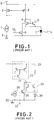
- Fig. 1 shows a laser drive circuit categorized as a cathode-common type circuit as known in the prior art.
- a component 1 is a base current source for determining the drive current to the laser semiconductor, which is ordinarily controlled so that the output voltage which is the quantity of laser light may be regulated to be a designated value by monitoring the quantity of laser light from the laser light-emitting device by means of a photo-diode not shown.
- Components 2 and 3 form a current mirror circuit composed of a couple of P-channel MOS transistors, where both of the drain and source terminals of the PMOS transistor 2 are connected to the base current source 1. The value of the drain current to the PMOS transistor 2 is reflected (mirrored) to the value of the output current from the PMOS transistor 3.
- the drain terminal of the PMOS transistor 3 is connected to the terminal shorted both to the collector and base of the NPN transistor 4.
- the base of the NPN transistor 5 is connected to the terminal shorted both to the collector and base of the NPN transistor 4. With these NPN transistors 4 and 5, a current mirror circuit is formed.
- the ratio of the area of the emitter of the NPN transistor 4 to the area of the emitter of the NPN transistor 5 is 1:N, the value of the output current from the emitter terminal common to the transistors 4 and 5 may be obtained so as to be (1+N) times as large as the value of the drain current to the PMOS transistor 3.
- a component 7 is a laser diode, and its cathode is connected to the ground level point (GND) 9, while its anode is connected the common-emitter terminal of the NPN transistors 4 and 5.
- the N-Channel MOS transistor 6 is a switching transistor which is turned on when the high-level signal is applied to the control signal input terminal, and to which the current supplied from the PMOS transistor 3 is led. In this state, a current is not supplied to the short-circuit terminal to the collector and base of the NPN transistor 4, and thus the current mirror circuit formed by the NPN transistors 4 and 5 is turned off. Therefore, the drive current for the laser diode 7 is zero.
- the output current from the PMOS transistor 3 drives the laser diode 7 by driving the current mirror circuit composed of the NPN transistors 4 and 5. And then, the light emission from the laser diode 7 is switched in a high speed by turning the NMOS transistor 6 on and off in a high speed.
- Fig. 2 shows another example of the semiconductor laser drive circuit as known in the prior art.
- the cathode of the laser diode 30 is connected to the lower electric potential terminal 22 in the circuit, and its anode is connected to the current mirror circuit 24.
- the input terminal to the current mirror circuit 24 is connected to the output terminal from the constant-current circuit 23.
- the emitter of the NPN transistor 25 which is switched by the control signal supplied from outside the circuit is connected to the lower electric potential terminal 22, and its base is connected to the control signal input terminal 12 and its collector is connected to the output terminal from the constant-current circuit 23.
- the semiconductor laser diode 30 emits laser light in responsive to the current supplied to itself. Its light emission process is stated as below. At first, when the voltage applied to the control signal input terminal 32 is V H , the NPN transistor 25 is turned on and the current supplied by the constant-current source 23 is led to the NPN transistor 25 and is not supplied to the current mirror circuit 24 and hence as the current is not also supplied to the laser diode 30, and the laser light is not emitted.
- the NPN transistor 25 is turned off and the current supplied by the constant-current source 23 is led to the current mirror circuit 24 and hence, as the current is also supplied to the laser diode 30, and the laser light is emitted from the laser diode 30.
- the electric potential at the base of the current mirror circuit 24 is the sum of the voltage V F defined between the anode and the cathode of the laser diode 30 and the voltage V BE(ON) defined between the emitter and the base of the current mirror circuit 24.
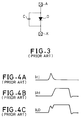
- Fig. 3 shows an equivalent circuit of the laser diode 7.
- A is the anode terminal
- K is the cathode terminal
- D is the junction part of the laser diode
- C is the junction capacitance of the laser diode.
- the laser drive circuit shown in Fig. 9 drives the laser diode 7
- the current is led to the laser diode junction part D when the voltage V F defined between the terminals of the laser diode rises up to about 1 to 1.5V.
- the drive current in the laser drive circuit is at first used for charging the junction capacitance C, and when V F rises up to the voltage with which the laser light can be emitted from the laser diode, the fraction of the current used for charging the junction capacitance C is reduced and the effective current is led to the junction part D of the laser diode.
- Figs. 4A-4C show waveforms of currents supplied into the laser diode shown in Figs. 1 and 2.
- the waveform (Fig. 4A) in Fig. 4 refers to the current Icj led to the junction capacitance C
- the waveform (Fig. 4B) refers to the current Ild led to the laser diode junction part D
- the waveform (Fig. 4C) refers to the current ILD led to the anode terminal A.
- the current ILD led to the anode terminal A is the sum of Icj and Ild, and hence, the peak of the waveform of the current Icj used for charging the junction part D makes a noise onto the current ILD led to the anode terminal A.
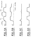
- Figs. 5A-5D show waveforms of currents and voltage with the turn-off time period of the laser diode shown in Figs. 1 and 2 changed.
- the waveform (Fig. 5A) refers to the laser drive current ILD led to the anode terminal A of the laser diode 7
- the waveform (Fig. 5B) refers to the voltage V F
- the waveform (Fig. 5C) refers to the charge current Icj for charging the laser diode junction capacitance C
- the waveform (Fig. 5D) refers to the current Ild led to the junction part D of the laser diode.
- the pulse P1 in the waveform in Fig. 5A is a step response of the laser drive current when the laser diode is driven after a long time Toffl during which the laser diode has been turned off. That is, Toff1 is far grater than Toff2.
- Toff1 is far grater than Toff2.
- the waveform in Fig. 5B while the time period Toffl in which the laser diode is turned off in a long time, the electric charge stored in the laser diode junction capacitance C is almost discharged with a small quantity of Off current, and hence, V F goes down to the GND level. Therefore, the additional current is required for charging the laser diode junction capacitance C when the laser diode is turned on next, and the charge current flows in the waveform in Fig. 5C.
- the current led to the anode terminal A takes a step response shaped in the pulse P1 containing a noise in its rise-up part.
- the pulse P2 formed after a short period Toff2 after the fall-down of the pulse P1 As the laser diode is turned on before the electric charge stored in the laser diode junction capacitance C is not fully discharged, the voltage V F does not fall down to the GND level at the beginning of the pulse P2 as shown in the waveform in Fig. 5B, and the charge current shown by Fig. 5C flows a little. Therefore, the current ILD led to the anode terminal A does not contain noises. In addition, as the pulse P2 does not need the current Icj, the rise-up speed of the pulse P2 is faster than the pulse P1.
- the laser diode 30 Due to the time constant developed in the time domain behavior for charging the above described capacitances, the laser diode 30 emits laser light with a delayed time after the voltage applied to the control input terminal 32 changes from V H to V L . Especially, in case of reducing the output current from the constant-current circuit 23 in order to reduce the output power of laser light, the delayed time for emitting laser light is remarkable and can not be ignored for attaining the high-speed switching response of the laser light.
- An object of the present invention is to provide a drive circuit enabling a high-speed switching response in semiconductor light emitting devices and removing noises from its drive current.
- a driver integrated circuit comprises: means for generating a drive current; means for switching an output of the drive current to an output terminal; and means for generating a bias current, in which the bias current generated by the bias current generating means is supplied to the output terminal independent on a state of the switching means.
- the bias-current generating means may comprise a resistor.
- the bias current generating means may comprise current mirror transistors.
- the driver integrated circuit may drive a semiconductor light emitting element.
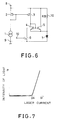
- Fig. 6 shows the first embodiment of the present invention.
- This circuit is a driver IC for driving a laser diode 7.
- a component 1 is a base current source for defining the drive current of laser
- components 2 and 3 are defined as a current mirror circuit formed by PMOS transistors
- components 4 and 5 are defined as a current mirror circuit formed by NPN transistors.
- a component 6 is an N-channel MOS transistor for switching a drive current.
- An input terminal for ON/OFF switching control signals is connected to the gate of the NMOS transistor 6.
- a terminal 8 is for accepting the power supply Vcc, and numeral 9 indicates a ground point (GND).
- GND ground point
- the laser diode drive current is put out from the common terminal to emitters of NPN transistors 4 and 5, and is supplied to the anode terminal of the laser diode 7.
- the cathode terminal of the laser diode 7 is connected to the GND 9.
- the resistance 10 for defining a bias current which is specific to this driver IC, is connected to the anode terminal of the laser diode 7.
- the other terminal of the resistance 10 for defining a bias current is connected to the power supply Vcc 8.
- a bias current defined by the following equation is supplied through the resistance 10 for defining a bias current to the anode terminal of the laser diode 7 when the laser is turned off.
- Ibias Vcc - V F(OFF) R B where V F(OFF) is V F of the laser diode when it is turned off, and
- R B is the value of the resistance for defining a bias current.
- Ibias its value is determined so that the laser diode may not emit lights.
- Fig. 7 shows a relationship between the intensity of light emitted from the laser diode and the drive current. As shown in Fig. 7, in the range where the laser current IF is less than the threshold current Ith, the laser output power P is extremely small, and, in the range where the laser current IF gets over IF, the laser output power P increases extremely as the laser current IF increases.
- Figs. 8A-8D show waveforms observed when Ibias is supplied to the laser diode 7.
- Fig. 8A shows the current ILD running into the anode terminal.
- Toff1 the turn-off time of the laser before the pulse P1 is turned on
- Toff2 the turn-off time of the laser before the pulse P2 is turned on
- the voltage V F developed at the laser diode 7 does not fall down to the GND level as shown in Fig. 8B. This is because the junction capacitance is charged by Ibias, and thus a designated quantity of electric charge is not lost in the laser diode 7. Therefore, the charge current Icj flowing through the junction part of the laser diode does not change even if Toff changes, but is kept to be an extremely small value independently upon Toff as shown in Fig. 8C.
- the current ILD to the anode terminal is defined to be the sum of the charge current Icj and the laser diode junction part current Ild as shown in Fig. 8D, it can be avoided that spike noises occur simultaneously at the rise-up part of the current waveform, and the degradation of the rise-up time can be reduced.
- Fig. 9 shows the second embodiment of the present invention.
- This embodiment is a driver IC like the first embodiment, but the laser current is supplied by a current mirror circuit in stead of the resistance 10 for defining the bias current of the first embodiment shown in Fig. 6.
- the collector of the PNP transistor 10 is connected to the anode terminal of the laser diode 7
- the base of the PNP transistor 10 is connected to the collector-base short terminal of the PNP transistor 11.
- the emitters of the PNP transistors 10 and 11 are connected to the power supply Vcc 8, and furthermore, the base of the PNP transistor and the collector-base short terminal of the PNP transistor 11 are connected to the constant-current source 12.
- the ratio of the area of the emitter of the PNP transistor 10 to the area of the emitter of the PNP transistor 11 is 1, the value of the current from the constant-current source 12 is reflected to the current supplied from the collector of the PNP transistor 10 to the anode terminal of the laser diode 7.
- This current is established as a bias current for charging the junction capacitor of the laser diode.
- the bias current is generated within the driver IC, the number of devices outside of the driver IC can be reduced.
- Fig. 10 shows the third embodiment of the present invention. Following embodiments are preferably structured by IC.
- a component 21 is a power supply line
- a component 22 is a ground line
- a component 23 is a constant-current circuit
- a component 24 is a current mirror circuit
- a component 25 is an NPN transistor for switching
- a component 26 is a current source
- a component 27 is a level shift circuit using diodes
- a component 28 is a BicMOS inverter
- a component 29 is an inverter
- a component 30 is a semiconductor laser diode
- a component 32 is an input terminal for control signals.
- the output from the inverter 28 is lower voltage, and therefore, the output from the inverter 29 is high voltage designated V OH .
- the NPN transistor 25 is turned on and the current supplied by the constant-current source 23 is led to the NPN transistor 25 and is not supplied to the current mirror circuit 24, and therefore, as the current is not supplied to the laser diode 30, the laser light is not emitted.
- the diode is in a zero-biased state and the current does not flow in the diode.
- the output from the inverter 29 is lower voltage, and therefore, the output from the inverter 25 is high voltage. Therefore, in order to turn off the NPN transistor 25 for switching from its turn-on state, the output current supplied by the constant-current circuit 23 begins to be supplied to the current mirror circuit 24, and at the same time, as the output from the inverter 28 is high voltage, this voltage is transferred through the level shift circuit 27 to the electric potential of the base of the current mirror circuit 24, and thus the base potential is suddenly raised.
- the above base potential has the value V CH - n V DF which is subtracted the value n V DF from the output of the inverter 28, in which n V DF is obtained by multiplying the number (n) of the diodes serially connected in the level shift circuit 27 to the forward potential (V DF ) of the diode.
- V CH - n V DF has somewhat lower than the value V BE(ON) + V F in the prior art(see Fig. 2)
- the value of n or the junction area of the diode must be adjusted.
- the above time is very short. Accordingly, it becomes possible to switch at a high speed the laser light emission.
- the output potential of the level shift circuit is smaller than the value V BE(ON) + V F as described above. Therefore, since the diodes in the level shift circuit is at a zero-biased state or reverse-biased state when the output current of the constant current circuit 23 flows into the current mirror circuit 24 and the desired current is supplied to the laser diode 30, the current does not flow into the laser diode 30, it never effect on the setting of the driving current to the laser diode 30 by the current source 26.
- Figs. 11 and 12 are embodiments which modified the embodiment shown in Fig. 10. Namely, it may be possible to use an n-stage of emitter follower as shown in Fig. 11 or an n-stage of a source follower as shown in Fig. 12.
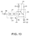
- the fifth embodiment shown in Fig. 13 is fundamentally the same as one in Fig. 10, except that an ordinary inverter is used as the inverter 28 in this embodiment. Namely, any ordinary drivers which has a lower output impedance may be used as the inverter 28.
- Fig. 14 shows another embodiment of the present invention.
- a cathode of a laser diode 30 is connected to a lower potential point 22 in a circuit, an anode of the diode is connected to a current mirror circuit 24 of which an input is connected to an output of a constant current circuit 23.
- the lower electric potential point 22 is connected to an emitter of an NPN transistor 25 which can be switched by a control signal, a base of the NPN transistor 25 is an output of a level shift circuit 27 of which an input is connected to an output of a voltage driver.
- an output of an inverter 28 is at a high potential when a control input terminal is at a lower potential V L . Therefore, an output of an inverter 29 and the output of the level shift circuit 27 are turned into a lower potential. As a result, the switching transistor 25 is turned on to draw an output current of the constant current source 23. Accordingly, since any current can not be supplied into the laser diode 30, it does not emit light.
- This embodiment also has the same effects as that in the embodiment described above.
- the inverter 29 and the level shift circuit 27 a certain time td to obtain the maximum value of the output current of the level shift circuit 27 from when the control input terminal 32 changes from the low potential to the high potential and the switching transistor 25 switches from the turned-on state to the turned-off state. Accordingly, if the laser driver is driven at a higher frequency, it may be necessary to take account of the time td.
- Fig. 15 shows the seventh embodiment of the present invention in which like elements corresponding to those of the above embodiment are identified by the same reference numerals, and the explanation of the like elements will be abbreviated.
- a delay element 39 is inserted between an input of an NPN switching transistor and the control input terminal.
- an input waveform of the level shift circuit 27 changes to the high potential after the delay time of the inverter 29 elapses.
- the base of the switching transistor changes to the low potential after the delay time of the delay element 39, its collector current decrease along with change in the base current.
- the output of the level shift circuit 27 is already at the high potential, the current is supplied at a high speed from the output of the level shift circuit 27 to the input of the current mirror circuit 24, and thus the base potential of the current mirror circuit 24 is also raised at a high speed.
- the level shift circuit 27 become apart from a forward bias, and thus it does not supply the output current. Therefore, the current supplied to the input of the current mirror circuit 24 is only the output current of the constant current source 23, in which the laser diode 30 is driven by the constant current with the set value.
- the present invention since a bias current is always flowed to an anode terminal of the semiconductor light emitting element, it is possible to precharge a junction capacity of the semiconductor light emitting element, and thus it is possible to eliminate the charge current of the junction capacitance without regard to the length of the turned-off time of semiconductor light emitting device. As a result, spike noises in the rising part and the deterioration of the rising speed of the waveform which depend on the turned-off time of a semiconductor light emitting device, are suppressed.
- the semiconductor light emitting device Since it can charge at a high speed a parasitic capacitance accompanying such as a semiconductor emitting element and a current mirror circuit for driving it just before the turned-on state of the current mirror circuit, by using the voltage driver and the level regulating means, it is possible to allow the semiconductor light emitting device to emit the light and stop emitting it at a high speed without effecting on the setting of the current flowing to the semiconductor light emitting device.
- a drive circuit for supplying a constant drive current to the anode terminal of a semiconductor light emitting device includes a current supply source connected to the anode terminal for supplying a bias current to the semiconductor light emitting device. Since the drive circuit is formed so as to supply the bias current to the anode terminal of the semiconductor light emitting device, a charge current for charging a conjunction capacitance can be reduced independently on the time period of turning off the semiconductor light emitting device. As a result, a spike noise can be removed in the laser current waveform at its rise-up part, and a reduction of its rise-up speed can be restricted, both of which are due to a dependent upon the time period of turning off the semiconductor device.
Landscapes
- Physics & Mathematics (AREA)
- Condensed Matter Physics & Semiconductors (AREA)
- General Physics & Mathematics (AREA)
- Electromagnetism (AREA)
- Optics & Photonics (AREA)
- Semiconductor Lasers (AREA)
- Led Devices (AREA)
- Control Of Amplification And Gain Control (AREA)
Abstract
Description
- The present invention relates to a drive circuit for semiconductor light-emitting device. More specifically, this invention relates to a drive circuit for semiconductor light-emitting device which is applicable to a laser drive integrated circuit (IC) for high-speed switching used for, for example, magneto-optical disks and laser beam printers.
- Fig. 1 shows a laser drive circuit categorized as a cathode-common type circuit as known in the prior art. In Fig. 1, a
component 1 is a base current source for determining the drive current to the laser semiconductor, which is ordinarily controlled so that the output voltage which is the quantity of laser light may be regulated to be a designated value by monitoring the quantity of laser light from the laser light-emitting device by means of a photo-diode not shown.Components 2 and 3 form a current mirror circuit composed of a couple of P-channel MOS transistors, where both of the drain and source terminals of thePMOS transistor 2 are connected to the basecurrent source 1. The value of the drain current to thePMOS transistor 2 is reflected (mirrored) to the value of the output current from the PMOS transistor 3. - The drain terminal of the PMOS transistor 3 is connected to the terminal shorted both to the collector and base of the NPN transistor 4. The base of the
NPN transistor 5 is connected to the terminal shorted both to the collector and base of the NPN transistor 4. With theseNPN transistors 4 and 5, a current mirror circuit is formed. By making the ratio of the area of the emitter of the NPN transistor 4 to the area of the emitter of theNPN transistor 5 is 1:N, the value of the output current from the emitter terminal common to thetransistors 4 and 5 may be obtained so as to be (1+N) times as large as the value of the drain current to the PMOS transistor 3. - A
component 7 is a laser diode, and its cathode is connected to the ground level point (GND) 9, while its anode is connected the common-emitter terminal of theNPN transistors 4 and 5. The N-Channel MOS transistor 6 is a switching transistor which is turned on when the high-level signal is applied to the control signal input terminal, and to which the current supplied from the PMOS transistor 3 is led. In this state, a current is not supplied to the short-circuit terminal to the collector and base of the NPN transistor 4, and thus the current mirror circuit formed by theNPN transistors 4 and 5 is turned off. Therefore, the drive current for thelaser diode 7 is zero. In addition, as theNMOS transistor 6 is turned off when the low-level signal is applied to theinput terminal 10, the output current from the PMOS transistor 3 drives thelaser diode 7 by driving the current mirror circuit composed of theNPN transistors 4 and 5. And then, the light emission from thelaser diode 7 is switched in a high speed by turning theNMOS transistor 6 on and off in a high speed. - Fig. 2 shows another example of the semiconductor laser drive circuit as known in the prior art. In Fig. 2, the cathode of the
laser diode 30 is connected to the lower electricpotential terminal 22 in the circuit, and its anode is connected to thecurrent mirror circuit 24. The input terminal to thecurrent mirror circuit 24 is connected to the output terminal from the constant-current circuit 23. The emitter of theNPN transistor 25 which is switched by the control signal supplied from outside the circuit is connected to the lowerelectric potential terminal 22, and its base is connected to the controlsignal input terminal 12 and its collector is connected to the output terminal from the constant-current circuit 23. - In the circuit shown in Fig. 2, the
semiconductor laser diode 30 emits laser light in responsive to the current supplied to itself. Its light emission process is stated as below. At first, when the voltage applied to the controlsignal input terminal 32 is VH, theNPN transistor 25 is turned on and the current supplied by the constant-current source 23 is led to theNPN transistor 25 and is not supplied to thecurrent mirror circuit 24 and hence as the current is not also supplied to thelaser diode 30, and the laser light is not emitted. - Next, when the voltage applied to the
control signal input 32 is VL, theNPN transistor 25 is turned off and the current supplied by the constant-current source 23 is led to thecurrent mirror circuit 24 and hence, as the current is also supplied to thelaser diode 30, and the laser light is emitted from thelaser diode 30. At this time, the electric potential at the base of thecurrent mirror circuit 24 is the sum of the voltage VF defined between the anode and the cathode of thelaser diode 30 and the voltage VBE(ON) defined between the emitter and the base of thecurrent mirror circuit 24. - However, in the prior art shown in Fig. 9, as the charge current for charging the junction capacitance in the laser diode, the following disadvantages are found.
- (1) When the laser diode is turned on after a long period of time while which the laser diode is turned off, spike noises occur at the rise-up part of the waveform of the current supplied to the anode terminal of the laser diode.
- (2)The rise-up speed of the current when the laser diode is turned on after a longer period of time while which the laser diode is turned off is slower than the rise-up speed of the current when the laser diode is turned on after a shorter period of time while which the laser diode is turned off.
- The factors leading to the above disadvantages (1) and (2) are described below.
- Fig. 3 shows an equivalent circuit of the
laser diode 7. In Fig. 3, A is the anode terminal, K is the cathode terminal, D is the junction part of the laser diode, and C is the junction capacitance of the laser diode. In case that the laser drive circuit shown in Fig. 9 drives thelaser diode 7, the current is led to the laser diode junction part D when the voltage VF defined between the terminals of the laser diode rises up to about 1 to 1.5V. That is, the drive current in the laser drive circuit is at first used for charging the junction capacitance C, and when VF rises up to the voltage with which the laser light can be emitted from the laser diode, the fraction of the current used for charging the junction capacitance C is reduced and the effective current is led to the junction part D of the laser diode. - Figs. 4A-4C show waveforms of currents supplied into the laser diode shown in Figs. 1 and 2. The waveform (Fig. 4A) in Fig. 4 refers to the current Icj led to the junction capacitance C, the waveform (Fig. 4B) refers to the current Ild led to the laser diode junction part D, and the waveform (Fig. 4C) refers to the current ILD led to the anode terminal A. In the time domain, the current ILD led to the anode terminal A is the sum of Icj and Ild, and hence, the peak of the waveform of the current Icj used for charging the junction part D makes a noise onto the current ILD led to the anode terminal A.
- Next, the factor leading to the above disadvantage (2) is described below.
- Figs. 5A-5D show waveforms of currents and voltage with the turn-off time period of the laser diode shown in Figs. 1 and 2 changed. In this figure, the waveform (Fig. 5A) refers to the laser drive current ILD led to the anode terminal A of the
laser diode 7, the waveform (Fig. 5B) refers to the voltage VF, the waveform (Fig. 5C) refers to the charge current Icj for charging the laser diode junction capacitance C, and the waveform (Fig. 5D) refers to the current Ild led to the junction part D of the laser diode. - Individual waveforms show differences in the time-domain behavior in responsive to the change of the turn-off time period of the drive current of the laser diode.
- The pulse P1 in the waveform in Fig. 5A is a step response of the laser drive current when the laser diode is driven after a long time Toffl during which the laser diode has been turned off. That is, Toff1 is far grater than Toff2. As shown in the waveform in Fig. 5B, while the time period Toffl in which the laser diode is turned off in a long time, the electric charge stored in the laser diode junction capacitance C is almost discharged with a small quantity of Off current, and hence, VF goes down to the GND level. Therefore, the additional current is required for charging the laser diode junction capacitance C when the laser diode is turned on next, and the charge current flows in the waveform in Fig. 5C. Eventually, the current led to the anode terminal A takes a step response shaped in the pulse P1 containing a noise in its rise-up part.
- As for the pulse P2 formed after a short period Toff2 after the fall-down of the pulse P1, as the laser diode is turned on before the electric charge stored in the laser diode junction capacitance C is not fully discharged, the voltage VF does not fall down to the GND level at the beginning of the pulse P2 as shown in the waveform in Fig. 5B, and the charge current shown by Fig. 5C flows a little. Therefore, the current ILD led to the anode terminal A does not contain noises. In addition, as the pulse P2 does not need the current Icj, the rise-up speed of the pulse P2 is faster than the pulse P1.
- In summing up, in the laser drive circuit in the prior art shown in Fig. 1, after a long period of time while the laser diode is turned off, a spike noise is contained in the laser current waveform at its rise-up part, and its rise-up speed is restricted.
- These disadvantages described above are found in another prior art shown in Fig. 2. Parasitic capacitors are formed at the output terminal of the constant-
current circuit 23, the collector of the switchingNPN transistor 25, and the collector and base of thecurrent mirror circuit 24, and individual parasitic capacitors are charged by the output current from the constant-current circuit 23 when the switchingNPN transistor 25 is transferred from the turn-off state to the turn-on state. And then, a designated quantity of current is led to thecurrent mirror circuit 24 when the electric potential at the base of thecurrent mirror circuit 24 rises up from VCE(SAT) to VF + VBE(ON), and finally, thelaser diode 30 emits laser light with its intensity determined in responsive to the current led to the laser diode. - Due to the time constant developed in the time domain behavior for charging the above described capacitances, the
laser diode 30 emits laser light with a delayed time after the voltage applied to thecontrol input terminal 32 changes from VH to VL. Especially, in case of reducing the output current from the constant-current circuit 23 in order to reduce the output power of laser light, the delayed time for emitting laser light is remarkable and can not be ignored for attaining the high-speed switching response of the laser light. - An object of the present invention is to provide a drive circuit enabling a high-speed switching response in semiconductor light emitting devices and removing noises from its drive current.
- According to the present invention, a driver integrated circuit comprises:
means for generating a drive current;
means for switching an output of the drive current to an output terminal; and
means for generating a bias current,
in which the bias current generated by the bias current generating means is supplied to the output terminal independent on a state of the switching means. - Here, the bias-current generating means may comprise a resistor.
- The bias current generating means may comprise current mirror transistors.
- The driver integrated circuit may drive a semiconductor light emitting element.
- The above and other objects, effects, features and advantages of the present invention will become more apparent from the following description of embodiments thereof taken in conjunction with the accompanying drawings.
- Fig. 1 is a circuit diagram showing a prior art drive circuit for laser diodes of a cathode common type;
- Fig. 2 is a circuit diagram showing another embodiment;
- Fig. 3 is an equivalent circuit of the laser diode;
- Figs. 4A-4C are waveforms showing currents supplied into the laser diode shown in Figs. 1 and 2;
- Figs. 5A-5D are waveforms showing currents supplied into the laser diode shown in Figs. 9 and 10;
- Fig. 6 is a circuit diagram showing the first embodiment of the present invention;
- Fig. 7 is a characteristic curve showing a relationship between the intensity of light from a laser diode and a drive current of the laser diode;
- Figs. 8A-8D are waveforms showing currents supplied into the
laser diode 7 shown in Fig. 6; - Fig. 9 is a circuit diagram showing the second embodiment of the present invention;
- Fig. 10 is a circuit diagram showing the third embodiment of the present invention;
- Fig. 11 is a diagrammatical picture showing a multi-stage emitter follower circuit using NPN transistors as another embodiment of the
level shift circuit 27 shown in Fig. 10; - Fig. 12 is a diagrammatical picture showing a multi-stage emitter follower circuit using NMOS transistors as another embodiment of the
level shift circuit 27 shown in Fig. 10; - Fig. 13 is a circuit diagram showing a modification of the embodiment shown in Fig. 10;
- Fig. 14 is a circuit diagram showing the sixth embodiment of the present invention;
- Fig. 15 is a circuit diagram showing the seventh embodiment of the present invention; and
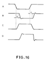
- Fig. 16 is a waveform showing voltages and currents measured at each node in the seventh embodiment.
- Fig. 6 shows the first embodiment of the present invention. This circuit is a driver IC for driving a
laser diode 7. In Fig. 6, acomponent 1 is a base current source for defining the drive current of laser,components 2 and 3 are defined as a current mirror circuit formed by PMOS transistors, andcomponents 4 and 5 are defined as a current mirror circuit formed by NPN transistors. Acomponent 6 is an N-channel MOS transistor for switching a drive current. An input terminal for ON/OFF switching control signals is connected to the gate of theNMOS transistor 6. Aterminal 8 is for accepting the power supply Vcc, and numeral 9 indicates a ground point (GND). As the principles of operations by each of components designatednumerals 1 to 6,8 and 9 are similar to the prior art described in Fig. 1, these are not repetitively described here. - The laser diode drive current is put out from the common terminal to emitters of
NPN transistors 4 and 5, and is supplied to the anode terminal of thelaser diode 7. The cathode terminal of thelaser diode 7 is connected to theGND 9. Theresistance 10 for defining a bias current, which is specific to this driver IC, is connected to the anode terminal of thelaser diode 7. The other terminal of theresistance 10 for defining a bias current is connected to thepower supply Vcc 8. - A bias current defined by the following equation is supplied through the
resistance 10 for defining a bias current to the anode terminal of thelaser diode 7 when the laser is turned off.
where VF(OFF) is VF of the laser diode when it is turned off, and - RB is the value of the resistance for defining a bias current.
- As for Ibias, its value is determined so that the laser diode may not emit lights.
- Fig. 7 shows a relationship between the intensity of light emitted from the laser diode and the drive current. As shown in Fig. 7, in the range where the laser current IF is less than the threshold current Ith, the laser output power P is extremely small, and, in the range where the laser current IF gets over IF, the laser output power P increases extremely as the laser current IF increases.
- By charging the junction capacitance into the laser diode while the laser is turned off with Ibias being adjusted so as to be less than Ith, which means that Ibias is so selected that the apparatus within which the laser diode is installed may not be given bad influences, and by regulating the charge current, when the laser diode is turned on from its turned-off state, in such a small value as it does not depend upon the turn off time of the laser, it will be appreciated that spike noises can be removed and that the degradation of the rise-up time can be reduced.
- Figs. 8A-8D show waveforms observed when Ibias is supplied to the
laser diode 7. Fig. 8A shows the current ILD running into the anode terminal. Suppose that the turn-off time of the laser before the pulse P1 is turned on is Toff1, and that the turn-off time of the laser before the pulse P2 is turned on is Toff2, then the relationship, Toff1>>Toff2, is established. - Even in the time period, Toffl, while the laser is turned off in a relatively long time, the voltage VF developed at the
laser diode 7 does not fall down to the GND level as shown in Fig. 8B. This is because the junction capacitance is charged by Ibias, and thus a designated quantity of electric charge is not lost in thelaser diode 7. Therefore, the charge current Icj flowing through the junction part of the laser diode does not change even if Toff changes, but is kept to be an extremely small value independently upon Toff as shown in Fig. 8C. Thus, as the current ILD to the anode terminal is defined to be the sum of the charge current Icj and the laser diode junction part current Ild as shown in Fig. 8D, it can be avoided that spike noises occur simultaneously at the rise-up part of the current waveform, and the degradation of the rise-up time can be reduced. - Fig. 9 shows the second embodiment of the present invention. This embodiment is a driver IC like the first embodiment, but the laser current is supplied by a current mirror circuit in stead of the
resistance 10 for defining the bias current of the first embodiment shown in Fig. 6. In Fig. 7, the collector of thePNP transistor 10 is connected to the anode terminal of thelaser diode 7, and the base of thePNP transistor 10 is connected to the collector-base short terminal of the PNP transistor 11. The emitters of thePNP transistors 10 and 11 are connected to thepower supply Vcc 8, and furthermore, the base of the PNP transistor and the collector-base short terminal of the PNP transistor 11 are connected to the constant-current source 12. - Therefore, if the ratio of the area of the emitter of the
PNP transistor 10 to the area of the emitter of the PNP transistor 11 is 1, the value of the current from the constant-current source 12 is reflected to the current supplied from the collector of thePNP transistor 10 to the anode terminal of thelaser diode 7. This current is established as a bias current for charging the junction capacitor of the laser diode. As a result, as explained above with Fig. 8, it can be avoided that spike noises occur simultaneously at the rise-up part of the current waveform, and the degradation of the rise-up time can be reduced, both of which are caused by the change of the turn-off time period of the laser diode. - As the bias current is generated within the driver IC, the number of devices outside of the driver IC can be reduced.
- Fig. 10 shows the third embodiment of the present invention. Following embodiments are preferably structured by IC. In Fig. 10, a
component 21 is a power supply line, acomponent 22 is a ground line, acomponent 23 is a constant-current circuit, acomponent 24 is a current mirror circuit, acomponent 25 is an NPN transistor for switching, acomponent 26 is a current source, acomponent 27 is a level shift circuit using diodes, acomponent 28 is a BicMOS inverter, acomponent 29 is an inverter, acomponent 30 is a semiconductor laser diode, and acomponent 32 is an input terminal for control signals. - Next, what is described is an operation of the circuit in the third embodiment.
- When the voltage applied to the control
signal input terminal 32 is VH, the output from theinverter 28 is lower voltage, and therefore, the output from theinverter 29 is high voltage designated VOH. TheNPN transistor 25 is turned on and the current supplied by the constant-current source 23 is led to theNPN transistor 25 and is not supplied to thecurrent mirror circuit 24, and therefore, as the current is not supplied to thelaser diode 30, the laser light is not emitted. - At this time, as the difference of electric potentials between both end terminals of the
level shift circuit 27 is not found, the diode is in a zero-biased state and the current does not flow in the diode. - Next, in case that the voltage applied to the control
signal input terminal 32 is VL, the output from theinverter 29 is lower voltage, and therefore, the output from theinverter 25 is high voltage. Therefore, in order to turn off theNPN transistor 25 for switching from its turn-on state, the output current supplied by the constant-current circuit 23 begins to be supplied to thecurrent mirror circuit 24, and at the same time, as the output from theinverter 28 is high voltage, this voltage is transferred through thelevel shift circuit 27 to the electric potential of the base of thecurrent mirror circuit 24, and thus the base potential is suddenly raised. - The above base potential has the value VCH - nVDF which is subtracted the value nVDF from the output of the
inverter 28, in which nVDF is obtained by multiplying the number (n) of the diodes serially connected in thelevel shift circuit 27 to the forward potential (VDF) of the diode. In order that the value VCH - nVDF has somewhat lower than the value VBE(ON) + VF in the prior art(see Fig. 2), the value of n or the junction area of the diode must be adjusted. As compared with the time necessary for charging the parasitic capacity by using the output current of the constantcurrent circuit 23 of the prior art shown in Fig. 2 and then causing the base potential of thecurrent mirror circuit 24 to be the value VBE(ON) + VF, in the present embodiment, the above time is very short. Accordingly, it becomes possible to switch at a high speed the laser light emission. - When the control input terminal is at low potential, the output potential of the level shift circuit is smaller than the value VBE(ON) + VF as described above. Therefore, since the diodes in the level shift circuit is at a zero-biased state or reverse-biased state when the output current of the constant
current circuit 23 flows into thecurrent mirror circuit 24 and the desired current is supplied to thelaser diode 30, the current does not flow into thelaser diode 30, it never effect on the setting of the driving current to thelaser diode 30 by thecurrent source 26. - Figs. 11 and 12 are embodiments which modified the embodiment shown in Fig. 10. Namely, it may be possible to use an n-stage of emitter follower as shown in Fig. 11 or an n-stage of a source follower as shown in Fig. 12.
- The fifth embodiment shown in Fig. 13 is fundamentally the same as one in Fig. 10, except that an ordinary inverter is used as the
inverter 28 in this embodiment. Namely, any ordinary drivers which has a lower output impedance may be used as theinverter 28. - In the embodiment shown in Fig. 13, the
current source 26 shown in Fig. 10 is removed and the current source is directly connected as the constantcurrent circuit 23. - Fig. 14 shows another embodiment of the present invention. In Fig. 14, a cathode of a
laser diode 30 is connected to a lowerpotential point 22 in a circuit, an anode of the diode is connected to acurrent mirror circuit 24 of which an input is connected to an output of a constantcurrent circuit 23. The lower electricpotential point 22 is connected to an emitter of anNPN transistor 25 which can be switched by a control signal, a base of theNPN transistor 25 is an output of alevel shift circuit 27 of which an input is connected to an output of a voltage driver. - In operation, an output of an
inverter 28 is at a high potential when a control input terminal is at a lower potential VL. Therefore, an output of aninverter 29 and the output of thelevel shift circuit 27 are turned into a lower potential. As a result, the switchingtransistor 25 is turned on to draw an output current of the constantcurrent source 23. Accordingly, since any current can not be supplied into thelaser diode 30, it does not emit light. - Next, when a
control input terminal 32 is turned into the high potential VH, the output of theinverter 28 is turned into the lower potential. As a result, the switchingtransistor 25 switched from its turned-on state to its turned-off state, so that the output current of the constantcurrent source 23 begins to flow into thecurrent mirror circuit 24. The output of theinverter 29 becomes at the high potential just after the current flowing. Thus thelevel shift circuit 27 becomes at a conductive state and the output current of one is supplied to thecurrent mirror circuit 24. As a result, a base potential of thecurrent mirror circuit 24 is suddenly raised, and then thecurrent mirror circuit 24 gradually supplies a current to thelaser diode 30. When the magnitude of the supplied current become larger than a predetermined threshold value, the laser diode begins to emit the light. - This embodiment also has the same effects as that in the embodiment described above.
- However, it takes the
inverter 29 and the level shift circuit 27 a certain time td to obtain the maximum value of the output current of thelevel shift circuit 27 from when thecontrol input terminal 32 changes from the low potential to the high potential and the switchingtransistor 25 switches from the turned-on state to the turned-off state. Accordingly, if the laser driver is driven at a higher frequency, it may be necessary to take account of the time td. - Next, another embodiment of the present invention will be explained, in which a delay element is inserted between an input terminal of the voltage driver switched by the control input and an input terminal of an active element switched by the control input, the effect of an operation delay time of the voltage driver and the level regulation means is eliminated by operating the voltage driver before the active element is switched, it is, therefore, possible to minimize the time from when the active element is switched from the turned-on state to the turned-off state to when the
current mirror circuit 24 begins to supply a current to the laser diode. - Fig. 15 shows the seventh embodiment of the present invention in which like elements corresponding to those of the above embodiment are identified by the same reference numerals, and the explanation of the like elements will be abbreviated.
- In this embodiment, a
delay element 39 is inserted between an input of an NPN switching transistor and the control input terminal. - In operation, when the
control input terminal 32 is at a high potential VH, an output of thedelay element 39 is also at a high potential. Thus the switchingtransistor 25 is at the turned-on state and the output current of the constantcurrent source 23 flows thereinto. At this time, since the output of theinverter 29 is at the low potential, thelevel shift circuit 27 does not provide the output current. Therefore, any current are not supplied to thecurrent mirror circuit 24 and thus thelaser diode 30, as result, the laser diode does not emit the light. Next, referring to Fig. 16, the operation when thecontrol input terminal 32 changes to the low potential will be explained. - In the figure, each symbols indicate as follows;
- A: a waveform of the control signal input terminal;
- B: a base waveform of the switching
transistor 25; - C: an input waveform of the
level shift circuit 27; - D: a cathode current of the
laser diode 30; and - d: delay time of the
inverter 29. - When the control input terminal changes from the high potential to the low potential, an input waveform of the
level shift circuit 27 changes to the high potential after the delay time of theinverter 29 elapses. The base of the switching transistor changes to the low potential after the delay time of thedelay element 39, its collector current decrease along with change in the base current. At this time, since the output of thelevel shift circuit 27 is already at the high potential, the current is supplied at a high speed from the output of thelevel shift circuit 27 to the input of thecurrent mirror circuit 24, and thus the base potential of thecurrent mirror circuit 24 is also raised at a high speed. When the base potential of thecurrent mirror circuit 24 rises just before the value which can supply a desired current to thelaser diode 30, thelevel shift circuit 27 become apart from a forward bias, and thus it does not supply the output current. Therefore, the current supplied to the input of thecurrent mirror circuit 24 is only the output current of the constantcurrent source 23, in which thelaser diode 30 is driven by the constant current with the set value. - By using such the
delay element 39, it is possible to decrease very much the time from when the switchingtransistor 25 switches from the turned-on state to the turned-off state to when the set current is supplied to thelaser diode 30, and it is also possible to drive it at a high speed. - As described hereinbefore, in the present invention, since a bias current is always flowed to an anode terminal of the semiconductor light emitting element, it is possible to precharge a junction capacity of the semiconductor light emitting element, and thus it is possible to eliminate the charge current of the junction capacitance without regard to the length of the turned-off time of semiconductor light emitting device. As a result, spike noises in the rising part and the deterioration of the rising speed of the waveform which depend on the turned-off time of a semiconductor light emitting device, are suppressed.
- Since it can charge at a high speed a parasitic capacitance accompanying such as a semiconductor emitting element and a current mirror circuit for driving it just before the turned-on state of the current mirror circuit, by using the voltage driver and the level regulating means, it is possible to allow the semiconductor light emitting device to emit the light and stop emitting it at a high speed without effecting on the setting of the current flowing to the semiconductor light emitting device.
- The invention may be embodied in other specific forms without departing from the spirit or essential characteristics thereof. The present embodiment is therefore to be considered in all respects as illustrative and not restrictive, the scope of the invention being indicated by the appended claims rather than by the foregoing description and all changes which come within the meaning and range of equivalency of the claims are therefore intended to be embraced therein.
- The present invention has been described in detail with respect to preferred embodiments, and it will now be apparent from the foregoing to those skilled in the art that changes and modifications may be made without departing from the invention in its broader aspects, and it is the intention, therefore, in the appended claims to cover all such changes and modifications as fall within the true spirit of the invention.
- A drive circuit for supplying a constant drive current to the anode terminal of a semiconductor light emitting device, includes a current supply source connected to the anode terminal for supplying a bias current to the semiconductor light emitting device. Since the drive circuit is formed so as to supply the bias current to the anode terminal of the semiconductor light emitting device, a charge current for charging a conjunction capacitance can be reduced independently on the time period of turning off the semiconductor light emitting device. As a result, a spike noise can be removed in the laser current waveform at its rise-up part, and a reduction of its rise-up speed can be restricted, both of which are due to a dependent upon the time period of turning off the semiconductor device.
Claims (4)
- An integrated drive circuit, comprising:a) means (1) for generating a drive current;b) means (6) for switching an output of the drive current to an output terminal; andc) means (10; 10, 11) for generating a bias current,d) wherein the bias current generated by said bias current generating means is supplied to said output terminal independent on a state of said switching means.
- An integrated drive circuit according to claim 1, wherein said bias current generating means comprises a resistor (10).
- An integrated drive circuit according to claim 1, wherein said bias current generating means comprises current mirror transistors (10, 11).
- An integrated drive circuit according to claim 1, wherein said integrated drive circuit drives a semiconductor emitting element (7).
Applications Claiming Priority (4)
| Application Number | Priority Date | Filing Date | Title |
|---|---|---|---|
| JP4388092A JP3061923B2 (en) | 1992-02-28 | 1992-02-28 | Driver circuit for semiconductor light emitting device |
| JP4388092 | 1992-02-28 | ||
| JP43880/92 | 1992-02-28 | ||
| EP93103106A EP0563580B1 (en) | 1992-02-28 | 1993-02-26 | Drive circuit for semiconductor light-emitting device |
Related Parent Applications (2)
| Application Number | Title | Priority Date | Filing Date |
|---|---|---|---|
| EP93103106A Division EP0563580B1 (en) | 1992-02-28 | 1993-02-26 | Drive circuit for semiconductor light-emitting device |
| EP93103106.6 Division | 1993-02-26 |
Publications (2)
| Publication Number | Publication Date |
|---|---|
| EP0704948A1 true EP0704948A1 (en) | 1996-04-03 |
| EP0704948B1 EP0704948B1 (en) | 2003-05-07 |
Family
ID=12676022
Family Applications (2)
| Application Number | Title | Priority Date | Filing Date |
|---|---|---|---|
| EP95114263A Expired - Lifetime EP0704948B1 (en) | 1992-02-28 | 1993-02-26 | Drive circuit for semiconductor light-emitting device |
| EP93103106A Expired - Lifetime EP0563580B1 (en) | 1992-02-28 | 1993-02-26 | Drive circuit for semiconductor light-emitting device |
Family Applications After (1)
| Application Number | Title | Priority Date | Filing Date |
|---|---|---|---|
| EP93103106A Expired - Lifetime EP0563580B1 (en) | 1992-02-28 | 1993-02-26 | Drive circuit for semiconductor light-emitting device |
Country Status (4)
| Country | Link |
|---|---|
| US (1) | US5349595A (en) |
| EP (2) | EP0704948B1 (en) |
| JP (1) | JP3061923B2 (en) |
| DE (2) | DE69332958D1 (en) |
Cited By (3)
| Publication number | Priority date | Publication date | Assignee | Title |
|---|---|---|---|---|
| WO2002075710A1 (en) * | 2001-03-21 | 2002-09-26 | Canon Kabushiki Kaisha | Circuit for driving active-matrix light-emitting element |
| EP1237239A3 (en) * | 2001-02-28 | 2004-12-01 | Hamamatsu Photonics K.K. | Light-emitting element drive circuit |
| US7480463B2 (en) | 2003-08-05 | 2009-01-20 | Lite-On Technology Corp. | LED drive circuit |
Families Citing this family (43)
| Publication number | Priority date | Publication date | Assignee | Title |
|---|---|---|---|---|
| JPH07154015A (en) * | 1993-12-01 | 1995-06-16 | Fujitsu Ltd | Laser diode drive circuit |
| EP0905900B1 (en) * | 1994-04-22 | 2002-03-13 | Canon Kabushiki Kaisha | Driving circuit for light emitting diode |
| US5463648A (en) * | 1994-08-01 | 1995-10-31 | Litton Systems, Inc. | Pulse forming network for diode laser |
| US5646560A (en) * | 1994-09-30 | 1997-07-08 | National Semiconductor Corporation | Integrated low-power driver for a high-current laser diode |
| CA2159842A1 (en) * | 1994-12-05 | 1996-06-06 | Joe A. Ortiz | Diode drive current source |
| JP3260263B2 (en) * | 1995-09-27 | 2002-02-25 | 富士通株式会社 | Laser diode drive |
| US5936986A (en) * | 1996-07-30 | 1999-08-10 | Bayer Corporation | Methods and apparatus for driving a laser diode |
| US6018538A (en) * | 1997-06-18 | 2000-01-25 | Lucent Technologies Inc. | High speed non-biased semiconductor laser dione driver for high speed digital communication |
| JPH1127148A (en) | 1997-07-02 | 1999-01-29 | Tadahiro Omi | Semiconductor integrated circuit |
| JPH11121851A (en) * | 1997-10-15 | 1999-04-30 | Fujitsu Ltd | Light emitting element drive circuit and light emitting device having the same |
| JPH11225435A (en) * | 1997-11-10 | 1999-08-17 | Siliconix Inc | Method and circuit for operating infrared light emitting diode |
| EP0924823A1 (en) * | 1997-12-17 | 1999-06-23 | Hewlett-Packard Company | Driver circuit for a solid state optical emitter device |
| EP0939484B1 (en) * | 1998-02-23 | 2004-06-09 | Canon Kabushiki Kaisha | Operational amplifier |
| US6021143A (en) * | 1998-04-21 | 2000-02-01 | Lucent Technologies, Inc. | Dynamic control for laser diode drivers |
| JP2001251011A (en) * | 2000-03-06 | 2001-09-14 | Oki Electric Ind Co Ltd | Laser diode driving circuit |
| CA2340547C (en) * | 2000-03-13 | 2005-12-13 | Smith International, Inc. | Method for simulating drilling of roller cone bits and its application to roller cone bit design and performance |
| US6609842B1 (en) | 2000-03-27 | 2003-08-26 | Marconi Communications, Inc. | Linear laser driver circuit |
| JP2001284991A (en) * | 2000-03-31 | 2001-10-12 | Sumitomo Electric Ind Ltd | Source follower circuit, laser driving device, semiconductor laser device, current-voltage conversion circuit, and light receiving circuit |
| US6707833B1 (en) | 2000-03-31 | 2004-03-16 | Marconi Communications, Inc. | Digital laser driver circuit |
| KR100344810B1 (en) * | 2000-07-26 | 2002-07-20 | 엘지전자주식회사 | current drive circuit using high voltage element |
| US6496526B1 (en) * | 2000-10-18 | 2002-12-17 | Xerox Corporation | Current switching driver with controlled bias and ON states |
| JP2002185260A (en) | 2000-12-19 | 2002-06-28 | Canon Inc | Amplifier and imaging device |
| JP4123791B2 (en) * | 2001-03-05 | 2008-07-23 | 富士ゼロックス株式会社 | Light emitting element driving apparatus and light emitting element driving system |
| US6818545B2 (en) * | 2001-03-05 | 2004-11-16 | Megic Corporation | Low fabrication cost, fine pitch and high reliability solder bump |
| JP3908971B2 (en) * | 2001-10-11 | 2007-04-25 | 浜松ホトニクス株式会社 | Light emitting element drive circuit |
| JP2003195806A (en) * | 2001-12-06 | 2003-07-09 | Pioneer Electronic Corp | Light emitting circuit of organic electroluminescence element and display device |
| US7646028B2 (en) * | 2003-06-17 | 2010-01-12 | Semiconductor Components Industries, L.L.C. | LED driver with integrated bias and dimming control storage |
| CN1305190C (en) * | 2004-08-26 | 2007-03-14 | 天津大学 | Semiconductor laser device series driven by double variable constant current source |
| JP2006189332A (en) * | 2005-01-06 | 2006-07-20 | Oki Joho Systems:Kk | Optical sensor circuit |
| JP5068443B2 (en) * | 2005-10-20 | 2012-11-07 | ルネサスエレクトロニクス株式会社 | Optical coupling device |
| EP2106675B1 (en) * | 2007-01-22 | 2018-11-07 | Philips Intellectual Property & Standards GmbH | Organic light emitting diode arrangement |
| JP5233136B2 (en) * | 2007-03-14 | 2013-07-10 | 株式会社リコー | Light-emitting diode driving device using constant current circuit and constant current circuit |
| CN100514776C (en) * | 2007-08-22 | 2009-07-15 | 中国科学院上海光学精密机械研究所 | Continuously adjustable nanosecond pulse semiconductor laser drive power supply |
| US8729870B2 (en) | 2008-08-15 | 2014-05-20 | Analog Modules, Inc. | Biphase laser diode driver and method |
| US8207711B2 (en) * | 2008-08-15 | 2012-06-26 | Analog Modules, Inc. | Biphase laser diode driver and method |
| TWI448056B (en) * | 2010-06-14 | 2014-08-01 | Richtek Technology Corp | Adaptive constant on time adjustment circuit and method for adaptively adjusting constant on time |
| JP5791355B2 (en) | 2011-04-27 | 2015-10-07 | キヤノン株式会社 | Light emitting element drive circuit |
| JP6107100B2 (en) * | 2012-12-10 | 2017-04-05 | 富士通株式会社 | Synthesis circuit and driving device using the same |
| JP6186972B2 (en) * | 2013-07-17 | 2017-08-30 | 株式会社リコー | Writing apparatus and image forming apparatus |
| US9622303B1 (en) * | 2015-09-22 | 2017-04-11 | Nxp B.V. | Current mirror and constant-current LED driver system for constant-current LED driver IC device |
| CN113168199B (en) * | 2018-11-26 | 2023-02-03 | 株式会社村田制作所 | Current output circuit |
| CN112217571B (en) * | 2019-07-09 | 2022-02-22 | 博通集成电路(上海)股份有限公司 | CMOS single-tube infrared transceiver |
| CN114340085B (en) * | 2022-03-11 | 2022-06-10 | 浙江芯昇电子技术有限公司 | Photoelectric smoke sensor driving circuit and driving method thereof |
Citations (4)
| Publication number | Priority date | Publication date | Assignee | Title |
|---|---|---|---|---|
| GB2183896A (en) * | 1985-12-10 | 1987-06-10 | Gte Telecom Spa | Driver for a semiconductor laser |
| US4709370A (en) * | 1985-06-17 | 1987-11-24 | Rca Corporation | Semiconductor laser driver circuit |
| EP0262713A1 (en) * | 1986-09-12 | 1988-04-06 | Koninklijke Philips Electronics N.V. | Method of pulse-mode driving of a semi-conductor laser, driving device for a semi-conductor laser and laser-writing apparatus provided with such a driving device |
| JPS6377172A (en) * | 1986-09-19 | 1988-04-07 | Fujitsu Ltd | Circuit for driving light emitting element |
Family Cites Families (5)
| Publication number | Priority date | Publication date | Assignee | Title |
|---|---|---|---|---|
| KR960015273B1 (en) * | 1986-05-09 | 1996-11-07 | 아사히 고가구 고교 가부시기가이샤 | Semiconductor laser drive circuit in laser beam printer |
| US4835780A (en) * | 1986-12-08 | 1989-05-30 | Ricoh Company, Ltd. | Semiconductor laser output control circuit |
| US4809286A (en) * | 1986-12-22 | 1989-02-28 | Gte Communication Systems Corporation | Laser driver circuit |
| JPH0296936A (en) * | 1988-06-01 | 1990-04-09 | Canon Inc | Laser diode drive circuit |
| JPH03219685A (en) * | 1990-01-25 | 1991-09-27 | Topcon Corp | Semiconductor laser drive device |
-
1992
- 1992-02-28 JP JP4388092A patent/JP3061923B2/en not_active Expired - Fee Related
-
1993
- 1993-02-26 EP EP95114263A patent/EP0704948B1/en not_active Expired - Lifetime
- 1993-02-26 DE DE69332958T patent/DE69332958D1/en not_active Expired - Lifetime
- 1993-02-26 US US08/023,358 patent/US5349595A/en not_active Expired - Lifetime
- 1993-02-26 DE DE69311755T patent/DE69311755T2/en not_active Expired - Lifetime
- 1993-02-26 EP EP93103106A patent/EP0563580B1/en not_active Expired - Lifetime
Patent Citations (4)
| Publication number | Priority date | Publication date | Assignee | Title |
|---|---|---|---|---|
| US4709370A (en) * | 1985-06-17 | 1987-11-24 | Rca Corporation | Semiconductor laser driver circuit |
| GB2183896A (en) * | 1985-12-10 | 1987-06-10 | Gte Telecom Spa | Driver for a semiconductor laser |
| EP0262713A1 (en) * | 1986-09-12 | 1988-04-06 | Koninklijke Philips Electronics N.V. | Method of pulse-mode driving of a semi-conductor laser, driving device for a semi-conductor laser and laser-writing apparatus provided with such a driving device |
| JPS6377172A (en) * | 1986-09-19 | 1988-04-07 | Fujitsu Ltd | Circuit for driving light emitting element |
Non-Patent Citations (2)
| Title |
|---|
| M.BANU ET AL.: "10Gbit/s Bipolar laser driver", ELECTRONICS LETTERS, vol. 27, no. 3, 31 January 1991 (1991-01-31), STEVENAGE, GB, pages 278 - 280, XP000208283 * |
| PATENT ABSTRACTS OF JAPAN vol. 012, no. 310 (E - 648) 23 August 1988 (1988-08-23) * |
Cited By (3)
| Publication number | Priority date | Publication date | Assignee | Title |
|---|---|---|---|---|
| EP1237239A3 (en) * | 2001-02-28 | 2004-12-01 | Hamamatsu Photonics K.K. | Light-emitting element drive circuit |
| WO2002075710A1 (en) * | 2001-03-21 | 2002-09-26 | Canon Kabushiki Kaisha | Circuit for driving active-matrix light-emitting element |
| US7480463B2 (en) | 2003-08-05 | 2009-01-20 | Lite-On Technology Corp. | LED drive circuit |
Also Published As
| Publication number | Publication date |
|---|---|
| JPH05243654A (en) | 1993-09-21 |
| DE69311755T2 (en) | 1998-01-08 |
| DE69311755D1 (en) | 1997-07-31 |
| EP0563580B1 (en) | 1997-06-25 |
| EP0563580A3 (en) | 1993-12-01 |
| JP3061923B2 (en) | 2000-07-10 |
| US5349595A (en) | 1994-09-20 |
| DE69332958D1 (en) | 2003-06-12 |
| EP0704948B1 (en) | 2003-05-07 |
| EP0563580A2 (en) | 1993-10-06 |
Similar Documents
| Publication | Publication Date | Title |
|---|---|---|
| EP0704948B1 (en) | Drive circuit for semiconductor light-emitting device | |
| US7791288B2 (en) | Driving circuit for and semiconductor device for driving laser diode | |
| US5329210A (en) | High-speed driver for an LED communication system or the like | |
| US6466080B2 (en) | Constant current driver circuit | |
| US5315606A (en) | Laser diode driving circuit | |
| US5513197A (en) | Semiconductor laser drive circuit including switched current source | |
| KR100503904B1 (en) | Driver circuit of light emitting diode and light transmission module using the same | |
| US20220069545A1 (en) | Controlling optical pulse shape of a laser diode | |
| US6590914B1 (en) | Semiconductor laser drive circuit | |
| JPH084153B2 (en) | Light emitting diode drive circuit | |
| CN1326299C (en) | Laser diode driving device | |
| US6490301B1 (en) | Laser drive device | |
| JP2737444B2 (en) | High-speed logic circuit | |
| US4847520A (en) | Fast PNP transistor turn-off circuit | |
| JP2009219017A (en) | Load control apparatus, and method of generating input pulse therefor | |
| EP0177148A2 (en) | Power supplies using mosfet devices | |
| US5120998A (en) | Source terminated transmission line driver | |
| JP2002261381A (en) | Drive current supply circuit | |
| EP0348051A1 (en) | Output circuit having a voltage level shifting circuit | |
| US6002699A (en) | Semiconductor laser drive circuit | |
| JPH0621540A (en) | Light emitting element driving circuit | |
| US7224709B2 (en) | Electrical circuit for a directly modulated semiconductor radiation source | |
| JPH0833314A (en) | Load drive | |
| JP3380308B2 (en) | Optical semiconductor relay device | |
| KR890004481B1 (en) | Light emitting element driving circuit |
Legal Events
| Date | Code | Title | Description |
|---|---|---|---|
| PUAI | Public reference made under article 153(3) epc to a published international application that has entered the european phase |
Free format text: ORIGINAL CODE: 0009012 |
|
| AC | Divisional application: reference to earlier application |
Ref document number: 563580 Country of ref document: EP |
|
| AK | Designated contracting states |
Kind code of ref document: A1 Designated state(s): DE FR GB |
|
| 17P | Request for examination filed |
Effective date: 19960814 |
|
| 17Q | First examination report despatched |
Effective date: 20000905 |
|
| RIC1 | Information provided on ipc code assigned before grant |
Free format text: 7H 01S 5/042 A, 7H 05B 33/08 B |
|
| RIC1 | Information provided on ipc code assigned before grant |
Free format text: 7H 01S 5/042 A, 7H 05B 33/08 B |
|
| GRAG | Despatch of communication of intention to grant |
Free format text: ORIGINAL CODE: EPIDOS AGRA |
|
| RIC1 | Information provided on ipc code assigned before grant |
Free format text: 7H 01S 5/042 A, 7H 05B 33/08 B |
|
| GRAG | Despatch of communication of intention to grant |
Free format text: ORIGINAL CODE: EPIDOS AGRA |
|
| GRAH | Despatch of communication of intention to grant a patent |
Free format text: ORIGINAL CODE: EPIDOS IGRA |
|
| GRAH | Despatch of communication of intention to grant a patent |
Free format text: ORIGINAL CODE: EPIDOS IGRA |
|
| GRAA | (expected) grant |
Free format text: ORIGINAL CODE: 0009210 |
|
| AC | Divisional application: reference to earlier application |
Ref document number: 0563580 Country of ref document: EP Kind code of ref document: P |
|
| AK | Designated contracting states |
Designated state(s): DE FR GB |
|
| PG25 | Lapsed in a contracting state [announced via postgrant information from national office to epo] |
Ref country code: FR Free format text: LAPSE BECAUSE OF FAILURE TO SUBMIT A TRANSLATION OF THE DESCRIPTION OR TO PAY THE FEE WITHIN THE PRESCRIBED TIME-LIMIT Effective date: 20030507 |
|
| REG | Reference to a national code |
Ref country code: GB Ref legal event code: FG4D |
|
| REF | Corresponds to: |
Ref document number: 69332958 Country of ref document: DE Date of ref document: 20030612 Kind code of ref document: P |
|
| PG25 | Lapsed in a contracting state [announced via postgrant information from national office to epo] |
Ref country code: DE Free format text: LAPSE BECAUSE OF FAILURE TO SUBMIT A TRANSLATION OF THE DESCRIPTION OR TO PAY THE FEE WITHIN THE PRESCRIBED TIME-LIMIT Effective date: 20030808 |
|
| PLBE | No opposition filed within time limit |
Free format text: ORIGINAL CODE: 0009261 |
|
| STAA | Information on the status of an ep patent application or granted ep patent |
Free format text: STATUS: NO OPPOSITION FILED WITHIN TIME LIMIT |
|
| 26N | No opposition filed |
Effective date: 20040210 |
|
| EN | Fr: translation not filed | ||
| PGFP | Annual fee paid to national office [announced via postgrant information from national office to epo] |
Ref country code: GB Payment date: 20110224 Year of fee payment: 19 |
|
| GBPC | Gb: european patent ceased through non-payment of renewal fee |
Effective date: 20120226 |
|
| PG25 | Lapsed in a contracting state [announced via postgrant information from national office to epo] |
Ref country code: GB Free format text: LAPSE BECAUSE OF NON-PAYMENT OF DUE FEES Effective date: 20120226 |