EP0700072A2 - Lighting device for gas discharge tube - Google Patents
Lighting device for gas discharge tube Download PDFInfo
- Publication number
- EP0700072A2 EP0700072A2 EP95306076A EP95306076A EP0700072A2 EP 0700072 A2 EP0700072 A2 EP 0700072A2 EP 95306076 A EP95306076 A EP 95306076A EP 95306076 A EP95306076 A EP 95306076A EP 0700072 A2 EP0700072 A2 EP 0700072A2
- Authority
- EP
- European Patent Office
- Prior art keywords
- anode
- terminal
- cathode
- focusing electrode
- electrode
- Prior art date
- Legal status (The legal status is an assumption and is not a legal conclusion. Google has not performed a legal analysis and makes no representation as to the accuracy of the status listed.)
- Granted
Links
- 230000005684 electric field Effects 0.000 claims abstract description 20
- 239000003990 capacitor Substances 0.000 claims description 20
- 238000010438 heat treatment Methods 0.000 claims description 12
- 239000000919 ceramic Substances 0.000 claims description 8
- 239000012212 insulator Substances 0.000 claims description 8
- 229910052751 metal Inorganic materials 0.000 claims description 8
- 239000002184 metal Substances 0.000 claims description 8
- 238000000034 method Methods 0.000 claims description 6
- 230000017525 heat dissipation Effects 0.000 claims description 4
- 230000005855 radiation Effects 0.000 claims description 2
- 238000007789 sealing Methods 0.000 claims description 2
- 230000000149 penetrating effect Effects 0.000 claims 2
- 238000010891 electric arc Methods 0.000 description 18
- 239000011521 glass Substances 0.000 description 11
- 239000000463 material Substances 0.000 description 9
- 230000003287 optical effect Effects 0.000 description 7
- 229910052805 deuterium Inorganic materials 0.000 description 6
- 150000002500 ions Chemical class 0.000 description 6
- YZCKVEUIGOORGS-OUBTZVSYSA-N Deuterium Chemical compound [2H] YZCKVEUIGOORGS-OUBTZVSYSA-N 0.000 description 5
- 230000000694 effects Effects 0.000 description 5
- 150000001768 cations Chemical class 0.000 description 4
- 238000002360 preparation method Methods 0.000 description 4
- 230000007423 decrease Effects 0.000 description 3
- 238000010586 diagram Methods 0.000 description 3
- 239000000284 extract Substances 0.000 description 3
- 238000002844 melting Methods 0.000 description 3
- 230000008018 melting Effects 0.000 description 3
- 238000012986 modification Methods 0.000 description 3
- 230000004048 modification Effects 0.000 description 3
- 230000002093 peripheral effect Effects 0.000 description 2
- FRWYFWZENXDZMU-UHFFFAOYSA-N 2-iodoquinoline Chemical compound C1=CC=CC2=NC(I)=CC=C21 FRWYFWZENXDZMU-UHFFFAOYSA-N 0.000 description 1
- ZOKXTWBITQBERF-UHFFFAOYSA-N Molybdenum Chemical compound [Mo] ZOKXTWBITQBERF-UHFFFAOYSA-N 0.000 description 1
- VYPSYNLAJGMNEJ-UHFFFAOYSA-N Silicium dioxide Chemical compound O=[Si]=O VYPSYNLAJGMNEJ-UHFFFAOYSA-N 0.000 description 1
- 238000005452 bending Methods 0.000 description 1
- LTPBRCUWZOMYOC-UHFFFAOYSA-N beryllium oxide Inorganic materials O=[Be] LTPBRCUWZOMYOC-UHFFFAOYSA-N 0.000 description 1
- PMHQVHHXPFUNSP-UHFFFAOYSA-M copper(1+);methylsulfanylmethane;bromide Chemical compound Br[Cu].CSC PMHQVHHXPFUNSP-UHFFFAOYSA-M 0.000 description 1
- 150000001975 deuterium Chemical class 0.000 description 1
- 230000008020 evaporation Effects 0.000 description 1
- 238000001704 evaporation Methods 0.000 description 1
- 238000002474 experimental method Methods 0.000 description 1
- 230000020169 heat generation Effects 0.000 description 1
- 238000004811 liquid chromatography Methods 0.000 description 1
- 229910052750 molybdenum Inorganic materials 0.000 description 1
- 239000011733 molybdenum Substances 0.000 description 1
- 230000035699 permeability Effects 0.000 description 1
- 238000003825 pressing Methods 0.000 description 1
- 125000006850 spacer group Chemical group 0.000 description 1
- 238000001228 spectrum Methods 0.000 description 1
- 238000004544 sputter deposition Methods 0.000 description 1
Images





Classifications
-
- H—ELECTRICITY
- H01—ELECTRIC ELEMENTS
- H01J—ELECTRIC DISCHARGE TUBES OR DISCHARGE LAMPS
- H01J61/00—Gas-discharge or vapour-discharge lamps
- H01J61/02—Details
- H01J61/04—Electrodes; Screens; Shields
-
- G—PHYSICS
- G01—MEASURING; TESTING
- G01J—MEASUREMENT OF INTENSITY, VELOCITY, SPECTRAL CONTENT, POLARISATION, PHASE OR PULSE CHARACTERISTICS OF INFRARED, VISIBLE OR ULTRAVIOLET LIGHT; COLORIMETRY; RADIATION PYROMETRY
- G01J3/00—Spectrometry; Spectrophotometry; Monochromators; Measuring colours
- G01J3/02—Details
- G01J3/10—Arrangements of light sources specially adapted for spectrometry or colorimetry
-
- H—ELECTRICITY
- H01—ELECTRIC ELEMENTS
- H01J—ELECTRIC DISCHARGE TUBES OR DISCHARGE LAMPS
- H01J61/00—Gas-discharge or vapour-discharge lamps
- H01J61/02—Details
- H01J61/04—Electrodes; Screens; Shields
- H01J61/10—Shields, screens, or guides for influencing the discharge
Definitions
- the present invention relates to a gas discharge tube used as an ultraviolet light source for a spectrophotometer, liquid chromatography, or the like, a lighting device therefor, and a method of operating the lighting device.
- a gas discharge tube is a discharge light source using positive column light emission by arc discharge of a gas sealed in a tube.
- a deuterium discharge tube in which ultraviolet light is emitted by discharge of sealed deuterium is well known.
- This deuterium discharge tube is mainly used as an ultraviolet continuous spectrum source for a spectrophotometer or the like. Note that a deuterium discharge tube having a light-emitting portion is described in, e.g., Japanese Utility Model Laid-Open No. 60-29400.
- a gas discharge tube 10 of the present invention comprises: an glass envelope 11 for sealing a gas therein; lead pins 13 to 16 introduced into an inner space of the envelope 11 from external of the envelope 11; and a light-emitting section 20 in the glass envelope 11, positioned at distal ends of the lead pins 13 to 16 and supported by these lead pins while spaced from an inner side wall of the glass envelope 11.
- the anode 24 is a metal plate mounted on and supported by the distal end of the lead pin 14.
- the light-emitting section 20 includes: a discharge shielding member 21 of an insulator, such as a ceramic, having a front surface 21A and a rear surface 21B which is opposite to the front surface 21A; a hot cathode 25 for emitting thermoelectrons, positioned at the front surface side of the discharge shielding member 21; an anode 24 for receiving the thermoelectrons emitted from said hot cathode 25, mounted on and supported by the rear surface 21B of the discharge shielding member 21; a focusing electrode 26 having a focusing opening 262 for converging paths of the thermoelectrons and for passing through the thermoelectrons which is emitted from the hot cathode 25 and which is received by the anode 24; and a cathode box surrounding the hot cathode 25, for partially shielding discharge of the hot cathode 25.
- an insulator such as a ceramic
- the cathode box is mounted on and supported by the front surface 21A of the discharge shielding member 21, and is electrically insulated from the focusing electrode 26.
- the cathode box is constituted by: a cathode slit electrode 27 located between the hot cathode 25 and the focusing electrode 26, having a slit 270 for passing through the thermoelectrons emitted from the hot cathode 25, and a front electrode 23 facing to the focusing electrode 26 so as to accommodate the hot cathode 25 and the cathode slit electrode 27 in a space defined by the front electrode 23 and the focusing electrode 26, the front electrode 23 having an opening window 230 located at a position which faces to the focusing opening 262 of the focusing electrode 26, for outputting ultraviolet light (U.V) caused by discharge.
- U.V ultraviolet light
- the discharge shielding member 21 has a recessed portion 211 at the rear surface 21B of the discharge shielding member 21, for accommodating the anode plate 24.
- the recessed portion 211 of the discharge shielding member 21 has a depth W21 matching a sum of a height W225 of the projections 225 of the support member 21 and a thickness W24 of the anode 24, thereby the front surface 22B of the support member 22 is in partially contact with the rear surface 21B of the discharge shielding member 21.
- the discharge shielding member 21 is in contact with parts C2 (see Fig.4) of the anode plate 24 at parts C1 of the rear surface 21B of said discharge shielding member 21.
- the anode plate 24 covers an opening of the through hole 210 at the rear surface side of the discharge shielding member 21.
- the focusing electrode 26 is also supported by the discharge shielding member 21 and in contact with the front surface 21A of the discharge shielding member 21, thereby a distance between the focusing electrode 26 and the anode plate 24 is kept at a constact distance.
- the light-emitting section further comprises a support member 22 of an insulator, such as a ceramic, being in the glass envelope 11 and located on an opposite side to the discharge shielding member 21 through the anode plate 24, the support member 22 having projections 225 for pushing parts C4 of the anode plate 24 onto parts C1 of the rear surface 21B of the discharge shielding member 21. Therefore, the parts C1 of the discharge shielding member 21 are brought into contact with the parts C2 of the anode plate 24, and the parts C3 of the support member 22 are brought into contact with the parts C4 of the anode plate 24.
- an insulator such as a ceramic
- a top surface of each projection 225 contains the part C3 contacting the associated part C4 of the anode plate 24, but other part of the top surface of each projection 225 faces the rear surface 21B of the discharge shielding member 21 without through the anode plate 24.
- the anode plate 24 is gripped at a plurality of parts thereof, and the present invention obtains a structure that is effective to increase the heat radiation efficiency of the anode plate. In other words, this structure decreases area contacting insulator having a lower heat conductivity.
- the support member 22 further has a depression 224 at a front surface 22B which faces to the rear surface 24B of the anode 24, thereby the depression 224 of the support member 22 provides heat dissipation space for the anode 24.
- a lighting device for a gas discharge shielding of the present invention for a gas discharge tube which has at least an anode, a focusing electrode, and a hot cathode, comprises: an anode terminal 142 adapted to be electrically connected to the anode of the gas discharge tube; a focusing electrode terminal 132 adapted to be electrically connected to the focusing electrode of the gas discharge tube; a first and second cathode terminals 152 and 162 adapted to be electrically connected to both ends of the hot cathode of the gas discharge tube; a cathode heating voltage source V F for heating the hot cathode, disposed between the first and second cathode terminals 152 and 162; an electric field generating voltage source V0 for generating an electric field from the anode to the hot cathode of the gas discharge tube, disposed between the anode terminal 142 and the first and second cathode terminals 152 and 162; a discharge start
- a first terminal V10 of the electric field generating voltage source V0 is electrically connected to the anode terminal 142, and a second terminal V20 of the electric field generating voltage source V0 is electrically connected to the first and second cathode terminal 152 and 162.
- a first terminal V30 of the cathode heating voltage source V F is electrically connected to the first cathode terminal 152, and a second terminal V40 of the cathode heating voltage source V F is electrically connected to the second cathode terminal 162.
- the luminance adjustment circuit is constituted by the luminance adjustment voltage source V A and the variable resistor R V arranged in series so that a second terminal V60 of the luminance adjustment voltage source V A and a first terminal R10 of the variable resistor R V are connected to each other.
- a first terminal V50 of the luminance adjustment voltage source V A is electrically connected to the first and second cathode terminal 152 and 162, and a second terminal R20 of the variable resistor R V will be electrically connected to the focusing electrode terminal 132 through a luminance adjustment switch S A .
- the discharge start circuit as a first embodiment, as shown in Fig. 9, comprises an RC parallel circuit disposed between the anode terminal 142 and the focusing electrode terminal 132.
- a first terminal RC10 of the RC parallel circuit will be electrically connected to the focusing electrode terminal 132 through the luminance adjustment switch S A
- a second terminal RC 20 of the RC parallel circuit will be electrically connected to the anode terminal 142 through a trigger switch S T .
- the discharge start circuit as a second embodiment, as shown in Fig.11, is constituted by a fixed resistor R C and a capacitor C.
- a first terminal R30 of the fixed resistor R C is electrically connected to the anode terminal 142, and a second terminal R40 of the fixed resistor R C will be connected to a second terminal C20 of the capacitor C.
- a first terminal C10 of the capacitor C is electrically connected to the first and second cathode terminals 152 and 162, and the second terminal C20 of the capacitor C will be electrically connected to one of the second terminal R40 of the fixed resistor R C and the focusing electrode terminal 132 through the trigger switch S T and the luminance adjustment switch S A .
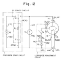
- the discharge start circuit as a third embodiment, as shown in Fig. 12, comprises a discharge start voltage source V T and an RC series circuit arranged in parallel.
- a first terminal V70 of the discharge start voltage source V T will be electrically connected to the second terminal RC40 of the RC series circuit through the trigger switch S T
- a second terminal V80 of the discharge start voltage source V T is electrically connected to the first and second cathode terminals 152 and 162.
- a first terminal RC30 of the RC series circuit is electrically connected to the first and second cathode terminals 152 and 162, and a second terminal RC40 will be electrically connected to one of the anode terminal 142 and the first terminal V70 of the discharge start voltage source V T through the trigger switch S T .
- the cathode heating voltage source V F supplies a predetermined voltage to the hot cathode for heating the hot cathode
- the discharge start voltage source V0 supplies a predetermined voltage between the anode and the hot cathode.
- the discharge start circuit supplies a predetermined voltage sufficient to generate discharge between the hot cathode and one of the focusing electrode and the anode, to one of the focusing electrode and the anode.
- the luminance adjustment circuit adjustments a potential of the focusing electrode by supplying a predetermined voltage so as to set the potential of the focusing electrode zero or negative.
- the focusing electrode is electrically insulated from the cathode slit electrode and the front electrode.
- the luminance adjustment circuit constituted by the luminance adjustment voltage source, the variable resistor, and the luminance adjustment switch, all of which are sequentially arranged in series, is arranged between the hot cathode and the focusing electrode.
- Fig. 1 is a perspective view showing a gas discharge tube according to the present invention.
- Fig. 2 is an exploded perspective view of a light-emitting portion of the gas discharge tube 20 in Fig. 1.
- Fig. 3 is a perspective view showing a discharge shielding member and an anode in the light-emitting portion in Fig. 2 before assembly.
- Fig. 4 is a perspective view showing a support member and the anode in the light-emitting portion in Fig. 2 before assembly.
- Fig. 5 is a plan view showing a positional relationship among the discharge shielding member, the anode, and the support member in the light-emitting portion in Fig. 2.
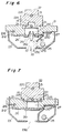
- Fig. 6 is a sectional view taken along a line A - A in Fig. 5.
- Fig. 7 is a sectional view taken along a line B - B in Fig. 5.
- Fig.8 is a sectional view for explaining a structure of the recessed portion of the discharge shielding member in Fig. 3.
- Fig. 9 is a circuit diagram showing a lighting device for the gas discharge tube in Fig.1, as a first embodiment of the present invention.
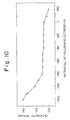
- Fig. 10 is a graph showing a relationship between the potential of a focusing electrode of the gas discharge tube in Fig. 1 and an optical output.
- Fig. 11 is a circuit diagram showing the lighting device for the gas discharge tube in Fig. 1, as a second embodiment of the present invention.
- Fig. 12 is a circuit diagram showing the lighting device for the gas discharge tube in Fig. 1, as a third embodiment of the invention.
- gas discharge tube of this embodiment is a side-on type deuterium discharge tube which extracts light (U.V) from the side portion of the tube.
- a light-emitting section 20 is accommodated in a glass envelope 11 while being supported by lead pins 13 to 16.
- Deuterium gas in the glass envelope 11 is sealed at about several Torr.
- the envelop 11 with its head portion sealed has a cylindrical shape, and the bottom portion of the envelope 11 is hermetically sealed by a glass stem 12.
- the envelop 11 is formed of ultraviolet light transmitting glass or quartz glass having a high permeability to ultraviolet light.
- the four lead pins 13 to 16 which are in parallel aligned in line extend through the glass stem 12 from the bottom portion of the light-emitting section 20, and are covered by insulating members 130, 140, 150, and 160, respectively. Terminals 131, 141, 151, and 161 will be connected to terminals 132, 142, 152, and 162 of an external power supply.
- the light-emitting section 20 has a shielding box structure in which a ceramic support member 22 and a metal front electrode 23 are bonded each other while a ceramic discharge shielding member (spacer) 21 is sandwiched therebetween.
- the anode plate 24 is sandwiched by the discharge shielding member 21 and the support member 22, and is accommodated in a space defined by these members 21 and 22.
- the embodiments of this invention relate to for example U.S.Patent Application No. 08/305,972, Japanese Patent Laid-Open No. 4-255662, and the like. Particularly, a basic structure of the gas discharge tube and materials of members such as anode, etc. are described in these references.
- the discharge shielding member 21 and the support member 22 are made of ceramic as insulator, and the anode plate 24 is made of molybdenum as high melting point metal.
- the high melting metal means material group having a higher melting point than sillicon (1414°C).
- the flat plate-like discharge shielding member 21 has a swell section thinner and wider than the support member 22.
- the discharge shielding member 21 has a through hole 210, a recessed portion 211, a vertical through hole 212, four horizontal through holes 213, two horizontal through holes 214 and four horizontal through holes 215.
- the through hole 210 extends through the discharge shielding member 21 almost at its central portion to oppose the anode 24.
- the recessed portion 211 is recessed from the rear surface 21B of the discharge shielding member 21.
- the recessed portion 211 also includes an opening edge portion located on the rear surface side of the through hole 210.
- the vertical through hole 212 extends in the vertical direction with respect to the bottom surface 11A of the envelope 11, and passes through the discharge shielding member 21.
- the four horizontal through holes 213 respectively extend in the horizontal direction with respect to the bottom surface 11A of the envelope 11.
- the two horizontal through holes 214 of the discharge shielding member 21 are formed at positions to insert lock pawls 271 of a cathode slit electrode 27 (to be described later).
- the four horizontal through holes 215 are formed at positions to insert lock pawls 231 of the front electrode 23 (to be described later).
- Electrode rods 250 and 251 are welded to the two ends of a hot cathode (filament) 25.
- the electrode rod 250 is welded to the distal end of the electrode rod 216, and the electrode rod 251 is welded to the distal end of the lead pin 16. With this structure, the hot cathode 25 will be held by the stem 12.
- the support member 22 is a prism having a swell section 22A.
- a vertical through hole 220, concave grooves 221 to 223, a depression 224, four protrusions portions (projections 225), and four horizontal through holes 226 are formed in the support member 22.
- the vertical through hole 220 vertically extends in the vertical direction with respect to the bottom surface 11A of the envelope 11, and passes through the section 22A of the support member 22.
- the concave grooves 221 to 223 and the depression 224 are recessed on the front surface 22B of the support member 22 and sequentially extend toward the bottom surface 11A of the envelop 11, thereby appropriately accommodating the lead pin 14 and an insulating member 141.
- the four projections 225 are formed close to the opening edge portions of the concave grooves 221 and 222 and project from the front surface 22B of the support member 22 so as to oppose the corners of an anode plate 24.
- the four horizontal through holes 226 extend in the horizontal direction to oppose four the horizontal through holes 213 of the discharge shielding 21.
- the support member 22 is held by the glass stem 12 through the lead pin 13 inserted in the vertical through hole 220 and the lead pin 14 accommodated in the concave grooves 221 to 223.
- the rectangular flat plate-like anode 24 is welded and fixed to the distal end of the lead pin 14 and pushed onto the rear surface side of the discharge shielding member 21 by the four projections 225 of the support member 22.
- a heat dissipation space is ensured at the back of the anode 24 by providing the depression 224 having an opening substantially matching the surface area of the anode 24.
- the rectangular anode 24 indicated by a broken line is accommodated in the recessed portion 211 of the discharge shielding member 21.
- the corner portions of the anode 24 are sandwiched by cooperation of the bottom surface 11A of the step portion 211 of the discharge shielding member 21 and the four projections 225 of the support member 22.
- the four sides of the anode 24 almost match the slightly round through hole 210 having a substantially rectangular shape.
- the remaining portion of the opening edge portion of the through hole 210 is joined to the four corner portions of the anode 24.
- the four projections 225 each having a circular surface are joined to the four corner portions of the anode 24, thereby pressing the anode 24.
- the rectangular recessed portion 211 has a depth W21 matching the sum of the height W225 of the four projection 225 and the thickness W24 of the anode 24.
- each projection 225 is gripped by the projections 225 and the rear surface 21B of the discharge shielding member 21.
- the top surface of each projection 225 is defined by the part C3 contacting the associated part C4 of the anode plate 24 and other part facing the rear surface 21B of the discharge shielding member 21 without through the anode plate 24.
- this structure increase the heat racdiatio efficiency of the anode plate 24 because a specific area of the anode plate 24 decreases, the area being directly contact with insulator (the discharge shielding member 21, the support member 22, etc.) having a lower heat conductivity decreases.
- a focusing electrode 26 constituted by bending a metal plate into a substantially L-shape and an opening limit plate 261, and has an opening 260 and four horizontal through holes 263.
- the focusing opening 260 is arranged coaxial with the through hole 210 of the discharge shielding plate 21.
- An opening limit plate 261 for limiting the diameter of the opening is welded to the peripheral region of the opening 260.
- the opening limit plate 261 has a focusing opening 262 bent toward the anode 24 to pass through the opening 260.
- the four horizontal through holes 263 extend in the direction of thickness of the focusing electrode 26 and oppose the four horizontal through holes of the discharge shielding member 21.
- the focusing electrode 26 is arranged so as to be in contact with the front surface 21A of the discharge shielding member 21. Since a distal end portion 26A bent backward is welded to the distal end of the lead pin 13 projecting from the support member 22, the focusing electrode 26 is fixed to the discharge shielding member 21 and the support member 22. Note that the distance between the opening limit plate 261 and the anode 24 is smaller than the thickness of the discharge shielding member 21.
- the horizontal through holes 226 of the support member 22, the horizontal through holes 213 of the discharge shielding member 21, and the horizontal through holes 263 of the focusing electrode 26 are aligned in line. Therefore, when the discharge shielding member 21, the support member 22, and the focusing electrode 26 are bonded each other, and four metal rivets 28 are inserted into the through holes, all these components will be integrally fixed to the stem 12.
- the cathode slit electrode 27 is bent at three portions in correspondence with the shape of the stepped portion 217 of the discharge shielding member 21 and has an opening (slit 270) and two lock pawls 271.
- the opening 270 having a vertically elongated rectangular shape extends through the cathode slit electrode 27.
- the two lock pawls 271 formed at the upper and lower ends of the cathode slit electrode 27 are bent backward.
- the cathode slit electrode 27 opposes the hot cathode 25 and is positioned in front surface side of the discharge shielding member 21 on its one side.
- the cathode slit electrode 27 is engaged with the discharge shielding member 21.
- the slit 270 is arranged between the hot cathode 25 and the opening limit plate 261.
- the metal front electrode 23 is bent at four portions to have a substantially U-shaped section and has an opening window 230 and four lock pawls 231.
- the rectangular opening window 230 is arranged coaxial with the focusing opening 262 of the focusing electrode 26.
- the four lock pawls 231 formed at the corners of the front electrode 23 project backward. Note that the opening window 230 is arranged at a position to project ultraviolet light from the space in front of or near the focusing opening 262.
- the front electrode 23 is arranged at the front surface 21A of the discharge shielding member 21 on its both sides.
- the front electrode 23 is engaging with the discharge shielding member 21.
- the front end of the cathode slit electrode 27 is brought into contact with the inner wall of the front electrode 23, thereby separating a space where the hot cathode 25 is arranged from a light-emitting space where arc discharge occurs.
- a predetermined rated voltage is applied to the hot cathode 25, and the hot cathode 25 is preheated.
- a DC open voltage of about 150 V is applied between the hot cathode 25 and the anode 24.
- thermoelectrons moving in a direction indicated by an arrow 30 is limited to only a discharge path 31 because of the convergent effect of the opening limit plate 261 of the focusing electrode 26 and the shielding effect of the cathode slit electrode 27 and the front electrode 23.
- thermoelectrons emitted from the hot cathode 25 pass through the focusing opening 262 of the opening limit plate 261 from the slit 270 of the cathode slit electrode 27 and through the through hole 210 of the discharge shielding member 21 and are received by the anode 24.
- An arc ball 32 as a high-density discharge area by arc discharge is generated in a space in front of or near the opening limit plate 261 on the opposite side to the anode 24 through the discharge shielding member 21.
- Ultraviolet light (U.V) extracted from the arc ball 32 as positive column light emission is emitted toward the front of the anode 24, i.e., in a direction indicated by an arrow 33 and is projected through the opening window 230 of the front electrode 23.
- the anode 24 and the focusing electrode 26 are arranged so as to be in contact with the two opening edge portions of the through hole 210 through the discharge shielding member 21. For this reason, the insulated state between the two electrodes 24 and 26 is maintained by the insulating properties of the material of the discharge shielding member 21. Upon occurrence of arc discharge, the anode 24 receives thermoelectrons to generate heat, and the focusing electrode 26 also generates heat upon bombardment of cations.
- the through hole 210 of the discharge shielding member 21 hardly covers the front surface 24A of the anode 24, and the front surface 24A of the anode 24 is exposed at maximum.
- the projections 225 of the support plate 22 are hardly in contact with the rear surface 24B of the anode 24, and the rear surface 24B of the anode 24 is exposed at maximum.
- the depression portion 224 of the support member 22 enlarges the back space of the anode 24. For this reason, heat dissipation from the anode 24 and the focusing electrode 26 is promoted.
- the material constituting the discharge shielding member 21 and the support member 22 and having electrical insulating properties generally has a low thermal conductivity, the temperature in the space near the anode 24 and the focusing electrode 26 can be maintained relatively low.
- the anode 24 and the focusing electrode 26 of the present invention deformation of the material due to a residual stress in a high temperature state, or a loss of the material due to an evaporation or sputtering phenomenon can be minimized. More specifically, a variation in distance between the two electrodes or energization hardly makes the arc discharge state unstable. Additionally, a loss of the material of the two electrodes hardly makes it difficult to generate arc discharge. Therefore, for long-time continuous light emission, the positions of the anode 24 and the focusing electrode 26 are precisely held, thereby realizing a continuously stable operation for a long time.
- the focusing electrode 26 is electrically insulated from the cathode slit electrode 27 and the front electrode 23 through the discharge shielding member 21.
- the cathode slit electrode 27 and the front electrode 23 are in contact with each other and set at the same potential, for example a zero potential.
- this lighting device is constituted as an auxiliary electrode system.
- the lighting device has an anode terminal 142 to be connected to the terminal 141 fixed at the distal end of lead pin 14, a focusing electrode terminal 132 to be connected to the terminal 131 fixed at the distal end of the lead pin 13, a first cathode terminal 152 to be connected to the terminal 151 fixed at the distal end of the lead pin 15, and a second cathode terminal 162 to be connected to the terminal 161 fixed at the distal end of the lead pin 16.
- a cathode heating voltage source (V F ) is disposed, and the first terminal V30 and the second terminal V40 of the cathode heating voltage source V F are respectively connected to the first and second cathode terminals 152 and 162.
- An electric field generating voltage source V0 is disposed between the hot cathode (E C ) 25 and the anode (E A ) 24, and the first terminal V10 and the second terminal V20 of the electric field generating voltage source V0 are respectively connected to the anode terminal 142 and the first and second cathode terminals 152 and 162.
- the cathode 25 is set at a voltage of about 2.5 V as a cathode filament rated value.
- the electric field generating voltage source V0 supplies a DC open voltage of about 150 V and a constant current of about 300 mA.
- an RC parallel circuit constituted by a capacitor C and a fixed resistor R C which are connected in parallel to each other and a trigger switch S T connected in series with the above circuit are disposed between the anode (E A ) 24 and the focusing electrode (E R ) 26.
- the first terminal RC10 of the RC parallel circuit will be connected to the focusing electrode terminal 132 through a luminance adjustment switch S A
- the second terminal RC20 of the RC parallel circuit will be connected to the anode terminal 142 through the trigger switch S T .
- the trigger switch S T functions to electrically connect the second terminal RC20 of the RC parallel circuit to the anode terminal 142
- the luminance adjustment switch S A functions to electrically connect the first terminal RC10 of the RC parallel circuit to the focusing electrode terminal 132 at a predetermined timing.
- a luminance adjustment voltage source V A and a variable resistor R V are disposed in series between the hot cathode (E C ) 25 and the focusing electrode (E R ) 26.
- the first terminal V50 of the luminance adjustment voltage source V A is connected to the first and second terminals 152 and 162, and the second terminal R20 of the variable resistor R V will be connected to the focusing electrode terminal 132 through the luminance adjustment switch S A . Therefore, the luminance adjustment switch S A also functions to connect the second terminal R20 of the variable resistor R V to the focusing electrode terminal 132 at a predetermined timing.
- the trigger switch S T is set in an OFF state, and the luminance adjustment switch S A is set in an ON state with respect to the discharge start circuit.
- a voltage of about 2.5 V is applied from the cathode heating voltage source V F to ends of the hot cathode (E C ) 25 for about 20 seconds before discharge, and the hot cathode (E C ) 25 is preheated.
- a voltage of about 150 V is applied between the hot cathode (E C ) 25 and the anode (E A ) 24 from the electric field generating voltage source V0, thereby generating an electric field from the anode (E A ) 24 to the hot cathode (E C ) 25.
- the trigger switch S T Upon completion of preparation of trigger discharge, the trigger switch S T is set in an ON state. With this operation, a potential of about 150 V is supplied from the electric field generating voltage source V0 to the focusing electrode (E R ) 26 through the capacitor C and the fixed resistor R C (RC parallel circuit), which are connected in parallel to each other, thereby generating trigger discharge between the hot cathode (E C ) 25 and the focusing electrode (E R ) 26.
- a positive potential higher than that of the cathode slit electrode 27 and the front electrode 23, both of which are set at about 0 V, can be supplied to the focusing electrode (E R ) 26.
- a trigger discharge area 30 extending from the hot cathode (E C ) 25 extends from a space surrounded by the front electrode 23 and the cathode slit electrode 27, i.e, a space in the cathode box to reach the focusing electrode (E R ) 26. Therefore, trigger discharge is generated between the hot cathode (E C ) 25 and the focusing electrode (E R ) 26, so that the gas discharge tube 10 is properly lighted.
- arc discharge is generated between the hot cathode (E C ) 25 and the anode (E A ) 24.
- the arc discharge stably continues on the basis of a current of about 300 mA, which is supplied between the hot cathode (E C ) 25 and the anode (E A ) 24 from the electric field generating voltage source V0.
- thermoelectrons is limited to only one discharge path because of the convergent effect of the opening limit plate 261 of the focusing electrode (E R ) 26 and the shielding effect of the cathode slit electrode 27 and the front window electrode 23. More specifically, the thermoelectrons emitted from the hot cathode (E C ) 25 pass through the focusing opening 262 of the opening limit plate 261 from the focusing opening 270 of the cathode slit electrode 27 and through the through hole 210 of the discharge shielding member 21 and are received by the anode (E A ) 24.
- An arc ball as a high-density discharge area by arc discharge is generated in a space in front of the opening limit plate 261 on the opposite side to the anode (E A ) 24.
- Ultraviolet light (U.V) extracted from the arc ball as positive column light emission is projected toward the front of the anode 24 through the opening window 230 of the front electrode 23.
- the luminance adjustment switch S A Upon occurrence of arc discharge, the luminance adjustment switch S A is set in an ON state with respect to the luminance adjustment circuit. With this operation, a potential of 0 V or a negative potential is supplied from the luminance adjustment voltage source V A to the focusing electrode (E R ) 26 through the variable resistor R V .
- the focusing electrode (E R ) 26 repels electrons and attracts cations.
- discharge start voltages For the gas discharge tube of this embodiment and a conventional gas discharge tube, trigger voltages required to be applied to the focusing electrodes for trigger discharge, i.e., discharge start voltages were measured.
- the discharge start voltage for the gas discharge tube of this embodiment was 90 to 100 V while that for the conventional gas discharge tube was 130 to 170 V.
- the discharge start voltage is included within a small variation range, and it is found that lighting is highly facilitated.
- the potential of the focusing electrode was changed on the basis of the resistance value of the variable resistor after lighting, and an optical output extracted from the positive column light emission was measured.
- a positive potential of about 34 V is supplied to the focusing electrode from the luminance adjustment circuit.
- an optical output value corresponding to the potential of about 34 V is defined as 100%, and an optical output value corresponding to each potential of the focusing electrode is normalized and plotted.
- the amount of an increase in optical output is almost 10% when the potential of the focusing electrode is 0 V.
- the amount of an increase in optical output reaches almost 40% when the potential of the focusing electrode is -120 V. Therefore, it is found that, in the gas discharge tube of this embodiment, the light emission intensity will be easily adjusted and increased.
- the arrangement and function of a second embodiment of the lighting device for the gas discharge tube according to the present invention will be described below with reference to Fig. 11.
- the lighting device of this embodiment is different from the above embodiment (Fig. 9) only in the discharge start circuit.
- this lighting device is constituted as an auxiliary electrode system.
- the discharge start circuit is also disposed between the anode (E A ) 24 and the hot cathode (E C ) 25, and constituted by the fixed resistor R C and the capacitor C.
- the first terminal R30 of the fixed resistor R C is connected to the anode terminal 142, the second terminal R40 will be connected to the capacitor C through the trigger switch S T .
- the first terminal C10 is connected to the first and second cathode terminals 152 and 162, and the second terminal C20 will be connected to one of the fixed resistor R C and the focusing electrode terminal 132 through the trigger switch S T and the luminance adjustment switch S A .
- the trigger switch S T functions to connect the capacitor C to one of the fixed resistor R C and the luminance adjustment switch S A
- the luminance adjustment switch S A functions to connect the focusing electrode terminal 132 to one of the trigger switch S T and the luminance adjustment circuit.
- the trigger switch S T and the luminance adjustment switch S A are set in an ON state with respect to the discharge start circuit, and thereafter, preparation for trigger discharge is made in the same manner as in the above embodiment.
- a voltage of about 150 V is applied from the electric field generating voltage source V0 to the capacitor C through the fixed resistor R C , and the capacitor C is sufficiently charged.
- the trigger switch S T is set in an ON state with respect to the focusing electrode (E R ) 26, thereby supplying a potential of about 150 V to the focusing electrode (E R ) 26 by a pulse voltage based on discharge of the capacitor C.
- trigger discharge occurs between the hot cathode (E C ) 25 and the focusing electrode (E R ) 26.
- the arrangement and function of the third embodiment of the lighting device for the gas discharge tube according to the present invention will be described below with reference to Fig. 12.
- the lighting device of this embodiment is different from the above embodiment (Fig. 9) only in the discharge start circuit.
- this lighting device is not constituted as a normal auxiliary electrode system.
- the discharge start circuit and the discharge start circuit is constituted by a discharge start voltage source V T and an RC series circuit.
- a first terminal V70 of the discharge start voltage source V T will be connected to the RC series circuit through the trigger switch S T
- a second terminal V80 is connected to the first and the second cathode terminals 152 and 162.
- a first terminal RC30 of the RC series circuit will be connected to one of the discharge start voltage source V T and the anode terminal 142 through the trigger switch S T .
- the trigger switch S T functions to connect the second terminal RC40 of the RC series circuit one of the first terminal V70 and the anode terminal 142 at a predetermined timing.
- the discharge start voltage source V T supplies a DC open voltage of about 500 to 650 V.
- the luminance adjustment switch S A functions to connect the second terminal R20 of the luminance adjustment circuit to the focusing electrode terminal 132 at a predetermined timing.
- the trigger switch S T is set in an ON state with respect to the discharge start circuit, and at the same time, the luminance adjustment switch S A is set in an OFF state. Thereafter, preparation for trigger discharge is made in the same manner as in the above embodiment. At this time, a voltage of 500 to 650 V is applied from the discharge start voltage source V T to the capacitor C through the fixed resistor R C , and the capacitor C is sufficiently charged.
- the trigger switch S T is set in an ON state with respect to the anode (E A ) 24, thereby supplying a potential of about 500 to 650 V to the anode (E A ) 24 by a high pulse voltage based on discharge of the capacitor C.
- trigger discharge occurs between the hot cathode (E C ) 25 and the anode (E A ) 24 on the basis of a reduced impedance.
- the trigger voltage to be applied between the anode (E A ) 24 and the hot cathode (E C ) 25 is set to about 500 to 650 V in consideration of the reliability.
- the light-emitting section is constituted as a side-on type which extracts light from the side portion of the tube.
- a head-on type light-emitting portion which extracts light from the head portion of the tube, the same effect as in the above embodiment can be obtained.
- a normal ceramic As the material of the discharge shielding member and the support member, a normal ceramic is used.
- a so-called conductive ceramic such as beryllium oxide or aluminum nitride having a high thermal conductivity is used as the material of the discharge shielding member and the support member, a sink tank for the anode which is heated to a high temperature due to self heat generation is formed. For this reason, dissipation of the heat accumulated in the light-emitting section is promoted, and the operation of the gas discharge tube can be stabilized.
- the focusing electrode is electrically insulated from the cathode slit electrode and the front electrode.
- the luminance adjustment circuit constituted by the luminance adjustment voltage source, the variable resistor, and the luminance adjustment switch, all of which are sequentially connected in series, is arranged between the hot cathode and the focusing electrode.
Landscapes
- Physics & Mathematics (AREA)
- Spectroscopy & Molecular Physics (AREA)
- General Physics & Mathematics (AREA)
- Vessels And Coating Films For Discharge Lamps (AREA)
- Discharge Lamp (AREA)
Abstract
Description
- The present invention relates to a gas discharge tube used as an ultraviolet light source for a spectrophotometer, liquid chromatography, or the like, a lighting device therefor, and a method of operating the lighting device.
- A gas discharge tube is a discharge light source using positive column light emission by arc discharge of a gas sealed in a tube. As a typical gas discharge tube, a deuterium discharge tube in which ultraviolet light is emitted by discharge of sealed deuterium is well known. This deuterium discharge tube is mainly used as an ultraviolet continuous spectrum source for a spectrophotometer or the like. Note that a deuterium discharge tube having a light-emitting portion is described in, e.g., Japanese Utility Model Laid-Open No. 60-29400.
- It is an object of the present invention to provide a gas discharge tube which is properly lighted to improve the reproducibility of a satisfactory light emission state. It is another object of the present invention to provide a method of operating a lighting device for a gas discharge tube and a lighting device for a gas discharge tube, which maintain stable discharge and increases a light emission intensity.
- In order to achieve the objects, as shown in Fig. 1, a
gas discharge tube 10 of the present invention comprises: an glass envelope 11 for sealing a gas therein;lead pins 13 to 16 introduced into an inner space of the envelope 11 from external of the envelope 11; and a light-emitting section 20 in the glass envelope 11, positioned at distal ends of thelead pins 13 to 16 and supported by these lead pins while spaced from an inner side wall of the glass envelope 11. Theanode 24 is a metal plate mounted on and supported by the distal end of thelead pin 14. - In particular, as shown in Figs.2, 6, and 7, the light-
emitting section 20 includes: adischarge shielding member 21 of an insulator, such as a ceramic, having afront surface 21A and arear surface 21B which is opposite to thefront surface 21A; ahot cathode 25 for emitting thermoelectrons, positioned at the front surface side of thedischarge shielding member 21; ananode 24 for receiving the thermoelectrons emitted from saidhot cathode 25, mounted on and supported by therear surface 21B of thedischarge shielding member 21; a focusingelectrode 26 having a focusing opening 262 for converging paths of the thermoelectrons and for passing through the thermoelectrons which is emitted from thehot cathode 25 and which is received by theanode 24; and a cathode box surrounding thehot cathode 25, for partially shielding discharge of thehot cathode 25. The cathode box is mounted on and supported by thefront surface 21A of thedischarge shielding member 21, and is electrically insulated from the focusingelectrode 26. The cathode box is constituted by: acathode slit electrode 27 located between thehot cathode 25 and the focusingelectrode 26, having aslit 270 for passing through the thermoelectrons emitted from thehot cathode 25, and afront electrode 23 facing to the focusingelectrode 26 so as to accommodate thehot cathode 25 and thecathode slit electrode 27 in a space defined by thefront electrode 23 and the focusingelectrode 26, thefront electrode 23 having anopening window 230 located at a position which faces to the focusing opening 262 of the focusingelectrode 26, for outputting ultraviolet light (U.V) caused by discharge. And, the cathode slitelectrode 27 and thefront electrode 23 of the cathode box are in directly contact with each other, thereby each electrode has a same potential. - Furthermore, as shown in Fig. 3, the
discharge shielding member 21 has arecessed portion 211 at therear surface 21B of thedischarge shielding member 21, for accommodating theanode plate 24. As shown in Fig. 8, therecessed portion 211 of thedischarge shielding member 21 has a depth W21 matching a sum of a height W225 of theprojections 225 of thesupport member 21 and a thickness W24 of theanode 24, thereby thefront surface 22B of thesupport member 22 is in partially contact with therear surface 21B of thedischarge shielding member 21. Thedischarge shielding member 21 is in contact with parts C2 (see Fig.4) of theanode plate 24 at parts C1 of therear surface 21B of saiddischarge shielding member 21. Therefore, theanode plate 24 covers an opening of the throughhole 210 at the rear surface side of thedischarge shielding member 21. The focusingelectrode 26 is also supported by thedischarge shielding member 21 and in contact with thefront surface 21A of thedischarge shielding member 21, thereby a distance between the focusingelectrode 26 and theanode plate 24 is kept at a constact distance. - The light-emitting section, as shown in Figs. 2 and 4, further comprises a
support member 22 of an insulator, such as a ceramic, being in the glass envelope 11 and located on an opposite side to thedischarge shielding member 21 through theanode plate 24, thesupport member 22 havingprojections 225 for pushing parts C4 of theanode plate 24 onto parts C1 of therear surface 21B of thedischarge shielding member 21. Therefore, the parts C1 of thedischarge shielding member 21 are brought into contact with the parts C2 of theanode plate 24, and the parts C3 of thesupport member 22 are brought into contact with the parts C4 of theanode plate 24. Particularly, a top surface of eachprojection 225 contains the part C3 contacting the associated part C4 of theanode plate 24, but other part of the top surface of eachprojection 225 faces therear surface 21B of thedischarge shielding member 21 without through theanode plate 24. As a result, theanode plate 24 is gripped at a plurality of parts thereof, and the present invention obtains a structure that is effective to increase the heat radiation efficiency of the anode plate. In other words, this structure decreases area contacting insulator having a lower heat conductivity. - The
support member 22 further has adepression 224 at afront surface 22B which faces to therear surface 24B of theanode 24, thereby thedepression 224 of thesupport member 22 provides heat dissipation space for theanode 24. - Next, as shown in Figs.9, 11, and 12, a lighting device for a gas discharge shielding of the present invention, for a gas discharge tube which has at least an anode, a focusing electrode, and a hot cathode, comprises: an anode terminal 142 adapted to be electrically connected to the anode of the gas discharge tube; a focusing electrode terminal 132 adapted to be electrically connected to the focusing electrode of the gas discharge tube; a first and second cathode terminals 152 and 162 adapted to be electrically connected to both ends of the hot cathode of the gas discharge tube; a cathode heating voltage source VF for heating the hot cathode, disposed between the first and second cathode terminals 152 and 162; an electric field generating voltage source V₀ for generating an electric field from the anode to the hot cathode of the gas discharge tube, disposed between the anode terminal 142 and the first and second cathode terminals 152 and 162; a discharge start circuit for supplying a trigger voltage to the focusing electrode in order to start discharge between the hot cathode and the focusing electrode; and a luminance adjustment circuit for adjusting a potential to be supplied to the focusing electrode of the gas discharge tube.
- A first terminal V10 of the electric field generating voltage source V₀ is electrically connected to the anode terminal 142, and a second terminal V20 of the electric field generating voltage source V₀ is electrically connected to the first and second cathode terminal 152 and 162. A first terminal V30 of the cathode heating voltage source VF is electrically connected to the first cathode terminal 152, and a second terminal V40 of the cathode heating voltage source VF is electrically connected to the second cathode terminal 162. Particularly, the luminance adjustment circuit is constituted by the luminance adjustment voltage source VA and the variable resistor RV arranged in series so that a second terminal V60 of the luminance adjustment voltage source VA and a first terminal R10 of the variable resistor RV are connected to each other. A first terminal V50 of the luminance adjustment voltage source VA is electrically connected to the first and second cathode terminal 152 and 162, and a second terminal R20 of the variable resistor RV will be electrically connected to the focusing electrode terminal 132 through a luminance adjustment switch SA.
- The discharge start circuit as a first embodiment, as shown in Fig. 9, comprises an RC parallel circuit disposed between the anode terminal 142 and the focusing electrode terminal 132. A first terminal RC10 of the RC parallel circuit will be electrically connected to the focusing electrode terminal 132 through the luminance adjustment switch SA, and a second
terminal RC 20 of the RC parallel circuit will be electrically connected to the anode terminal 142 through a trigger switch ST. - The discharge start circuit as a second embodiment, as shown in Fig.11, is constituted by a fixed resistor RC and a capacitor C. A first terminal R30 of the fixed resistor RC is electrically connected to the anode terminal 142, and a second terminal R40 of the fixed resistor RC will be connected to a second terminal C20 of the capacitor C. A first terminal C10 of the capacitor C is electrically connected to the first and second cathode terminals 152 and 162, and the second terminal C20 of the capacitor C will be electrically connected to one of the second terminal R40 of the fixed resistor RC and the focusing electrode terminal 132 through the trigger switch ST and the luminance adjustment switch SA.
- The discharge start circuit as a third embodiment, as shown in Fig. 12, comprises a discharge start voltage source VT and an RC series circuit arranged in parallel. A first terminal V70 of the discharge start voltage source VT will be electrically connected to the second terminal RC40 of the RC series circuit through the trigger switch ST, and a second terminal V80 of the discharge start voltage source VT is electrically connected to the first and second cathode terminals 152 and 162. A first terminal RC30 of the RC series circuit is electrically connected to the first and second cathode terminals 152 and 162, and a second terminal RC40 will be electrically connected to one of the anode terminal 142 and the first terminal V70 of the discharge start voltage source VT through the trigger switch ST.
- The operation for the above lighting device of the present invention is carried out tube as follows. First, the cathode heating voltage source VF supplies a predetermined voltage to the hot cathode for heating the hot cathode, sequentially (after the hot cathode has been heated) the discharge start voltage source V₀ supplies a predetermined voltage between the anode and the hot cathode. After an electric field is generated from the anode to the hot cathode, the discharge start circuit supplies a predetermined voltage sufficient to generate discharge between the hot cathode and one of the focusing electrode and the anode, to one of the focusing electrode and the anode. From now on, the luminance adjustment circuit adjustments a potential of the focusing electrode by supplying a predetermined voltage so as to set the potential of the focusing electrode zero or negative.
- In the gas discharge tube of the present invention, the focusing electrode is electrically insulated from the cathode slit electrode and the front electrode. With this structure, after the hot cathode is sufficiently heated, and a predetermined electric field is supplied to a space between the hot cathode and the anode, a positive potential higher than that of the front electrode and the cathode slit electrode will be supplied to the focusing electrode in generation of trigger discharge between the hot cathode and the focusing electrode. For this reason, the trigger discharge area extending from the cathode extends from a space surrounded by the front electrode and the cathode slit electrode, i.e., a space in the cathode box to reach the focusing electrode. Therefore, arc discharge will be easily generated between the hot cathode and the anode.
- In addition, in the lighting device for the gas discharge tube of the present invention, the luminance adjustment circuit constituted by the luminance adjustment voltage source, the variable resistor, and the luminance adjustment switch, all of which are sequentially arranged in series, is arranged between the hot cathode and the focusing electrode. With this arrangement, when the luminance adjustment switch is set in an ON state with respect to the luminance adjustment circuit upon occurrence of arc discharge, a zero potential or a negative potential will be supplied from the luminance adjustment voltage source to the focusing electrode through the variable resistor. Since the focusing electrode repels electrons and attracts cations, an ion sheath is generated in a space in front of or near the focusing electrode. Therefore, the arc ball can be compressed or focused by this ion sheath.
- The present invention will become more fully understood from the detailed description given hereinbelow and the accompanying drawings which are given by way of illustration only, and thus are not to be considered as limiting the present invention.
- Further scope of applicability of the present invention will become apparent from the detailed description given hereinafter. However, it should be understood that the detailed description and specific examples, while indicating preferred embodiments of the invention, are given by way of illustration only, since various changes and modifications within the spirit and scope of the invention will become apparent to those skilled in the art form this detailed description.
- Fig. 1 is a perspective view showing a gas discharge tube according to the present invention.
- Fig. 2 is an exploded perspective view of a light-emitting portion of the
gas discharge tube 20 in Fig. 1. - Fig. 3 is a perspective view showing a discharge shielding member and an anode in the light-emitting portion in Fig. 2 before assembly.
- Fig. 4 is a perspective view showing a support member and the anode in the light-emitting portion in Fig. 2 before assembly.
- Fig. 5 is a plan view showing a positional relationship among the discharge shielding member, the anode, and the support member in the light-emitting portion in Fig. 2.
- Fig. 6 is a sectional view taken along a line A - A in Fig. 5.
- Fig. 7 is a sectional view taken along a line B - B in Fig. 5.
- Fig.8 is a sectional view for explaining a structure of the recessed portion of the discharge shielding member in Fig. 3.
- Fig. 9 is a circuit diagram showing a lighting device for the gas discharge tube in Fig.1, as a first embodiment of the present invention.
- Fig. 10 is a graph showing a relationship between the potential of a focusing electrode of the gas discharge tube in Fig. 1 and an optical output.
- Fig. 11 is a circuit diagram showing the lighting device for the gas discharge tube in Fig. 1, as a second embodiment of the present invention.
- Fig. 12 is a circuit diagram showing the lighting device for the gas discharge tube in Fig. 1, as a third embodiment of the invention.
- The arrangement and function of a gas discharge tube according to the first embodiment of the present invention will be described below in detail with reference to Figs. 1 to 13. Note that the gas discharge tube of this embodiment is a side-on type deuterium discharge tube which extracts light (U.V) from the side portion of the tube.
- In a
gas discharge tube 10 shown in Fig. 1, a light-emittingsection 20 is accommodated in a glass envelope 11 while being supported bylead pins 13 to 16. Deuterium gas in the glass envelope 11 is sealed at about several Torr. The envelop 11 with its head portion sealed has a cylindrical shape, and the bottom portion of the envelope 11 is hermetically sealed by aglass stem 12. The envelop 11 is formed of ultraviolet light transmitting glass or quartz glass having a high permeability to ultraviolet light. - The four
lead pins 13 to 16 which are in parallel aligned in line extend through the glass stem 12 from the bottom portion of the light-emittingsection 20, and are covered by insulatingmembers Terminals section 20 has a shielding box structure in which aceramic support member 22 and ametal front electrode 23 are bonded each other while a ceramic discharge shielding member (spacer) 21 is sandwiched therebetween. Theanode plate 24 is sandwiched by thedischarge shielding member 21 and thesupport member 22, and is accommodated in a space defined by thesemembers - The embodiments of this invention relate to for example U.S.Patent Application No. 08/305,972, Japanese Patent Laid-Open No. 4-255662, and the like. Particularly, a basic structure of the gas discharge tube and materials of members such as anode, etc. are described in these references.
- For example, the
discharge shielding member 21 and thesupport member 22 are made of ceramic as insulator, and theanode plate 24 is made of molybdenum as high melting point metal. In this specification, the high melting metal means material group having a higher melting point than sillicon (1414°C). - The structure of the light-emitting
section 20 will be described below in detail with reference to Figs. 2 to 8. - As shown in Figs. 2 and 3, the flat plate-like
discharge shielding member 21 has a swell section thinner and wider than thesupport member 22. Thedischarge shielding member 21 has a throughhole 210, a recessedportion 211, a vertical throughhole 212, four horizontal throughholes 213, two horizontal throughholes 214 and four horizontal throughholes 215. The throughhole 210 extends through thedischarge shielding member 21 almost at its central portion to oppose theanode 24. The recessedportion 211 is recessed from therear surface 21B of thedischarge shielding member 21. The recessedportion 211 also includes an opening edge portion located on the rear surface side of the throughhole 210. The vertical throughhole 212 extends in the vertical direction with respect to the bottom surface 11A of the envelope 11, and passes through thedischarge shielding member 21. The four horizontal throughholes 213 respectively extend in the horizontal direction with respect to the bottom surface 11A of the envelope 11. The two horizontal throughholes 214 of thedischarge shielding member 21 are formed at positions to insertlock pawls 271 of a cathode slit electrode 27 (to be described later). The four horizontal throughholes 215 are formed at positions to insertlock pawls 231 of the front electrode 23 (to be described later). - One side of a substantially L-shaped
electrode rod 216 is inserted in the vertical throughhole 212, and the lower end of theelectrode rod 216 is exposed from thedischarge shielding member 21 so as to be welded to the distal end of thelead pin 15. Therefore, thedischarge shielding member 21 will be held by theglass stem 12 through theelectrode rod 216.Electrode rods electrode rod 250 is welded to the distal end of theelectrode rod 216, and theelectrode rod 251 is welded to the distal end of thelead pin 16. With this structure, thehot cathode 25 will be held by thestem 12. - As shown in Figs. 2 and 4, the
support member 22 is a prism having aswell section 22A. A vertical throughhole 220,concave grooves 221 to 223, adepression 224, four protrusions portions (projections 225), and four horizontal throughholes 226 are formed in thesupport member 22. The vertical throughhole 220 vertically extends in the vertical direction with respect to the bottom surface 11A of the envelope 11, and passes through thesection 22A of thesupport member 22. Theconcave grooves 221 to 223 and thedepression 224 are recessed on thefront surface 22B of thesupport member 22 and sequentially extend toward the bottom surface 11A of the envelop 11, thereby appropriately accommodating thelead pin 14 and an insulatingmember 141. The fourprojections 225 are formed close to the opening edge portions of theconcave grooves front surface 22B of thesupport member 22 so as to oppose the corners of ananode plate 24. The four horizontal throughholes 226 extend in the horizontal direction to oppose four the horizontal throughholes 213 of the discharge shielding 21. - The
support member 22 is held by theglass stem 12 through thelead pin 13 inserted in the vertical throughhole 220 and thelead pin 14 accommodated in theconcave grooves 221 to 223. The rectangular flat plate-like anode 24 is welded and fixed to the distal end of thelead pin 14 and pushed onto the rear surface side of thedischarge shielding member 21 by the fourprojections 225 of thesupport member 22. A heat dissipation space is ensured at the back of theanode 24 by providing thedepression 224 having an opening substantially matching the surface area of theanode 24. - As shown in Figs. 5, 7, and 8, the
rectangular anode 24 indicated by a broken line is accommodated in the recessedportion 211 of thedischarge shielding member 21. The corner portions of theanode 24 are sandwiched by cooperation of the bottom surface 11A of thestep portion 211 of thedischarge shielding member 21 and the fourprojections 225 of thesupport member 22. The four sides of theanode 24 almost match the slightly round throughhole 210 having a substantially rectangular shape. The remaining portion of the opening edge portion of the throughhole 210 is joined to the four corner portions of theanode 24. The fourprojections 225 each having a circular surface are joined to the four corner portions of theanode 24, thereby pressing theanode 24. In particular, as shown in Fig. 8, the rectangular recessedportion 211 has a depth W21 matching the sum of the height W225 of the fourprojection 225 and the thickness W24 of theanode 24. As a result, the peripheral portion formed on thefront surface 22B of thesupport member 22 will be brought into contact with therear surface 21B of thedischarge shielding member 21. - On the other hand, as shown in Figs. 3 and 4, the parts C1 of the
rear surface 21B of thedischarge shielding member 21 are brought into contact with the parts C2 of theanode plate 24, and the parts C3 of fthe top surface of eachprojection 225 are brought into contact with the parts C4 of theanode plate 24. Thereby, theanode plate 24 is gripped by theprojections 225 and therear surface 21B of thedischarge shielding member 21. The top surface of eachprojection 225 is defined by the part C3 contacting the associated part C4 of theanode plate 24 and other part facing therear surface 21B of thedischarge shielding member 21 without through theanode plate 24. That is, this structure increase the heat racdiatio efficiency of theanode plate 24 because a specific area of theanode plate 24 decreases, the area being directly contact with insulator (thedischarge shielding member 21, thesupport member 22, etc.) having a lower heat conductivity decreases. - As shown in Figs. 2 and 6, a focusing
electrode 26 constituted by bending a metal plate into a substantially L-shape and anopening limit plate 261, and has anopening 260 and four horizontal throughholes 263. The focusingopening 260 is arranged coaxial with the throughhole 210 of thedischarge shielding plate 21. Anopening limit plate 261 for limiting the diameter of the opening is welded to the peripheral region of theopening 260. Theopening limit plate 261 has a focusingopening 262 bent toward theanode 24 to pass through theopening 260. The four horizontal throughholes 263 extend in the direction of thickness of the focusingelectrode 26 and oppose the four horizontal through holes of thedischarge shielding member 21. - The focusing
electrode 26 is arranged so as to be in contact with thefront surface 21A of thedischarge shielding member 21. Since adistal end portion 26A bent backward is welded to the distal end of thelead pin 13 projecting from thesupport member 22, the focusingelectrode 26 is fixed to thedischarge shielding member 21 and thesupport member 22. Note that the distance between theopening limit plate 261 and theanode 24 is smaller than the thickness of thedischarge shielding member 21. The horizontal throughholes 226 of thesupport member 22, the horizontal throughholes 213 of thedischarge shielding member 21, and the horizontal throughholes 263 of the focusingelectrode 26 are aligned in line. Therefore, when thedischarge shielding member 21, thesupport member 22, and the focusingelectrode 26 are bonded each other, and fourmetal rivets 28 are inserted into the through holes, all these components will be integrally fixed to thestem 12. - As shown in Figs. 2, 6, and 7, the
cathode slit electrode 27 is bent at three portions in correspondence with the shape of the steppedportion 217 of thedischarge shielding member 21 and has an opening (slit 270) and twolock pawls 271. With respect to the bottom surface 11A of the envelope 11, theopening 270 having a vertically elongated rectangular shape extends through thecathode slit electrode 27. The twolock pawls 271 formed at the upper and lower ends of thecathode slit electrode 27 are bent backward. - The
cathode slit electrode 27 opposes thehot cathode 25 and is positioned in front surface side of thedischarge shielding member 21 on its one side. When the twolock pawls 271 are inserted into the two horizontal throughholes 214 of thedischarge shielding member 21, thecathode slit electrode 27 is engaged with thedischarge shielding member 21. Note that theslit 270 is arranged between thehot cathode 25 and theopening limit plate 261. - The
metal front electrode 23 is bent at four portions to have a substantially U-shaped section and has anopening window 230 and fourlock pawls 231. Therectangular opening window 230 is arranged coaxial with the focusingopening 262 of the focusingelectrode 26. The fourlock pawls 231 formed at the corners of thefront electrode 23 project backward. Note that theopening window 230 is arranged at a position to project ultraviolet light from the space in front of or near the focusingopening 262. - The
front electrode 23 is arranged at thefront surface 21A of thedischarge shielding member 21 on its both sides. When the fourlock pawls 231 are inserted into the four horizontal throughholes 215 of thedischarge shielding member 21, thefront electrode 23 is engaging with thedischarge shielding member 21. The front end of thecathode slit electrode 27 is brought into contact with the inner wall of thefront electrode 23, thereby separating a space where thehot cathode 25 is arranged from a light-emitting space where arc discharge occurs. - The operation of this embodiment will be described below.
- When a power of about 10 W is supplied from the external power supply in 20 seconds before discharge, a predetermined rated voltage is applied to the
hot cathode 25, and thehot cathode 25 is preheated. After thehot cathode 25 is sufficiently heated, a DC open voltage of about 150 V is applied between thehot cathode 25 and theanode 24. - Upon completion of preparation for arc discharge, a trigger voltage of 350 to 500 V is applied between the
hot cathode 25 and theanode 24, thereby starting arc discharge among thehot cathode 25, the focusingelectrode 26, and theanode 24. At this time, the path of thermoelectrons moving in a direction indicated by an arrow 30 is limited to only adischarge path 31 because of the convergent effect of theopening limit plate 261 of the focusingelectrode 26 and the shielding effect of thecathode slit electrode 27 and thefront electrode 23. More specifically, the thermoelectrons emitted from thehot cathode 25 pass through the focusingopening 262 of theopening limit plate 261 from theslit 270 of thecathode slit electrode 27 and through the throughhole 210 of thedischarge shielding member 21 and are received by theanode 24. - An
arc ball 32 as a high-density discharge area by arc discharge is generated in a space in front of or near theopening limit plate 261 on the opposite side to theanode 24 through thedischarge shielding member 21. Ultraviolet light (U.V) extracted from thearc ball 32 as positive column light emission is emitted toward the front of theanode 24, i.e., in a direction indicated by anarrow 33 and is projected through theopening window 230 of thefront electrode 23. - The
anode 24 and the focusingelectrode 26 are arranged so as to be in contact with the two opening edge portions of the throughhole 210 through thedischarge shielding member 21. For this reason, the insulated state between the twoelectrodes discharge shielding member 21. Upon occurrence of arc discharge, theanode 24 receives thermoelectrons to generate heat, and the focusingelectrode 26 also generates heat upon bombardment of cations. - However, the through
hole 210 of thedischarge shielding member 21 hardly covers thefront surface 24A of theanode 24, and thefront surface 24A of theanode 24 is exposed at maximum. Theprojections 225 of thesupport plate 22 are hardly in contact with therear surface 24B of theanode 24, and therear surface 24B of theanode 24 is exposed at maximum. Thedepression portion 224 of thesupport member 22 enlarges the back space of theanode 24. For this reason, heat dissipation from theanode 24 and the focusingelectrode 26 is promoted. Although the material constituting thedischarge shielding member 21 and thesupport member 22 and having electrical insulating properties generally has a low thermal conductivity, the temperature in the space near theanode 24 and the focusingelectrode 26 can be maintained relatively low. - As a result, for the
anode 24 and the focusingelectrode 26 of the present invention, deformation of the material due to a residual stress in a high temperature state, or a loss of the material due to an evaporation or sputtering phenomenon can be minimized. More specifically, a variation in distance between the two electrodes or energization hardly makes the arc discharge state unstable. Additionally, a loss of the material of the two electrodes hardly makes it difficult to generate arc discharge. Therefore, for long-time continuous light emission, the positions of theanode 24 and the focusingelectrode 26 are precisely held, thereby realizing a continuously stable operation for a long time. - In particular, in the focusing
electrode 26, thecathode slit electrode 27, and thefront electrode 23 having the above arrangement, the focusingelectrode 26 is electrically insulated from thecathode slit electrode 27 and thefront electrode 23 through thedischarge shielding member 21. On the other hand, thecathode slit electrode 27 and thefront electrode 23 are in contact with each other and set at the same potential, for example a zero potential. - The arrangement of a first embodiment of the lighting circuit connected to the gas discharge tube according to the present invention, will be described below with reference to Fig. 9.
- As shown in Fig. 9, this lighting device is constituted as an auxiliary electrode system. The lighting device has an anode terminal 142 to be connected to the terminal 141 fixed at the distal end of
lead pin 14, a focusing electrode terminal 132 to be connected to the terminal 131 fixed at the distal end of thelead pin 13, a first cathode terminal 152 to be connected to the terminal 151 fixed at the distal end of thelead pin 15, and a second cathode terminal 162 to be connected to the terminal 161 fixed at the distal end of thelead pin 16. Between ends of the hot cathode (EC), a cathode heating voltage source (VF) is disposed, and the first terminal V30 and the second terminal V40 of the cathode heating voltage source VF are respectively connected to the first and second cathode terminals 152 and 162. An electric field generating voltage source V₀ is disposed between the hot cathode (EC) 25 and the anode (EA) 24, and the first terminal V10 and the second terminal V20 of the electric field generating voltage source V₀ are respectively connected to the anode terminal 142 and the first and second cathode terminals 152 and 162. Note that thecathode 25 is set at a voltage of about 2.5 V as a cathode filament rated value. The electric field generating voltage source V₀ supplies a DC open voltage of about 150 V and a constant current of about 300 mA. - As a discharge start circuit, an RC parallel circuit constituted by a capacitor C and a fixed resistor RC which are connected in parallel to each other and a trigger switch ST connected in series with the above circuit are disposed between the anode (EA) 24 and the focusing electrode (ER) 26. The first terminal RC10 of the RC parallel circuit will be connected to the focusing electrode terminal 132 through a luminance adjustment switch SA, and the second terminal RC20 of the RC parallel circuit will be connected to the anode terminal 142 through the trigger switch ST. Therefore, the trigger switch ST functions to electrically connect the second terminal RC20 of the RC parallel circuit to the anode terminal 142, and the luminance adjustment switch SA functions to electrically connect the first terminal RC10 of the RC parallel circuit to the focusing electrode terminal 132 at a predetermined timing.
- As a luminance adjustment circuit, a luminance adjustment voltage source VA and a variable resistor RV are disposed in series between the hot cathode (EC) 25 and the focusing electrode (ER) 26. The first terminal V50 of the luminance adjustment voltage source VA is connected to the first and second terminals 152 and 162, and the second terminal R20 of the variable resistor RV will be connected to the focusing electrode terminal 132 through the luminance adjustment switch SA. Therefore, the luminance adjustment switch SA also functions to connect the second terminal R20 of the variable resistor RV to the focusing electrode terminal 132 at a predetermined timing.
- The operation of this embodiment will be described below.
- First of all, the trigger switch ST is set in an OFF state, and the luminance adjustment switch SA is set in an ON state with respect to the discharge start circuit. With this operation, a voltage of about 2.5 V is applied from the cathode heating voltage source VF to ends of the hot cathode (EC) 25 for about 20 seconds before discharge, and the hot cathode (EC) 25 is preheated. After the hot cathode (EC) 25 is sufficiently heated to a temperature of about 1,100°C, a voltage of about 150 V is applied between the hot cathode (EC) 25 and the anode (EA) 24 from the electric field generating voltage source V₀, thereby generating an electric field from the anode (EA) 24 to the hot cathode (EC) 25.
- Upon completion of preparation of trigger discharge, the trigger switch ST is set in an ON state. With this operation, a potential of about 150 V is supplied from the electric field generating voltage source V₀ to the focusing electrode (ER) 26 through the capacitor C and the fixed resistor RC (RC parallel circuit), which are connected in parallel to each other, thereby generating trigger discharge between the hot cathode (EC) 25 and the focusing electrode (ER) 26.
- Since the focusing electrode (ER) 26 is electrically insulated from the
cathode slit electrode 27 and thefront electrode 23, a positive potential higher than that of thecathode slit electrode 27 and thefront electrode 23, both of which are set at about 0 V, can be supplied to the focusing electrode (ER) 26. For this reason, as shown in Fig. 6, a trigger discharge area 30 extending from the hot cathode (EC) 25 extends from a space surrounded by thefront electrode 23 and thecathode slit electrode 27, i.e, a space in the cathode box to reach the focusing electrode (ER) 26. Therefore, trigger discharge is generated between the hot cathode (EC) 25 and the focusing electrode (ER) 26, so that thegas discharge tube 10 is properly lighted. - By generating trigger discharge in this manner, arc discharge is generated between the hot cathode (EC) 25 and the anode (EA) 24. The arc discharge stably continues on the basis of a current of about 300 mA, which is supplied between the hot cathode (EC) 25 and the anode (EA) 24 from the electric field generating voltage source V₀.
- At this time, the paths of thermoelectrons is limited to only one discharge path because of the convergent effect of the
opening limit plate 261 of the focusing electrode (ER) 26 and the shielding effect of thecathode slit electrode 27 and thefront window electrode 23. More specifically, the thermoelectrons emitted from the hot cathode (EC) 25 pass through the focusingopening 262 of theopening limit plate 261 from the focusingopening 270 of thecathode slit electrode 27 and through the throughhole 210 of thedischarge shielding member 21 and are received by the anode (EA) 24. - An arc ball as a high-density discharge area by arc discharge is generated in a space in front of the
opening limit plate 261 on the opposite side to the anode (EA) 24. Ultraviolet light (U.V) extracted from the arc ball as positive column light emission is projected toward the front of theanode 24 through theopening window 230 of thefront electrode 23. - Upon occurrence of arc discharge, the luminance adjustment switch SA is set in an ON state with respect to the luminance adjustment circuit. With this operation, a potential of 0 V or a negative potential is supplied from the luminance adjustment voltage source VA to the focusing electrode (ER) 26 through the variable resistor RV. The focusing electrode (ER) 26 repels electrons and attracts cations.
- At this time, since an ion sheath is generated in a space in front of the focusing electrode (ER) 26. the arc ball can be compressed or focused by this ion sheath. Therefore, when the resistance value of the variable resistor RV is appropriately set, the luminance of the
gas discharge tube 10 can be highly increased. - Experiments for this embodiment will be described below.
- For the gas discharge tube of this embodiment and a conventional gas discharge tube, trigger voltages required to be applied to the focusing electrodes for trigger discharge, i.e., discharge start voltages were measured. As a result, the discharge start voltage for the gas discharge tube of this embodiment was 90 to 100 V while that for the conventional gas discharge tube was 130 to 170 V. In the gas discharge tube of this embodiment, the discharge start voltage is included within a small variation range, and it is found that lighting is highly facilitated.
- In addition, for the gas discharge tube of this embodiment, pulse lighting was repeatedly performed. As a result, no lighting failure was observed. Therefore, it is found that the reliability of lighting of the gas discharge tube of this embodiment is highly improved.
- Furthermore, for the gas discharge tube of this embodiment, the potential of the focusing electrode was changed on the basis of the resistance value of the variable resistor after lighting, and an optical output extracted from the positive column light emission was measured. As a result, as shown in Fig. 10, when the potential of the focusing electrode increased in the negative direction, the optical output increased. In this case, however, a positive potential of about 34 V is supplied to the focusing electrode from the luminance adjustment circuit. In Fig. 10, an optical output value corresponding to the potential of about 34 V is defined as 100%, and an optical output value corresponding to each potential of the focusing electrode is normalized and plotted.
- As shown in Fig. 10, the amount of an increase in optical output is almost 10% when the potential of the focusing electrode is 0 V. The amount of an increase in optical output reaches almost 40% when the potential of the focusing electrode is -120 V. Therefore, it is found that, in the gas discharge tube of this embodiment, the light emission intensity will be easily adjusted and increased.
- The arrangement and function of a second embodiment of the lighting device for the gas discharge tube according to the present invention, will be described below with reference to Fig. 11. The lighting device of this embodiment is different from the above embodiment (Fig. 9) only in the discharge start circuit.
- As shown in Fig. 11, this lighting device is constituted as an auxiliary electrode system. The discharge start circuit is also disposed between the anode (EA) 24 and the hot cathode (EC) 25, and constituted by the fixed resistor RC and the capacitor C. The first terminal R30 of the fixed resistor RC is connected to the anode terminal 142, the second terminal R40 will be connected to the capacitor C through the trigger switch ST. The first terminal C10 is connected to the first and second cathode terminals 152 and 162, and the second terminal C20 will be connected to one of the fixed resistor RC and the focusing electrode terminal 132 through the trigger switch ST and the luminance adjustment switch SA. Therefore, the trigger switch ST functions to connect the capacitor C to one of the fixed resistor RC and the luminance adjustment switch SA, and the luminance adjustment switch SA functions to connect the focusing electrode terminal 132 to one of the trigger switch ST and the luminance adjustment circuit.
- According to this arrangement, first of all, the trigger switch ST and the luminance adjustment switch SA are set in an ON state with respect to the discharge start circuit, and thereafter, preparation for trigger discharge is made in the same manner as in the above embodiment. At this time, a voltage of about 150 V is applied from the electric field generating voltage source V₀ to the capacitor C through the fixed resistor RC, and the capacitor C is sufficiently charged.
- Subsequently, the trigger switch ST is set in an ON state with respect to the focusing electrode (ER) 26, thereby supplying a potential of about 150 V to the focusing electrode (ER) 26 by a pulse voltage based on discharge of the capacitor C. With this operation, trigger discharge occurs between the hot cathode (EC) 25 and the focusing electrode (ER) 26.
- After the trigger switch ST is set in an OFF state, generation of arc discharge and adjustment of the luminance are performed in the same manner as in the above embodiment.
- The arrangement and function of the third embodiment of the lighting device for the gas discharge tube according to the present invention, will be described below with reference to Fig. 12. The lighting device of this embodiment is different from the above embodiment (Fig. 9) only in the discharge start circuit.
- As shown in Fig. 12, this lighting device is not constituted as a normal auxiliary electrode system. Between the anode (EA) 24 and the hot cathode (EC) 25, the discharge start circuit, and the discharge start circuit is constituted by a discharge start voltage source VT and an RC series circuit. A first terminal V70 of the discharge start voltage source VT will be connected to the RC series circuit through the trigger switch ST, and a second terminal V80 is connected to the first and the second cathode terminals 152 and 162. A first terminal RC30 of the RC series circuit will be connected to one of the discharge start voltage source VT and the anode terminal 142 through the trigger switch ST. Therefore, the trigger switch ST functions to connect the second terminal RC40 of the RC series circuit one of the first terminal V70 and the anode terminal 142 at a predetermined timing. The discharge start voltage source VT supplies a DC open voltage of about 500 to 650 V. The luminance adjustment switch SA functions to connect the second terminal R20 of the luminance adjustment circuit to the focusing electrode terminal 132 at a predetermined timing.
- According to this arrangement, first of all, the trigger switch ST is set in an ON state with respect to the discharge start circuit, and at the same time, the luminance adjustment switch SA is set in an OFF state. Thereafter, preparation for trigger discharge is made in the same manner as in the above embodiment. At this time, a voltage of 500 to 650 V is applied from the discharge start voltage source VT to the capacitor C through the fixed resistor RC, and the capacitor C is sufficiently charged.
- Subsequently, the trigger switch ST is set in an ON state with respect to the anode (EA) 24, thereby supplying a potential of about 500 to 650 V to the anode (EA) 24 by a high pulse voltage based on discharge of the capacitor C. With this operation, trigger discharge occurs between the hot cathode (EC) 25 and the anode (EA) 24 on the basis of a reduced impedance.
- Although the discharge start voltage is about 350 at the start of lighting, the discharge start voltage increases according to continuation of lighting in some cases. For this reason, the trigger voltage to be applied between the anode (EA) 24 and the hot cathode (EC) 25 is set to about 500 to 650 V in consideration of the reliability.
- After the trigger switch ST is set in an OFF state, generation of arc discharge and adjustment of the luminance are performed in the same manner as in the above embodiment.
- Note that the present invention is not limited to the above embodiments, and various changes and modifications can also be made.
- In the above embodiment as to the gas discharge tube, the light-emitting section is constituted as a side-on type which extracts light from the side portion of the tube. However, with a head-on type light-emitting portion which extracts light from the head portion of the tube, the same effect as in the above embodiment can be obtained.
- In the above embodiment, as the material of the discharge shielding member and the support member, a normal ceramic is used. On the other hand, when a so-called conductive ceramic such as beryllium oxide or aluminum nitride having a high thermal conductivity is used as the material of the discharge shielding member and the support member, a sink tank for the anode which is heated to a high temperature due to self heat generation is formed. For this reason, dissipation of the heat accumulated in the light-emitting section is promoted, and the operation of the gas discharge tube can be stabilized.
- As has been described above in detail, in the gas discharge tube of the present invention, the focusing electrode is electrically insulated from the cathode slit electrode and the front electrode. With this structure, after the hot cathode is sufficiently heated, and a predetermined electric field is supplied to a space between the hot cathode and the anode, a positive potential higher than that of the front electrode and the cathode slit electrode will be supplied to the focusing electrode in generation of trigger discharge between the hot cathode and the focusing electrode. For this reason, the trigger discharge area extending from the cathode extends from a space surrounded by the front electrode and the cathode slit electrode, i.e., a space in the cathode box to reach the focusing electrode. Therefore, arc discharge will be easily generated between the hot cathode and the anode. Since this gas discharge tube will be certainly turned on, a gas discharge tube which improves the reproducibility of a satisfactory light emission state will be provided.
- In addition, in the lighting device for the gas discharge tube of the present invention, the luminance adjustment circuit constituted by the luminance adjustment voltage source, the variable resistor, and the luminance adjustment switch, all of which are sequentially connected in series, is arranged between the hot cathode and the focusing electrode. With this arrangement, when the luminance adjustment switch is set in an ON state with respect to the luminance adjustment circuit upon occurrence of arc discharge, a zero potential or a negative potential will be supplied from the luminance adjustment voltage source to the focusing electrode through the variable resistor. Since the focusing electrode repels electrons and attracts cations, an ion sheath is generated in a space in front of the focusing electrode. Therefore, the arc ball can be compressed or focused by this ion sheath. When the resistance value of the variable resistor is appropriately set, the luminance of the gas discharge tube will be increased. Therefore, a lighting device for a gas discharge tube, which highly increases the light emission intensity while maintaining stable discharge, will be provided.
- From the invention thus described, it will be obvious that the invention nay be varied in many ways. Such variations are not to be regarded as a departure from the spirit and scope of the invention, and all such modifications as would be obvious to one skilled in the art are intended to be included within the scope of the following claims. The basic Japanese Application No. 6-207714 (207714/1994) filed on August 31, 1994 is hereby incorporated by reference.
Claims (20)
- A gas discharge tube comprising:
an envelope for sealing a gas therein;
lead pins introduced into an inner space of said envelope from external of said envelope; and
a light-emitting section in said envelope, positioned at distal ends of said lead pins and supported by said lead pins while spaced from an inner side wall of said envelope, said light-emitting section including:
a hot cathode for emitting thermoelectrons;
an anode for receiving the thermoelectrons emitted from said hot cathode;
a focusing electrode having a focusing opening for converging paths of the thermoelectrons and for passing through the thermoelectrons which is emitted from said hot cathode and which is received by said anode; and
a cathode box surrounding said hot cathode, for partially shielding discharge of said hot cathode, said cathode box having
a cathode slit electrode located between said hot cathode and said focusing electrode, said cathode slit electrode having a slit for passing through the thermoelectrons emitted from said hot cathode, and
a front electrode facing to said focusing electrode so as to accommodate said hot cathode and said cathode slit electrode in a space defined by said front electrode and said focusing electrode, said front electrode having a window located at a position which faces to the focusing opening of said focusing electrode, for outputting light caused by discharge, wherein said cathode slit electrode and said front electrode are insulated from said focusing electrode. - A gas discharge tube according to claim 1, wherein said light-emitting section further comprises a discharge shielding member of an insulator positioned between said focusing electrode and said anode, and having a front surface and a rear surface which is opposite to the front surface, wherein
said focusing electrode is mounted on and supported by the front surface of said discharge shielding member, and wherein
said cathode slit electrode and said front electrode of said cathode box are respectively mounted on and supported by the front surface of said discharge shielding member while spaced from said focusing electrode. - A gas discharge tube according to claim 2, wherein said cathode slit electrode and said front electrode of said cathode box are in directly contact with each other so as to have a same potential.
- A gas discharge tube according to claim 1, wherein said light-emitting section further comprises a discharge shielding member of an insulator positioned between said focusing electrode and said anode, and having a front surface and a rear surface which is opposite to the front surface, wherein
said focusing electrode is mounted on and in contact with the front surface of said discharge shielding member, and
said anode is mounted on and in contact with the rear surface of said discharge shielding member. - A gas discharge tube according to claim 4, wherein said light-emitting section further comprises a support member of an insulator being in said envelope and located on an opposite side to said discharge shielding member through said anode, said support member having a projection for pushing said anode onto the rear surface of said discharge shielding member.
- A gas discharge tube according to claim 5, wherein said support member further has a depression at a surface which faces to said anode, for providing a heat dissipation space for said anode.
- A gas discharge tube according to claim 5, wherein said discharge shielding member and said support member are formed of a ceramic.
- A gas discharge tube according to claim 4, wherein said discharge shielding member has a recessed portion at the rear surface of said discharge shielding member, for accommodating said anode.
- A gas discharge tube according to claim 4, wherein said discharge shielding member is disposed in the inner space of said envelope while being supported by lead pins penetrating said envelope.
- A gas discharge tube according to claim 9, wherein said discharge shielding member is spaced from an inner side wall of said envelope through a space containing the gas.
- A gas discharge tube according to claim 9, wherein the recessed portion of said discharge shielding member has a depth matching a sum of a height of said projection of said support member and a thickness of said anode, whereby
a front surface of said support member is in partially contact with the rear surface of said discharge shielding member. - A gas discharge tube according to claim 1, wherein said anode is a metal plate mounted on and supported by a distal end of a lead pin penetrating said envelope.
- A lighting device for a gas discharge tube having at least a hot cathode for emitting thermoelectrons, an anode for receiving the thermoelectrons, and a focusing electrode for converging paths of the thermoelectrons, said lighting device comprising:
an anode terminal adapted to be electrically connected to the anode of the gas discharge tube;
a focusing electrode terminal adapted to be electrically connected to the focusing electrode of the gas discharge tube;
a first and a second cathode terminals adapted to be electrically connected to both ends of the hot cathode of the gas discharge tube;
an electric field generating voltage source for generating an electric field from the anode to the hot cathode of the gas discharge tube, disposed between said anode terminal and said first and second cathode terminals, having a first terminal being connected to said anode terminal and a second terminal being connected to said first and second cathode terminals; and
a luminance adjustment circuit for adjusting a potential to be supplied to the focusing electrode of the gas discharge tube, disposed between said focusing electrode terminal and said first and second cathode terminals, said luminance including:
a luminance adjustment voltage source having a first terminal being connected said first and second cathode terminals and a second terminal;
a variable resistor having a first terminal being connected to said second terminal of said luminance adjustment voltage source and a second terminal to be connected to said focusing electrode terminal through a luminance adjustment switch. - A lighting device according to claim 13, further comprising a cathode heating voltage source for heating the hot cathode, disposed between said first and second cathode terminals, having a first terminal being connected to said first cathode terminal and a second terminal being connected to the second cathode terminal.
- A lighting device according to claim 13, further comprising a discharge start circuit including:
an RC parallel circuit constituted by a capacitor and a fixed resistor arranged in parallel, having a first terminal to be connected to said focusing electrode terminal through said luminance adjustment switch and a second terminal to be connected to said anode terminal through a trigger switch. - A lighting device according to claim 13, further comprising a discharge start circuit including:
a fixed resistor having a first terminal being connected to said anode terminal; and
a capacitor having a first terminal being connected to said first and second cathode terminals and a second terminal to be connected to one of a second terminal of said variable resistor and said focusing electrode terminal through a trigger switch and said luminance adjustment switch. - A lighting device according to claim 13, further comprising a discharge start circuit including:
a discharge start voltage source for generating an electric field from said anode to said hot cathode, having a first terminal being connected to said first and second cathode terminals; and
an RC series circuit constituted by a fixed resistor and a capacitor arranged in series, having a capacitor side terminal being connected to said first and second cathode terminals and a capacitor side terminal to be connected to one of said anode terminal and a second terminal of said discharge start voltage source through a trigger switch. - A method of operating a lighting device for a gas discharge tube having at least a hot cathode for emitting thermoelectrons, an anode for receiving the thermoelectrons, and a focusing electrode for converging paths of the thermoelectrons, said method comprising:
a first step of heating the hot cathode by supplying a predetermined voltage to ends of the hot cathode;
a second step of supplying a predetermined voltage between the heated hot cathode and the anode after the first step so as to generate an electric field from the anode to the heated hot cathode;
a third step of supplying a predetermined voltage sufficient to generate discharge between the hot cathode and one of the focusing electrode and the anode, to one of the focusing electrode and the anode after the second step; and
a fourth step of adjustment a potential of the focusing electrode by supplying a predetermined voltage so that a potentiai of the focusing electrode is lower than or equal to that of the focusing electrode in the second step after the third step. - A method according to claim 18, wherein the potential of the focusing electrode in the fourth step is set at a zero potential or a negative potential.
- A gas discharge device or method in which thermoelectrons emitted from a hot cathode are directed to an anode by way of a focusing electrode partially shielded from the hot cathode by a cathode container having an aperture through which discharge radiation is output.
Applications Claiming Priority (3)
| Application Number | Priority Date | Filing Date | Title |
|---|---|---|---|
| JP20771494 | 1994-08-31 | ||
| JP6207714A JP2769436B2 (en) | 1994-08-31 | 1994-08-31 | Gas discharge tube and lighting device thereof |
| JP207714/94 | 1994-08-31 |
Publications (3)
| Publication Number | Publication Date |
|---|---|
| EP0700072A2 true EP0700072A2 (en) | 1996-03-06 |
| EP0700072A3 EP0700072A3 (en) | 1997-05-21 |
| EP0700072B1 EP0700072B1 (en) | 2000-07-12 |
Family
ID=16544349
Family Applications (1)
| Application Number | Title | Priority Date | Filing Date |
|---|---|---|---|
| EP95306076A Expired - Lifetime EP0700072B1 (en) | 1994-08-31 | 1995-08-31 | Gas discharge tube, lighting device using such a gas discharge tube and a method of operating such a lighting device |
Country Status (4)
| Country | Link |
|---|---|
| US (1) | US5646487A (en) |
| EP (1) | EP0700072B1 (en) |
| JP (1) | JP2769436B2 (en) |
| DE (1) | DE69517891T2 (en) |
Cited By (6)
| Publication number | Priority date | Publication date | Assignee | Title |
|---|---|---|---|---|
| GB2315591B (en) * | 1996-07-18 | 2001-12-19 | Heraeus Noblelight Gmbh | Discharge lamp having a filling which contains deuterium,hydrogen,mercury,a metal halide or a noble gas |
| GB2364597A (en) * | 1996-07-18 | 2002-01-30 | Heraeus Noblelight Gmbh | Discharge lamp having a diaphragm serving as an auxiliary anode |
| EP1154462A4 (en) * | 1998-12-09 | 2002-04-10 | Hamamatsu Photonics Kk | Gas discharge tube |
| EP1341209A4 (en) * | 2000-11-15 | 2007-03-14 | Hamamatsu Photonics Kk | Gas discharge tube |
| CN102037539A (en) * | 2008-02-25 | 2011-04-27 | 耶希-奥光创作有限公司 | High efficiency gas filled lamp |
| DE102013107694A1 (en) | 2013-07-18 | 2015-01-22 | Heraeus Noblelight Gmbh | Gas discharge lamp and its use |
Families Citing this family (28)
| Publication number | Priority date | Publication date | Assignee | Title |
|---|---|---|---|---|
| JP2784148B2 (en) | 1994-08-31 | 1998-08-06 | 浜松ホトニクス株式会社 | Gas discharge tube |
| EP1043755B1 (en) | 1997-12-24 | 2004-08-04 | Hamamatsu Photonics K.K. | Deuterium gas discharge tube |
| JP4237941B2 (en) | 1997-12-24 | 2009-03-11 | 浜松ホトニクス株式会社 | Gas discharge tube |
| WO1999034404A1 (en) * | 1997-12-24 | 1999-07-08 | Hamamatsu Photonics K.K. | Gas discharge tube |
| JP4275853B2 (en) | 1997-12-24 | 2009-06-10 | 浜松ホトニクス株式会社 | Gas discharge tube |
| EP1045428B1 (en) | 1997-12-24 | 2005-02-16 | Hamamatsu Photonics K.K. | Gas discharge tube |
| US5972469A (en) * | 1998-01-30 | 1999-10-26 | Imaging & Sensing Technology Corporation | Baffle for eliminating interference ring(s) from the output light pattern of a deuterium lamp |
| US6222318B1 (en) * | 1998-03-09 | 2001-04-24 | U.S. Philips Corporation | Low-pressure mercury vapor discharge lamp |
| DE69812440T2 (en) | 1998-09-07 | 2004-01-08 | Hamamatsu Photonics K.K., Hamamatsu | GAS CHARGING VOLTAGE TUBE |
| JP4185214B2 (en) | 1999-04-28 | 2008-11-26 | 浜松ホトニクス株式会社 | Portable light source device |
| JP4183840B2 (en) | 1999-04-28 | 2008-11-19 | 浜松ホトニクス株式会社 | Portable light source device |
| US6690111B1 (en) | 1999-06-15 | 2004-02-10 | Imaging & Sensing Technology Corporation | Lamp with anode support structure and anode surface configuration having improved heat dissipation properties |
| JP4326631B2 (en) | 1999-07-16 | 2009-09-09 | 浜松ホトニクス株式会社 | Deuterium lamp box and portable light source device |
| AU1429402A (en) | 2000-11-15 | 2002-05-27 | Hamamatsu Photonics Kk | Gas discharge tube |
| JP4964374B2 (en) * | 2001-08-24 | 2012-06-27 | 浜松ホトニクス株式会社 | Gas discharge tube |
| JP4964359B2 (en) * | 2000-11-15 | 2012-06-27 | 浜松ホトニクス株式会社 | Gas discharge tube |
| JP4964360B2 (en) | 2000-11-15 | 2012-06-27 | 浜松ホトニクス株式会社 | Gas discharge tube |
| US7193367B2 (en) * | 2000-12-13 | 2007-03-20 | Hamamatsu Photonics K.K. | Indirectly heated electrode for gas discharge tube, gas discharge tube with this, and its operating device |
| US6850008B2 (en) * | 2001-02-08 | 2005-02-01 | Imaging & Sensing Technology Corporation | Gas-filled arc discharge lamp and a method of making thereof |
| CN1317733C (en) * | 2001-09-28 | 2007-05-23 | 浜松光子学株式会社 | Gas discharge tube |
| US7569993B2 (en) * | 2002-04-30 | 2009-08-04 | Hamamatsu Photonics K.K. | Gas discharge tube with discharge path limiting means |
| JP3984177B2 (en) * | 2003-02-12 | 2007-10-03 | 浜松ホトニクス株式会社 | Gas discharge tube |
| JP3984179B2 (en) * | 2003-02-20 | 2007-10-03 | 浜松ホトニクス株式会社 | Gas discharge tube |
| JP4519697B2 (en) * | 2005-03-30 | 2010-08-04 | 浜松ホトニクス株式会社 | Light source device |
| JP5117774B2 (en) * | 2007-06-28 | 2013-01-16 | 浜松ホトニクス株式会社 | Light source device, discharge lamp and control method thereof |
| CN103871832B (en) * | 2014-03-21 | 2016-08-24 | 中国科学院空间科学与应用研究中心 | A kind of extreme ultraviolet pulse generation manipulator |
| DE102020128643B3 (en) | 2020-10-30 | 2022-02-03 | Heraeus Noblelight Gmbh | deuterium lamp |
| CN116316080A (en) * | 2023-03-20 | 2023-06-23 | 西安交通大学 | General structure and design method of long life repetition frequency high power gas switch |
Citations (2)
| Publication number | Priority date | Publication date | Assignee | Title |
|---|---|---|---|---|
| JPS6029400U (en) | 1983-08-01 | 1985-02-27 | 株式会社 水戸理化ガラス | Deuterium discharge tube lighting device |
| JPH06207714A (en) | 1993-01-11 | 1994-07-26 | Tokai:Kk | Cassette type gas cylinder |
Family Cites Families (13)
| Publication number | Priority date | Publication date | Assignee | Title |
|---|---|---|---|---|
| US2479529A (en) * | 1945-11-23 | 1949-08-16 | Westinghouse Electric Corp | Electron discharge device |
| US2813217A (en) * | 1952-03-18 | 1957-11-12 | Rca Corp | Electrode arrangement for gas tubes |
| US4149110A (en) * | 1978-03-29 | 1979-04-10 | Raytheon Company | Brightness controlled CRT |
| JPS59215654A (en) * | 1983-05-24 | 1984-12-05 | Hamamatsu Photonics Kk | Improved compound illuminant lamp |
| JPS6029400A (en) * | 1983-07-28 | 1985-02-14 | 日本電気株式会社 | Rotary joint device for dual spin satellite |
| JPS61179052A (en) * | 1985-02-04 | 1986-08-11 | Hitachi Ltd | Hydrogen luminous tube |
| US4910431A (en) * | 1987-04-24 | 1990-03-20 | W. C. Heraeus Gmbh | Hydrogen discharge ultraviolet light source or lamp, and method of its manufacture |
| JPH02220347A (en) * | 1989-02-21 | 1990-09-03 | Hamamatsu Photonics Kk | Discharge tube |
| JP2862887B2 (en) * | 1989-02-21 | 1999-03-03 | 浜松ホトニクス株式会社 | Gas discharge tube drive circuit |
| ATE125064T1 (en) * | 1990-08-27 | 1995-07-15 | Hamamatsu Photonics Kk | GAS DISCHARGE TUBE. |
| JPH04147557A (en) * | 1990-10-11 | 1992-05-21 | Hitachi Ltd | Deuterium discharge tube |
| JPH04255662A (en) * | 1991-02-08 | 1992-09-10 | Hitachi Ltd | deuterium discharge tube |
| JPH04319248A (en) * | 1991-04-18 | 1992-11-10 | Hitachi Ltd | deuterium discharge tube |
-
1994
- 1994-08-31 JP JP6207714A patent/JP2769436B2/en not_active Expired - Fee Related
-
1995
- 1995-07-13 US US08/502,011 patent/US5646487A/en not_active Expired - Lifetime
- 1995-08-31 EP EP95306076A patent/EP0700072B1/en not_active Expired - Lifetime
- 1995-08-31 DE DE69517891T patent/DE69517891T2/en not_active Expired - Lifetime
Patent Citations (2)
| Publication number | Priority date | Publication date | Assignee | Title |
|---|---|---|---|---|
| JPS6029400U (en) | 1983-08-01 | 1985-02-27 | 株式会社 水戸理化ガラス | Deuterium discharge tube lighting device |
| JPH06207714A (en) | 1993-01-11 | 1994-07-26 | Tokai:Kk | Cassette type gas cylinder |
Cited By (10)
| Publication number | Priority date | Publication date | Assignee | Title |
|---|---|---|---|---|
| GB2315591B (en) * | 1996-07-18 | 2001-12-19 | Heraeus Noblelight Gmbh | Discharge lamp having a filling which contains deuterium,hydrogen,mercury,a metal halide or a noble gas |
| GB2364597A (en) * | 1996-07-18 | 2002-01-30 | Heraeus Noblelight Gmbh | Discharge lamp having a diaphragm serving as an auxiliary anode |
| GB2364597B (en) * | 1996-07-18 | 2002-03-13 | Heraeus Noblelight Gmbh | Discharge lamp having a filling which contains deuterium, hydrogen, mercury, a metal halide or a noble gas |
| EP1154462A4 (en) * | 1998-12-09 | 2002-04-10 | Hamamatsu Photonics Kk | Gas discharge tube |
| EP1341209A4 (en) * | 2000-11-15 | 2007-03-14 | Hamamatsu Photonics Kk | Gas discharge tube |
| CN102037539A (en) * | 2008-02-25 | 2011-04-27 | 耶希-奥光创作有限公司 | High efficiency gas filled lamp |
| DE102013107694A1 (en) | 2013-07-18 | 2015-01-22 | Heraeus Noblelight Gmbh | Gas discharge lamp and its use |
| WO2015007548A1 (en) | 2013-07-18 | 2015-01-22 | Heraeus Noblelight Gmbh | Gas discharge lamp and use thereof |
| CN105556639A (en) * | 2013-07-18 | 2016-05-04 | 贺利氏特种光源有限责任公司 | Gas discharge lamps and applications of gas discharge lamps |
| EP3118888A1 (en) | 2013-07-18 | 2017-01-18 | Heraeus Noblelight GmbH | Gas discharge lamp, in particular deuterium lamp, with light exit diaphragm for blocking contaminants |
Also Published As
| Publication number | Publication date |
|---|---|
| JP2769436B2 (en) | 1998-06-25 |
| US5646487A (en) | 1997-07-08 |
| DE69517891D1 (en) | 2000-08-17 |
| DE69517891T2 (en) | 2000-12-07 |
| EP0700072B1 (en) | 2000-07-12 |
| JPH0877965A (en) | 1996-03-22 |
| EP0700072A3 (en) | 1997-05-21 |
Similar Documents
| Publication | Publication Date | Title |
|---|---|---|
| US5646487A (en) | Lighting device for gas discharge tube with insulated discharge shielding member | |
| US5587625A (en) | Gas discharge tube | |
| US5552669A (en) | Deuterium gas discharge tube | |
| JP3361644B2 (en) | Gas discharge tube | |
| EP0727811B1 (en) | Gas discharge tube | |
| US5633563A (en) | Gas discharge tube with discharge shielding member | |
| US5684363A (en) | Deuterium gas discharge tube | |
| JP3361402B2 (en) | Gas discharge tube | |
| EP1143486A1 (en) | Gas discharge tube | |
| EP1154462B1 (en) | Gas discharge tube | |
| US7781975B2 (en) | Gas discharge tube having cathode cover made of ceramics | |
| US7764018B2 (en) | Gas discharge tube | |
| EP1538660B1 (en) | Gas discharge tube | |
| US6531821B1 (en) | Gas discharge tube |
Legal Events
| Date | Code | Title | Description |
|---|---|---|---|
| PUAI | Public reference made under article 153(3) epc to a published international application that has entered the european phase |
Free format text: ORIGINAL CODE: 0009012 |
|
| AK | Designated contracting states |
Kind code of ref document: A2 Designated state(s): DE FR GB IT SE |
|
| PUAL | Search report despatched |
Free format text: ORIGINAL CODE: 0009013 |
|
| AK | Designated contracting states |
Kind code of ref document: A3 Designated state(s): DE FR GB IT SE |
|
| 17P | Request for examination filed |
Effective date: 19971111 |
|
| 17Q | First examination report despatched |
Effective date: 19990211 |
|
| GRAG | Despatch of communication of intention to grant |
Free format text: ORIGINAL CODE: EPIDOS AGRA |
|
| RTI1 | Title (correction) |
Free format text: GAS DISCHARGE TUBE, LIGHTING DEVICE USING SUCH A GAS DISCHARGE TUBE AND A METHOD OF OPERATING SUCH A LIGHTING DEVICE |
|
| GRAG | Despatch of communication of intention to grant |
Free format text: ORIGINAL CODE: EPIDOS AGRA |
|
| GRAH | Despatch of communication of intention to grant a patent |
Free format text: ORIGINAL CODE: EPIDOS IGRA |
|
| GRAH | Despatch of communication of intention to grant a patent |
Free format text: ORIGINAL CODE: EPIDOS IGRA |
|
| GRAA | (expected) grant |
Free format text: ORIGINAL CODE: 0009210 |
|
| AK | Designated contracting states |
Kind code of ref document: B1 Designated state(s): DE FR GB IT SE |
|
| ET | Fr: translation filed | ||
| REF | Corresponds to: |
Ref document number: 69517891 Country of ref document: DE Date of ref document: 20000817 |
|
| ITF | It: translation for a ep patent filed | ||
| PLBE | No opposition filed within time limit |
Free format text: ORIGINAL CODE: 0009261 |
|
| STAA | Information on the status of an ep patent application or granted ep patent |
Free format text: STATUS: NO OPPOSITION FILED WITHIN TIME LIMIT |
|
| 26N | No opposition filed | ||
| REG | Reference to a national code |
Ref country code: GB Ref legal event code: IF02 |
|
| PGFP | Annual fee paid to national office [announced via postgrant information from national office to epo] |
Ref country code: SE Payment date: 20070807 Year of fee payment: 13 Ref country code: IT Payment date: 20070828 Year of fee payment: 13 |
|
| PG25 | Lapsed in a contracting state [announced via postgrant information from national office to epo] |
Ref country code: IT Free format text: LAPSE BECAUSE OF NON-PAYMENT OF DUE FEES Effective date: 20080831 |
|
| PG25 | Lapsed in a contracting state [announced via postgrant information from national office to epo] |
Ref country code: SE Free format text: LAPSE BECAUSE OF NON-PAYMENT OF DUE FEES Effective date: 20080901 |
|
| PGFP | Annual fee paid to national office [announced via postgrant information from national office to epo] |
Ref country code: FR Payment date: 20120823 Year of fee payment: 18 |
|
| REG | Reference to a national code |
Ref country code: FR Ref legal event code: ST Effective date: 20140430 |
|
| PG25 | Lapsed in a contracting state [announced via postgrant information from national office to epo] |
Ref country code: FR Free format text: LAPSE BECAUSE OF NON-PAYMENT OF DUE FEES Effective date: 20130902 |
|
| PGFP | Annual fee paid to national office [announced via postgrant information from national office to epo] |
Ref country code: DE Payment date: 20140827 Year of fee payment: 20 |
|
| PGFP | Annual fee paid to national office [announced via postgrant information from national office to epo] |
Ref country code: GB Payment date: 20140827 Year of fee payment: 20 |
|
| REG | Reference to a national code |
Ref country code: DE Ref legal event code: R071 Ref document number: 69517891 Country of ref document: DE |
|
| REG | Reference to a national code |
Ref country code: GB Ref legal event code: PE20 Expiry date: 20150830 |
|
| PG25 | Lapsed in a contracting state [announced via postgrant information from national office to epo] |
Ref country code: GB Free format text: LAPSE BECAUSE OF EXPIRATION OF PROTECTION Effective date: 20150830 |