EP0696134B1 - Cathode ray tube focus supply - Google Patents
Cathode ray tube focus supply Download PDFInfo
- Publication number
- EP0696134B1 EP0696134B1 EP95111561A EP95111561A EP0696134B1 EP 0696134 B1 EP0696134 B1 EP 0696134B1 EP 95111561 A EP95111561 A EP 95111561A EP 95111561 A EP95111561 A EP 95111561A EP 0696134 B1 EP0696134 B1 EP 0696134B1
- Authority
- EP
- European Patent Office
- Prior art keywords
- focus
- tap
- high voltage
- voltage
- approximately
- Prior art date
- Legal status (The legal status is an assumption and is not a legal conclusion. Google has not performed a legal analysis and makes no representation as to the accuracy of the status listed.)
- Revoked
Links
- 238000004804 winding Methods 0.000 claims description 24
- 238000013459 approach Methods 0.000 description 21
- 238000010586 diagram Methods 0.000 description 7
- 239000000758 substrate Substances 0.000 description 4
- 239000000919 ceramic Substances 0.000 description 3
- 230000000712 assembly Effects 0.000 description 2
- 238000000429 assembly Methods 0.000 description 2
- 239000003990 capacitor Substances 0.000 description 2
- 230000017525 heat dissipation Effects 0.000 description 2
- 238000010079 rubber tapping Methods 0.000 description 2
- 241000226585 Antennaria plantaginifolia Species 0.000 description 1
- 230000001419 dependent effect Effects 0.000 description 1
- 230000008021 deposition Effects 0.000 description 1
- 239000012535 impurity Substances 0.000 description 1
- 238000012544 monitoring process Methods 0.000 description 1
- 239000002245 particle Substances 0.000 description 1
- 239000011885 synergistic combination Substances 0.000 description 1
- 238000012876 topography Methods 0.000 description 1
Images


Classifications
-
- H—ELECTRICITY
- H04—ELECTRIC COMMUNICATION TECHNIQUE
- H04N—PICTORIAL COMMUNICATION, e.g. TELEVISION
- H04N3/00—Scanning details of television systems; Combination thereof with generation of supply voltages
- H04N3/10—Scanning details of television systems; Combination thereof with generation of supply voltages by means not exclusively optical-mechanical
- H04N3/16—Scanning details of television systems; Combination thereof with generation of supply voltages by means not exclusively optical-mechanical by deflecting electron beam in cathode-ray tube, e.g. scanning corrections
- H04N3/18—Generation of supply voltages, in combination with electron beam deflecting
- H04N3/185—Maintaining DC voltage constant
-
- H—ELECTRICITY
- H04—ELECTRIC COMMUNICATION TECHNIQUE
- H04N—PICTORIAL COMMUNICATION, e.g. TELEVISION
- H04N3/00—Scanning details of television systems; Combination thereof with generation of supply voltages
- H04N3/10—Scanning details of television systems; Combination thereof with generation of supply voltages by means not exclusively optical-mechanical
- H04N3/16—Scanning details of television systems; Combination thereof with generation of supply voltages by means not exclusively optical-mechanical by deflecting electron beam in cathode-ray tube, e.g. scanning corrections
- H04N3/26—Modifications of scanning arrangements to improve focusing
Definitions
- This invention relates to the field of developing focus supply voltages for cathode ray tubes in televisions and the like.
- a high voltage power supply for example in a television receiver, generates a high voltage from the high voltage winding in a flyback transformer, sometimes constructed as an integrated high voltage transformer (IHVT).
- the voltage is boosted by a series of windings and diodes.
- the high voltage (HV), sometimes referred to as EHT (extra high tension) may be approximately 30 KV or higher, depending on the size of the cathode ray tube.
- Some receivers with larger tubes utilize high voltage boosters having a second transformer, a second horizontal output stage and a second high voltage winding.
- the horizontal focus voltage supply in a television receiver may be in the range of approximately one fifth ( 1 / 5 ) to one third ( 1 / 3 ) of the EHT. Focus voltage and screen voltage can therefore be derived from the EHT.
- a focus screen assembly is usually provided for generating the focus and screen voltages.
- the focus screen assembly which is energized by the high voltage winding of the IHVT, includes a network of fixed resistors, variable resistors and capacitors.
- the assembly will generate horizontal focus voltage, also referred to as Focus 1 voltage, screen voltage and vertical focus voltage, also referred to as Focus 2 voltage.
- the component resistors of the assembly are deposited on a ceramic substrate and the assembly is fully enclosed and insulated. Means for adjusting the variable resistors to set the focus and screen voltage levels are accessible from outside the case.
- the assembly is coupled to the high voltage output of the IHVT, also referred to as the flyback transformer.
- the assembly utilizes a resistor chain to supply the focus and screen voltages at levels below the high voltage level.
- the resistor divider network approach energizes the focus screen assembly with the full value of the EHT, as supplied to the cathode ray tube.
- This approach tends to provide a rather large source impedance for the focus supply, for example approximately 170 MOhm, which can become a problem for focus leakage currents.
- Focus leakage currents can be caused by imperfections, impurities and gas particles in the tube. It will be appreciated that a leakage current of only 70 ⁇ amp, for example, will cause a large voltage drop against an impedance of 170 MOhm.
- the resistive divider desirably provides a small bias current for the high voltage supply even when the cathode ray tube is not conducting. High voltage supply changes at low beam current levels are therefore reduced. As a consequence, raster size changes resulting from changes in beam current are minimized.
- the peak detected approach energizes the focus screen assembly from a tap of the high voltage winding of the IHVT.
- the voltage at the tap should be greater than the required focus voltage, so that an adjustment range is available.
- a one third ( 1 / 3 ) tap that is, a voltage level equal to approximately one-third ( 1 / 3 ) of EHT, can be appropriate.
- This approach has the advantage of providing a lower source impedance, but disadvantageously, does not provide much preloading, in the form of a bias current for the high voltage supply. As a consequence, raster size changes resulting form changes in beam current are more likely.
- a transformer has a secondary winding comprising at least two partial windings, which are coupled to a voltage multiplier to provide the high voltage.
- the high voltage is divided by a resistor divider to provide focus and grid voltages for the television set.
- a capacitor resonates with one of the partial windings to provide the power supply with a low source impedance.
- a junction of the resistor divider is coupled to the voltage multiplier circuit.
- the problem is to provide a supply voltage for the focus screen assembly from a low impedance source, which minimizes voltage loss and dissipation, and at the same time, provide an adequate bias voltage for the high voltage supply, even when the cathode ray tube is not conducting.
- the resistor divider network is modified by connecting the tap on the IHVT, for example the one third ( 1 / 3 ) tap, to a tap of the same voltage as generated by the resistor chain in the focus screen assembly, for example, one third ( 1 / 3 ) of the EHT voltage.
- the source impedance is lower, resulting in higher efficiency and lower losses, thus securing the advantages of the peak detected approach.
- an adequate bias current is provided for the high voltage supply even when the cathode ray tube is not conducting, thus securing the advantage of the resistive divider approach by minimizing raster size changes due to beam current variation.
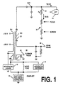
- FIGURE 1 is schematic diagram of a resistive divider circuit, according to the prior art, for generating focus voltage.
- FIGURE 2 is a schematic diagram of a peak detected circuit, according to the prior art, for generating focus voltage.
- FIGURE 3 is a schematic diagram of a circuit for generating focus voltage according to an inventive arrangement.
- FIGURE 4 is a schematic diagram of a focus screen assembly which can be used in the circuit of FIGURE 3.
- FIGURE 1 is a schematic diagram of a focus supply circuit embodying the prior art resistive divider network approach.
- Means 10 for generating a high voltage comprises a flyback transformer Tr1, having a primary winding W1 coupled to a horizontal driver circuit 12 and a horizontal deflection yoke.
- An East-West pincushion correction circuit 14 and horizontal centering circuit 16 are also included.
- a high voltage secondary winding W2 is used to generate a high voltage, or EHT, having a value of 30 KV, for example.
- the other end of the winding is coupled to a circuit which generates a beam sense signal for monitoring the beam current IBEAM level delivered to the cathode ray tube (CRT) 24.
- Another secondary winding W3 is a source of horizontal flyback pulses.
- Secondary winding W2 has an intermediate tap 22 identified, which is not used in the embodiment of FIGURE 1. The operation of means 10 is known in the art.
- Focus voltage and screen voltage for the cathode ray tube 24 are generated by a resistive chain 30, having an input terminal 32.
- the resistive chain 30 is coupled between the EHT voltage and ground.
- the resistive chain 30 is illustrated as three resistors; a fixed bias resistor R B and variable resistors for setting each of the focus and screen voltages.
- Resistor R B has a resistance of approximately 350 M Ohm and the resistance of the entire chain is approximately 500 M Ohm. This approach results in a useful bias current I BIAS , but exhibits a source impedance which is too high.
- FIGURE 2 is a schematic diagram of a focus supply circuit embodying the prior art peak detected approach. Means 10 for generating a high voltage is the same as explained in connection with FIGURE 1.
- a resistive chain 40 is coupled, through an input terminal 42, between the intermediate tap 22 of the winding W2 and ground. Resistive chain 40 is also illustrated as three resistors for purposes of simplicity. If tap 22 represents approximately one third ( 1 / 3 ) of a high voltage of 30 KV, for example, then a much smaller voltage drop is needed in the resistive divider to develop the focus and screen voltages than is the case in the circuit of FIGURE 1. Accordingly, the resistance of resistor R' B and the resistance of the entire chain 40 will also be lower than in resistive chain 30. This provides a lower source impedance, but a negligible bias current, which is not shown for that reason.
- FIGURE 3 is a schematic diagram of a focus supply circuit according to an inventive arrangement.
- Means 10 for generating a high voltage is the same as explained in connection with FIGURE 1.
- a resistive chain 50 has an input terminal 52, and is coupled between the EHT voltage and a ground 58.
- the ground of the resistive chain is denoted by a reference numeral for purposes of identifying resistive chain 50 in FIGURE 4, explained below.
- the resistive chain 50 also has a bias resistor RB having a value of approximately 350 M Ohm and the entire chain has a resistance of approximately 500 M Ohm.
- the circuit of FIGURE 3 also has an independent conductive path 26 between the tap 22 of winding W2 and an intermediate tap 54 of the resistive chain 50.
- the resulting topography represents a synergistic combination of the prior art approaches which, for the first time, provides a low source impedance and an adequate bias current I BIAS .
- the intermediate taps 22 and 54 be chosen so as to connect substantially equal voltage levels to one another.
- each intermediate tap is approximately a one third (1/3) tap, representing approximately 10 KV. It appears that differences between the intermediate tap voltages in a range of approximately ⁇ 5 % of the EHT can be tolerated without significantly compromising the advantages of the inventive arrangement.
- the low source impedance is achieved without increasing current density and substrate area in a focus screen assembly, as shown in FIGURE 4.
- the resistive chain 50 forms an integral part of a focus screen assembly 60, in which the resistors are formed by deposition on a ceramic substrate.
- Resistive chain 50 begins at input terminal 52, which is coupled to the EHT voltage.
- the other end of resistor chain 50 is coupled to focus ground at terminal 58.
- Resistor R B is shown, as are variable resistors for adjusting the focus voltages and screen voltage are also shown.
- the Focus 1 (horizontal) voltage is an output on terminal 56.
- the Focus 2 (vertical) voltage is an output on terminal 64.
- the Screen voltage is an output on terminal 66.
- Terminal 68 is an input for a dynamic focus correction signal.
- Focus screen assembly 60 differs from prior art focus screen assemblies in the provision of intermediate tap input 54, which is coupled between one terminal of resistor R B and the junction of resistors R X .
- EHT Operating Voltage
Landscapes
- Engineering & Computer Science (AREA)
- Multimedia (AREA)
- Signal Processing (AREA)
- Details Of Television Scanning (AREA)
- Coils Or Transformers For Communication (AREA)
- Transforming Electric Information Into Light Information (AREA)
- Vessels, Lead-In Wires, Accessory Apparatuses For Cathode-Ray Tubes (AREA)
- Dc-Dc Converters (AREA)
Description
- This invention relates to the field of developing focus supply voltages for cathode ray tubes in televisions and the like.
- A high voltage power supply, for example in a television receiver, generates a high voltage from the high voltage winding in a flyback transformer, sometimes constructed as an integrated high voltage transformer (IHVT). The voltage is boosted by a series of windings and diodes. The high voltage (HV), sometimes referred to as EHT (extra high tension) may be approximately 30 KV or higher, depending on the size of the cathode ray tube. Some receivers with larger tubes utilize high voltage boosters having a second transformer, a second horizontal output stage and a second high voltage winding. The horizontal focus voltage supply in a television receiver may be in the range of approximately one fifth (1/5) to one third (1/3) of the EHT. Focus voltage and screen voltage can therefore be derived from the EHT.
- A focus screen assembly is usually provided for generating the focus and screen voltages. The focus screen assembly, which is energized by the high voltage winding of the IHVT, includes a network of fixed resistors, variable resistors and capacitors. The assembly will generate horizontal focus voltage, also referred to as Focus 1 voltage, screen voltage and vertical focus voltage, also referred to as Focus 2 voltage. The component resistors of the assembly are deposited on a ceramic substrate and the assembly is fully enclosed and insulated. Means for adjusting the variable resistors to set the focus and screen voltage levels are accessible from outside the case. The assembly is coupled to the high voltage output of the IHVT, also referred to as the flyback transformer. The assembly utilizes a resistor chain to supply the focus and screen voltages at levels below the high voltage level.
- There are two approaches known for energizing a focus screen assembly, and appropriate focus screen assemblies are manufactured for each of these approaches. One approach is generally referred to as the resistor divider network approach. The other approach is generally referred to as the peak detected approach, although a resistor chain is also utilized in the focus screen assembly. The approaches differ in the point of the high voltage winding from which energy is coupled to the focus screen assembly.
- The resistor divider network approach, such as shown in FIGURE 1, energizes the focus screen assembly with the full value of the EHT, as supplied to the cathode ray tube. This approach tends to provide a rather large source impedance for the focus supply, for example approximately 170 MOhm, which can become a problem for focus leakage currents. Focus leakage currents can be caused by imperfections, impurities and gas particles in the tube. It will be appreciated that a leakage current of only 70 µamp, for example, will cause a large voltage drop against an impedance of 170 MOhm. One might try to reduce the source impedance of the resistive divider, but two problems in particular are encountered. Firstly, reducing the source impedance results in a higher current density, which requires a larger ceramic substrate area to handle the additional heat dissipation. This adds to the expense of the assembly. Secondly, it is costly in general to generate the high voltage in the first place. Energy loss through such heat dissipation is inefficient and costly, in and of itself. On the other hand, the resistive divider desirably provides a small bias current for the high voltage supply even when the cathode ray tube is not conducting. High voltage supply changes at low beam current levels are therefore reduced. As a consequence, raster size changes resulting from changes in beam current are minimized.
- The peak detected approach, such as shown in FIGURE 2, energizes the focus screen assembly from a tap of the high voltage winding of the IHVT. The voltage at the tap should be greater than the required focus voltage, so that an adjustment range is available. A one third (1/3) tap, that is, a voltage level equal to approximately one-third (1/3) of EHT, can be appropriate. This approach has the advantage of providing a lower source impedance, but disadvantageously, does not provide much preloading, in the form of a bias current for the high voltage supply. As a consequence, raster size changes resulting form changes in beam current are more likely. The problems associated with the peak detected approach are addressed in DE-A-33 18 503, which discloses a power supply for providing high voltages in a television set. A transformer has a secondary winding comprising at least two partial windings, which are coupled to a voltage multiplier to provide the high voltage. The high voltage is divided by a resistor divider to provide focus and grid voltages for the television set. A capacitor resonates with one of the partial windings to provide the power supply with a low source impedance. A junction of the resistor divider is coupled to the voltage multiplier circuit.
- The problem, then, is to provide a supply voltage for the focus screen assembly from a low impedance source, which minimizes voltage loss and dissipation, and at the same time, provide an adequate bias voltage for the high voltage supply, even when the cathode ray tube is not conducting.
- The problem can be solved in accordance with an inventive arrangement which combines the resistive divider approach and the peak detected approach. In a new approach, the resistor divider network is modified by connecting the tap on the IHVT, for example the one third (1/3) tap, to a tap of the same voltage as generated by the resistor chain in the focus screen assembly, for example, one third (1/3) of the EHT voltage. The source impedance is lower, resulting in higher efficiency and lower losses, thus securing the advantages of the peak detected approach. Moreover, an adequate bias current is provided for the high voltage supply even when the cathode ray tube is not conducting, thus securing the advantage of the resistive divider approach by minimizing raster size changes due to beam current variation.
- There is a concern regarding the consequences of not perfectly matching the voltage levels of the taps on the high voltage winding of the IHVT and the resistor chain respectively, for example, tapping 331/3 % of the high voltage winding and tapping 35 % of the voltage on the resistor chain. Such precise matching is not necessary, although close matching is desirable for maximum efficiency. There is a range of tolerance in the disparity between the tapped voltage levels in which the advantages of the inventive arrangement are fully realized. If the tap of the high voltage winding, for example, is 331/3 %, the tap voltage of the resistor chain can be in the range of approximately ± 5 % around the IHVT tap value with reasonably good results at the extremes.
- The invention is set out in the independent claims. Advantageous embodiments are set out in the dependent claims.
- FIGURE 1 is schematic diagram of a resistive divider circuit, according to the prior art, for generating focus voltage.
- FIGURE 2 is a schematic diagram of a peak detected circuit, according to the prior art, for generating focus voltage.
- FIGURE 3 is a schematic diagram of a circuit for generating focus voltage according to an inventive arrangement.
- FIGURE 4 is a schematic diagram of a focus screen assembly which can be used in the circuit of FIGURE 3.
- FIGURE 1 is a schematic diagram of a focus supply circuit embodying the prior art resistive divider network approach. Means 10 for generating a high voltage comprises a flyback transformer Tr1, having a primary winding W1 coupled to a
horizontal driver circuit 12 and a horizontal deflection yoke. An East-Westpincushion correction circuit 14 andhorizontal centering circuit 16 are also included. A high voltage secondary winding W2 is used to generate a high voltage, or EHT, having a value of 30 KV, for example. The other end of the winding is coupled to a circuit which generates a beam sense signal for monitoring the beam current IBEAM level delivered to the cathode ray tube (CRT) 24. Another secondary winding W3 is a source of horizontal flyback pulses. Secondary winding W2 has anintermediate tap 22 identified, which is not used in the embodiment of FIGURE 1. The operation ofmeans 10 is known in the art. - Focus voltage and screen voltage for the
cathode ray tube 24 are generated by aresistive chain 30, having aninput terminal 32. Theresistive chain 30 is coupled between the EHT voltage and ground. Theresistive chain 30 is illustrated as three resistors; a fixed bias resistor RB and variable resistors for setting each of the focus and screen voltages. When the resistive chain is itself embodied in a focus screen assembly, there are actually many more resistors than three. Resistor RB has a resistance of approximately 350 M Ohm and the resistance of the entire chain is approximately 500 M Ohm. This approach results in a useful bias current IBIAS, but exhibits a source impedance which is too high. - FIGURE 2 is a schematic diagram of a focus supply circuit embodying the prior art peak detected approach. Means 10 for generating a high voltage is the same as explained in connection with FIGURE 1. In FIGURE 2, a
resistive chain 40 is coupled, through aninput terminal 42, between theintermediate tap 22 of the winding W2 and ground.Resistive chain 40 is also illustrated as three resistors for purposes of simplicity. Iftap 22 represents approximately one third (1/3) of a high voltage of 30 KV, for example, then a much smaller voltage drop is needed in the resistive divider to develop the focus and screen voltages than is the case in the circuit of FIGURE 1. Accordingly, the resistance of resistor R'B and the resistance of theentire chain 40 will also be lower than inresistive chain 30. This provides a lower source impedance, but a negligible bias current, which is not shown for that reason. - FIGURE 3 is a schematic diagram of a focus supply circuit according to an inventive arrangement. Means 10 for generating a high voltage is the same as explained in connection with FIGURE 1. A
resistive chain 50 has aninput terminal 52, and is coupled between the EHT voltage and aground 58. The ground of the resistive chain is denoted by a reference numeral for purposes of identifyingresistive chain 50 in FIGURE 4, explained below. Theresistive chain 50 also has a bias resistor RB having a value of approximately 350 M Ohm and the entire chain has a resistance of approximately 500 M Ohm. - The circuit of FIGURE 3 also has an independent
conductive path 26 between thetap 22 of winding W2 and anintermediate tap 54 of theresistive chain 50. The resulting topography represents a synergistic combination of the prior art approaches which, for the first time, provides a low source impedance and an adequate bias current IBIAS. It is preferable that the intermediate taps 22 and 54 be chosen so as to connect substantially equal voltage levels to one another. In the illustrated embodiment, each intermediate tap is approximately a one third (1/3) tap, representing approximately 10 KV. It appears that differences between the intermediate tap voltages in a range of approximately ± 5 % of the EHT can be tolerated without significantly compromising the advantages of the inventive arrangement. Moreover, the low source impedance is achieved without increasing current density and substrate area in a focus screen assembly, as shown in FIGURE 4. - With reference to FIGURE 4, the
resistive chain 50 forms an integral part of afocus screen assembly 60, in which the resistors are formed by deposition on a ceramic substrate.Resistive chain 50 begins atinput terminal 52, which is coupled to the EHT voltage. The other end ofresistor chain 50 is coupled to focus ground atterminal 58. Resistor RB is shown, as are variable resistors for adjusting the focus voltages and screen voltage are also shown. The Focus 1 (horizontal) voltage is an output onterminal 56. The Focus 2 (vertical) voltage is an output onterminal 64. The Screen voltage is an output onterminal 66.Terminal 68 is an input for a dynamic focus correction signal.Focus screen assembly 60 differs from prior art focus screen assemblies in the provision ofintermediate tap input 54, which is coupled between one terminal of resistor RB and the junction of resistors RX. - The present specifications for the
focus screen assembly 60 as it will be used in the CTC-189 chassis manufactured by Thomson Consumer Electronics, Inc., which are not already shown on the drawing, are as follows:Operating Voltage (EHT) 30.0 KV - 34.5 KV; Maximum DC Voltage 35.5 KV; Resistance Total EHT IN to Terminal 62290 M Ohm ±20 %; Resistance Focus Total 500 M Ohm Nominal; Resistance Bleeder Total (R2 + R3) 700 M Ohm Nominal; Focus 1 + Focus 2 Maximum ≥ 33 % of EHT; Focus 1 + Focus 2 Minimum ≤ 28 % of EHT; Screen Maximum ≥ 485 V; Screen Minimum ≤ 135 V; and, IHVT Tap Voltage Range 35 % - 37 % of EHT.
Claims (6)
- A circuit, comprising:characterized by:means (10) for generating a high voltage (EHT) for energizing a cathode ray tube (24), including a transformer (Tr1) having a high voltage winding (W2) with at least one intermediate output tap (22); and,a resistive chain (50) with an input terminal (52) coupled for receiving said high voltage (EHT), a focus output terminal (FOCUS) for energizing a focus electrode of said cathode ray tube and at least one intermediate input tap (54) between said input terminal and said focus output terminal, coupled to said at least one intermediate tap (22) of said high voltage winding (W2) by a conduction path (26);
said intermediate output tap (22) and said intermediate input tap (54) each having a voltage level, established independently of said conduction path, which is equal to a voltage level of said focus output terminal ± approximately five percent (5 %) of said high voltage. - The circuit of claim 1, characterized in that said resistive chain (50) is part of a focus screen assembly (60).
- The circuit of claim 1, characterized in that said at least one intermediate output tap (22) of said high voltage winding (W2) provides an intermediate output voltage of approximately one third (1/3) of said high voltage (EHT), ± approximately five percent (5 %), and said intermediate input tap (54) of said resistive chain (50) corresponds to a voltage level in the range of approximately said one third (1/3) of said high voltage (EHT), ± approximately five percent (5 %).
- A circuit, comprising:characterized in thatmeans (10) for generating voltage (EHT) at a high voltage level for energizing a cathode ray tube (24), including a transformer (Tr1) having a high voltage winding (W2) with at least one intermediate transformer tap (22) having a first tap voltage level;a resistive chain (50) with an input terminal (52) coupled for receiving said high voltage (EHT), said resistive chain (50) providing a conductive path for a bias current for said cathode ray tube (24) through said input terminal (52), said resistive chain (50) having a focus output terminal (FOCUS) for energizing a focus electrode of said cathode ray tube at a focus voltage level, said focus electrode tending to be a source of a leakage current through said focus output terminal (FOCUS); andat least one intermediate resistive chain tap (54) between said input terminal (52) and said focus output terminal (FOCUS), said at least one intermediate resistive chain tap (54) having a second tap voltage established by said resistive chain (50) and being coupled to said at least one intermediate transformer tap (22) by a conduction path (26);
said first and second tap voltage levels correspond to one another and are equal to said focus voltage level ± approximately five percent (5 %) of said high voltage level, said conductive path (26) presenting a sufficiently low impedance to said focus output terminal (FOCUS) to substantially prevent variation of said high voltage (EHT) due to variation of said leakage current. - The focus supply circuit of claim 4, characterized in that said at least one intermediate output tap (22) of said high voltage winding (W2) provides an intermediate output voltage of approximately one third (1/3) of said high voltage (EHT), ± approximately five percent (5 %), and said intermediate input tap (54) of said resistive chain (50) corresponds to a voltage level in the range of approximately said one third (1/3) of said high voltage (EHT), ± approximately five percent (5 %).
- The circuit of claim 5, characterized in that said resistive chain (50) is part of a focus screen assembly (60).
Applications Claiming Priority (2)
| Application Number | Priority Date | Filing Date | Title |
|---|---|---|---|
| US08/285,329 US5602447A (en) | 1994-08-03 | 1994-08-03 | Cathode ray tube focus supply |
| US285329 | 1994-08-03 |
Publications (3)
| Publication Number | Publication Date |
|---|---|
| EP0696134A2 EP0696134A2 (en) | 1996-02-07 |
| EP0696134A3 EP0696134A3 (en) | 1996-05-01 |
| EP0696134B1 true EP0696134B1 (en) | 2000-05-03 |
Family
ID=23093762
Family Applications (1)
| Application Number | Title | Priority Date | Filing Date |
|---|---|---|---|
| EP95111561A Revoked EP0696134B1 (en) | 1994-08-03 | 1995-07-22 | Cathode ray tube focus supply |
Country Status (9)
| Country | Link |
|---|---|
| US (1) | US5602447A (en) |
| EP (1) | EP0696134B1 (en) |
| JP (1) | JPH0870389A (en) |
| KR (1) | KR100383748B1 (en) |
| CN (1) | CN1123208C (en) |
| DE (1) | DE69516597T2 (en) |
| MY (1) | MY112162A (en) |
| SG (1) | SG50351A1 (en) |
| TW (1) | TW293133B (en) |
Families Citing this family (6)
| Publication number | Priority date | Publication date | Assignee | Title |
|---|---|---|---|---|
| DE19718656A1 (en) * | 1997-05-02 | 1998-11-05 | Philips Patentverwaltung | High voltage generator with a high voltage unit |
| US5982641A (en) * | 1998-08-07 | 1999-11-09 | Thomson Consumer Electronics, Inc. | High-voltage power supply for video display apparatus |
| US6009006A (en) * | 1998-08-07 | 1999-12-28 | Thomson Consumer Electronics, Inc. | Synchronized high voltage generator |
| KR20020019774A (en) * | 2000-09-07 | 2002-03-13 | 김대철 | Dynamic focus circuit for computer monitor using current type transformer |
| KR100406572B1 (en) * | 2001-05-04 | 2003-11-20 | 삼성전자주식회사 | power supplying device for electron gun in CDT |
| AU2003262401A1 (en) * | 2002-04-19 | 2003-11-03 | Thomson Licensing S.A. | Passive compensation of focus tracking utilizing winding and capacitor |
Family Cites Families (4)
| Publication number | Priority date | Publication date | Assignee | Title |
|---|---|---|---|---|
| GB1409580A (en) * | 1971-12-23 | 1975-10-08 | Matsushita Electric Industrial Co Ltd | Cathode-ray tube driving circuit |
| JPS59172945A (en) * | 1983-03-22 | 1984-09-29 | Victor Co Of Japan Ltd | Dc high voltage generator |
| DE3318503C2 (en) * | 1983-05-20 | 1986-03-06 | Ernst Roederstein Spezialfabrik für Kondensatoren GmbH, 8300 Landshut | Generator for high voltage generation |
| JPH01126167A (en) * | 1987-11-10 | 1989-05-18 | Sanyo Electric Co Ltd | Flyback transformer |
-
1994
- 1994-08-03 US US08/285,329 patent/US5602447A/en not_active Expired - Fee Related
- 1994-08-04 TW TW083107149A patent/TW293133B/zh active
-
1995
- 1995-07-22 DE DE69516597T patent/DE69516597T2/en not_active Revoked
- 1995-07-22 EP EP95111561A patent/EP0696134B1/en not_active Revoked
- 1995-07-31 MY MYPI95002216A patent/MY112162A/en unknown
- 1995-07-31 KR KR1019950023310A patent/KR100383748B1/en not_active Expired - Fee Related
- 1995-07-31 SG SG1995000991A patent/SG50351A1/en unknown
- 1995-08-02 JP JP7226923A patent/JPH0870389A/en active Pending
- 1995-08-02 CN CN95109509A patent/CN1123208C/en not_active Expired - Fee Related
Also Published As
| Publication number | Publication date |
|---|---|
| SG50351A1 (en) | 1998-07-20 |
| JPH0870389A (en) | 1996-03-12 |
| CN1116795A (en) | 1996-02-14 |
| KR960009594A (en) | 1996-03-22 |
| DE69516597D1 (en) | 2000-06-08 |
| EP0696134A2 (en) | 1996-02-07 |
| MY112162A (en) | 2001-04-30 |
| KR100383748B1 (en) | 2003-07-07 |
| DE69516597T2 (en) | 2000-09-07 |
| EP0696134A3 (en) | 1996-05-01 |
| CN1123208C (en) | 2003-10-01 |
| TW293133B (en) | 1996-12-11 |
| US5602447A (en) | 1997-02-11 |
Similar Documents
| Publication | Publication Date | Title |
|---|---|---|
| US5130615A (en) | Television apparatus having kinescope spot burn protection circuit with extended grid cut-off time constant | |
| US5602447A (en) | Cathode ray tube focus supply | |
| JP3571086B2 (en) | Power supply for television equipment | |
| US5394067A (en) | Regulated high DC voltage supply | |
| US5614789A (en) | Apparatus and method of reducing varying electrical fields in video display terminals | |
| US4835668A (en) | Power supply with two output voltages | |
| US5677730A (en) | Spot elimination circuit for a cathode ray tube | |
| US3798497A (en) | Solid-state television receiver with magnetically regulated power supply | |
| US4187451A (en) | Color picture display device with a circuit for generating a screen grid voltage | |
| US3691422A (en) | Circuit arrangement for generating a sawtooth current in a line deflection coil for a display tube conveying a beam current and for generating an eht | |
| CA2039784C (en) | Power supply for an electrode of a crt | |
| JP3370856B2 (en) | Dynamic focus correction circuit | |
| US6369528B1 (en) | Vertical deflection circuit | |
| CA2164784C (en) | Electromagnetic focusing circuit for cathode-ray tube | |
| US5703443A (en) | Horizontal deflection output circuit | |
| US6049180A (en) | High voltage regulated supply particularly suited for visual displays | |
| CN100413313C (en) | Focus Voltage Amplifier | |
| US6661188B2 (en) | Cathode ray tube filament voltage control with a multifrequency deflection scanner | |
| JPH0221716B2 (en) | ||
| JP3313181B2 (en) | High voltage output stop circuit | |
| JPH0318791B2 (en) | ||
| JPH04348668A (en) | Spot killer circuit | |
| US20040075403A1 (en) | High voltage supply for a picture tube | |
| EP0114430A1 (en) | Picture display device comprising a power supply circuit and a line deflection circuit | |
| MXPA04010329A (en) | Focus voltage control arrangement. |
Legal Events
| Date | Code | Title | Description |
|---|---|---|---|
| PUAI | Public reference made under article 153(3) epc to a published international application that has entered the european phase |
Free format text: ORIGINAL CODE: 0009012 |
|
| AK | Designated contracting states |
Kind code of ref document: A2 Designated state(s): DE GB |
|
| PUAL | Search report despatched |
Free format text: ORIGINAL CODE: 0009013 |
|
| AK | Designated contracting states |
Kind code of ref document: A3 Designated state(s): DE GB |
|
| 17P | Request for examination filed |
Effective date: 19960626 |
|
| 17Q | First examination report despatched |
Effective date: 19980715 |
|
| GRAG | Despatch of communication of intention to grant |
Free format text: ORIGINAL CODE: EPIDOS AGRA |
|
| GRAG | Despatch of communication of intention to grant |
Free format text: ORIGINAL CODE: EPIDOS AGRA |
|
| GRAH | Despatch of communication of intention to grant a patent |
Free format text: ORIGINAL CODE: EPIDOS IGRA |
|
| GRAH | Despatch of communication of intention to grant a patent |
Free format text: ORIGINAL CODE: EPIDOS IGRA |
|
| GRAA | (expected) grant |
Free format text: ORIGINAL CODE: 0009210 |
|
| AK | Designated contracting states |
Kind code of ref document: B1 Designated state(s): DE GB |
|
| REF | Corresponds to: |
Ref document number: 69516597 Country of ref document: DE Date of ref document: 20000608 |
|
| EN | Fr: translation not filed | ||
| PLBQ | Unpublished change to opponent data |
Free format text: ORIGINAL CODE: EPIDOS OPPO |
|
| PLBI | Opposition filed |
Free format text: ORIGINAL CODE: 0009260 |
|
| PLBF | Reply of patent proprietor to notice(s) of opposition |
Free format text: ORIGINAL CODE: EPIDOS OBSO |
|
| 26 | Opposition filed |
Opponent name: INTERESSENGEMEINSCHAFT FUER RUNDFUNKSCHUTZRECHTE G Effective date: 20010130 |
|
| PLBF | Reply of patent proprietor to notice(s) of opposition |
Free format text: ORIGINAL CODE: EPIDOS OBSO |
|
| PLBF | Reply of patent proprietor to notice(s) of opposition |
Free format text: ORIGINAL CODE: EPIDOS OBSO |
|
| REG | Reference to a national code |
Ref country code: GB Ref legal event code: IF02 |
|
| REG | Reference to a national code |
Ref country code: GB Ref legal event code: 746 Effective date: 20030103 |
|
| PGFP | Annual fee paid to national office [announced via postgrant information from national office to epo] |
Ref country code: GB Payment date: 20030609 Year of fee payment: 9 |
|
| PGFP | Annual fee paid to national office [announced via postgrant information from national office to epo] |
Ref country code: DE Payment date: 20030707 Year of fee payment: 9 |
|
| RDAF | Communication despatched that patent is revoked |
Free format text: ORIGINAL CODE: EPIDOSNREV1 |
|
| PLCK | Communication despatched that opposition was rejected |
Free format text: ORIGINAL CODE: EPIDOSNREJ1 |
|
| PLAO | Information deleted related to despatch of communication that opposition is rejected |
Free format text: ORIGINAL CODE: EPIDOSDREJ1 |
|
| RDAF | Communication despatched that patent is revoked |
Free format text: ORIGINAL CODE: EPIDOSNREV1 |
|
| RDAG | Patent revoked |
Free format text: ORIGINAL CODE: 0009271 |
|
| STAA | Information on the status of an ep patent application or granted ep patent |
Free format text: STATUS: PATENT REVOKED |
|
| 27W | Patent revoked |
Effective date: 20031120 |
|
| GBPR | Gb: patent revoked under art. 102 of the ep convention designating the uk as contracting state |
Free format text: 20031120 |