EP0696130A2 - A system and method for implementing fast high addressability error diffusion process - Google Patents
A system and method for implementing fast high addressability error diffusion process Download PDFInfo
- Publication number
- EP0696130A2 EP0696130A2 EP95305325A EP95305325A EP0696130A2 EP 0696130 A2 EP0696130 A2 EP 0696130A2 EP 95305325 A EP95305325 A EP 95305325A EP 95305325 A EP95305325 A EP 95305325A EP 0696130 A2 EP0696130 A2 EP 0696130A2
- Authority
- EP
- European Patent Office
- Prior art keywords
- error
- grey level
- value
- threshold
- resolution
- Prior art date
- Legal status (The legal status is an assumption and is not a legal conclusion. Google has not performed a legal analysis and makes no representation as to the accuracy of the status listed.)
- Granted
Links
Images


Classifications
-
- H—ELECTRICITY
- H04—ELECTRIC COMMUNICATION TECHNIQUE
- H04N—PICTORIAL COMMUNICATION, e.g. TELEVISION
- H04N1/00—Scanning, transmission or reproduction of documents or the like, e.g. facsimile transmission; Details thereof
- H04N1/40—Picture signal circuits
- H04N1/405—Halftoning, i.e. converting the picture signal of a continuous-tone original into a corresponding signal showing only two levels
- H04N1/4051—Halftoning, i.e. converting the picture signal of a continuous-tone original into a corresponding signal showing only two levels producing a dispersed dots halftone pattern, the dots having substantially the same size
- H04N1/4052—Halftoning, i.e. converting the picture signal of a continuous-tone original into a corresponding signal showing only two levels producing a dispersed dots halftone pattern, the dots having substantially the same size by error diffusion, i.e. transferring the binarising error to neighbouring dot decisions
- H04N1/4053—Halftoning, i.e. converting the picture signal of a continuous-tone original into a corresponding signal showing only two levels producing a dispersed dots halftone pattern, the dots having substantially the same size by error diffusion, i.e. transferring the binarising error to neighbouring dot decisions with threshold modulated relative to input image data or vice versa
Definitions
- the present invention is directed to the architecture of an error diffusion process. More specifically, the present invention is related to the architecture of a high addressability error diffusion process which allows the reduction of a multi-level grey signal to be carried out in the time constraints of an image rendering system.
- Error diffusion is a well known method of processing grey scale images on a binary output device.
- One of the key ingredients in error diffusion is a requirement to propagate or diffuse the error which is generated by reducing (binarizing) the grey level value of a grey scale image.
- the input grey level at pixel location i and pixel location i + 1 is represented by V i and V i+1 , respectively.
- the pixel values are assumed to be 8 bit integers wherein, for the sake of explanation, 0 denotes white and 255 denotes black.
- the rendering error, at a resolution lower than the addressability resolution, that passes from upstream pixels to the downstream pixel location is denoted by e i .
- a feature of high addressability involves interpolation between pixels, the creation of subpixels. This interpolation impacts the high addressability error diffusion process. More specifically, depending on the way the interpolation is done, distinct outputs can be obtained utilizing a high addressability error diffusion process.
- One such method of interpolation is as follows.
- Figures 1-7 illustrate the computational steps required to perform high addressability error diffusion using a particular interpolation scheme.
- the pixel value V i and V i+1 are obtained.
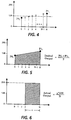
- the actual pixel values are graphically illustrated in Figure 1, wherein the pixel value V i represents the pixel value at the subpixel position 0 and the pixel value V i+1 represents the pixel value at the N-1 subpixel.
- the pixel values range from 0 to 255 utilizing a conventional eight bit dataword to represent the multi-level grey value of the image data to be process. It is noted that any range can be utilized to represent the grey level value of the image data; for example, 0 to 511, 0 to 127, etc.
- a diffused error component e i (the accumulated error from previous pixel binarization processes) is added to the pixel values V i and V i+1 .
- the error component e i consists of two components, e FIFO and e FB , where e FIFO is the summed error component stored in a line buffer and e FB is the feedback error component.
- the adding of the error component e i is illustrated graphically in Figure 2.
- the interpolated subpixel values are computed, as illustrated in Figure 3.
- each interpolated subpixel value is compared to a threshold level.
- the threshold value is 128. It is noted that this threshold value can be any value within the range of the image data depending upon the desired results.
- each subpixel which has a value greater than or equal to 128 is set ON.
- the desired output (P0 i + P1 i )/2 is computed.
- This computing of the desired output is graphically illustrated in Figure 5.
- the actual output is computed.
- the actual output is equal to n*255/N where n is the number of subpixels that have been turned ON as the result of the comparison illustrated in Figure 4.
- a graphical representation of the computed actual output is shown in Figure 6.
- the error diffusion method computes the error to be propagated downstream. This error is computed as the desired output minus the actual output. A graphical representation of this computation is shown in Figure 7.
- the error e i+1 represents the error from the present binarization process.
- the error from the binarization process is distributed to downstream pixels.
- the distributing of the error e i +1 to downstream pixels is illustrated in Figure 8.
- the distribution of error utilizes a set of error diffusion coefficients which allow fast processing by simple bit shifting.
- Figure 8 illustrates the coefficients associated with each pixel location. An example of the exact coefficients are discussed in U.S. Patent Application, Serial No. 08/167,758.
- a first aspect of the present invention is a method of diffusing error generated from thresholding a grey level value representing a pixel.
- the method receives the grey level value representing the pixel wherein the grey level value has a first resolution.
- the grey level value is converted to a second resolution, the second resolution being higher than the first resolution.
- the converted grey value is then thresholded.
- a plurality of possible error values are generated in parallel with the conversion and thresholding steps. One of the plurality of possible error values is selected based on a number of subpixels exceeding a threshold value.
- the selected error value is diffused to grey level values representing adjacent pixels.
- step (b) further comprises the substep of: (b3) computing a plurality of subpixel grey level values B n , the subpixel grey level values B n being equal to P0 + n(P1-P0)/N, wherein n is equal to 0 to N-1, P0 is equal to the first grey level value, P1 is equal to the second grey value, and N is equal to a high addressability characteristic.
- (d) comprises the substeps of: (d1) calculating a desired output;(d2) calculating a plurality of possible actual outputs; and (d3) calculating the plurality of possible error values, each error value being equal to the desired output minus a possible actual output.
- the method preferably further comprises the step of: (g) screening the grey level value with a predetermined screen prior to the execution of said step (b).
- a second aspect of the present invention is a system for diffusing error generated from threshold a grey level value representing a pixel.
- This system includes input means for receiving the grey level value representing the pixel, the grey level value having a first resolution and high addressability means for converting the grey level value to a second resolution, the second resolution being higher than the first resolution.
- Threshold means thresholds the converted grey level value, and error means generates a plurality of possible error values in parallel with the conversion and thresholding means.
- Selection means selects one of the plurality of possible error values based on a number of subpixels exceeding a threshold value.
- Error diffusing means diffuses the selected error value to grey level values representing adjacent pixels.
- the high addressability means further computes a plurality of subpixel grey values B n , the subpixel grey level values B n being equal to P0 + n(P1-P0)/N, wherein n is equal to 0 to N-1, P0 is equal to the first grey level value, P1 is equal to the second grey level value, and N is equal to a high addressability characteristic.
- said error means comprises: first means for calculating a desired output; second means for calculating a plurality of possible actual outputs; and third means for calculating the plurality of possible error values, each possible error value being equal to the desired output minus a possible actual output.
- the system preferably further comprises: screening means for screening the grey level value with a predetermined screen prior to conversion by said conversion means.
- a third aspect of the present invention is a method of generating an error from a threshold process.
- the method thresholds a grey level value of a pixel.
- a plurality of possible error values are generated in parallel with the thresholding step.
- One of the plurality of possible error values is selected based on a number of subpixels exceeding a threshold value.
- a fourth aspect of the present invention is a system for generating an error from a threshold process.
- the system includes threshold means for thresholding a grey level value of a pixel and error means for generating a plurality of possible error values are generated in parallel with the thresholding means.
- Selection means selects one of the plurality of possible error values based on a number of subpixels exceeding a threshold value.
- a fifth aspect of the present invention is a binary printing system for rendering marks on a receiving medium.
- the binary printing system includes input means for receiving a grey level signal corresponding to a pixel and having a first resolution.
- Interpolation means converts the grey level signal to a second resolution which is higher than the first resolution.
- Binarization means binarizes the converted grey level signal so as to output a binary signal.
- Error means generates a plurality of possible error values in parallel with the interpolation and binarization means.
- Selection means selects one of the plurality of possible error values based on a number of subpixels exceeding a threshold value.
- Diffusing means diffuses the selected error value to grey level signals corresponding to pixels adjacent to the binarized pixel.
- rendering means converts the binary signal into a mark on the receiving medium.
- the hardware implementation of the high addressability error diffusion must meet the time restraints of the throughput specifications of the image rendering device utilizing the high addressability error diffusion method. More specifically, to be implemented in present day image rendering devices, the error computation must be completed in one clock cycle, since half of the error is diffused to the next pixel in the fast scan direction. The error which is diffused downward in the slow scan direction is summed and stored in a buffer. This portion of the error is part of the distributed error component required for binarizing pixels on the next scanline. This summing, however, can be performed several cycles later, since this error component is not needed until the following scanline.
- the input video signal is split and latched in latch 101 so as to produce the pixel value V0 i and V1 i .
- V0 i represents the latched input video signal V1 i , in other words, V0 i represents the pixel value just proceeding the pixel value V1 i in the same same scanline.
- the pixel value V0 i is fed into an adder 103 with the error component e i .
- the error component e i is fed into an adder 105 along with the input video signal V1 i .
- the adder 103 produces an output signal P0 i which is fed into a 2-complements circuit 107 to produce negative P0 i .
- Negative P0 i is fed into an adder 109 along with the value P1 i to produce the value of P1 i -P0 i .
- Negative P0 i is also fed into adder 111 which is summed with the threshold value.
- the threshold value is 128.
- the sum from adder 111 is fed into multiplier 115 so that the value (128 - P0 i ) can be multiplied by the high addressability characteristic value N.
- the resulting product is then divided by the sum from adder 109 by a divider circuit 117.
- the resulting quotient is represented by n and fed into a decoder 119.
- the actual function of decoder 119 is graphically illustrated in Figure 10.
- the decoder 119 determines the intersection of the P0 i /P1 i line and the value 128. From the determination of this intersection, the decoder 119 determines the number of subpixels n which are turned ON. The results from decoder 119 are fed as binarized output to a print engine and also to a multiplier 121. Multiplier 121 multiplies the output from decoder 119 with the value (-255/N). The product of multiplier 121 is added to a sum generated by an adder 113 in adder 123. Adder 113 adds the values P0 i and P1 i to produce the value P1 i + P0 i .
- the results of adder 123 represents the error component e i+1 which is fed into a simple bit shifting circuit 125 to produce various error values that will be utilized in the distribution process.
- the error values generated by the bit shifting circuit 125 are fed into an error distribution circuit 127, wherein half the error Err B is distributed to the next pixel in the same scanline and the other half of the error Err A is distributed to various pixels in the next scanline according to the weighting coefficients established in the error distribution circuit 127.
- this hardware implementation of the high addressability error diffusion assumes that there are no time constraints, that there are no system's throughput specification requiring clock cycles exceeding 50 megahertz, or that the system has a microprocessor capable of operating at an instruction per second rate greater than 100 Mips (million instructions per second).
- typical image rendering devices have clock cycles which exceed 50 megahertz and require all image processing of a single pixel to be completed within approximately 20 nanoseconds of time to operate in realtime; i.e., within the throughput specifications of mid-volume to high volume printing systems.
- the present invention decomposes the computation of the high addressability error diffusion method into two categories.
- the first category includes all computations which can be performed on the interpolated video signal including all possible subpixel error calculations outside or prior to entering a feedback path, and the second category is calculations which include the remaining computations that must be performed within one clock cycle (i.e., inside the feedback path).
- the diffused error value is broken into two components, one component being the sum error which is stored and readily available in the FIFO buffer, namely e FIFO , and the other is the fast scan feedback error component, e FB , passed from binarizing of the neighbor pixel immediately preceding the pixel being processed in the fast scan direction.
- Figures 11-14 represent the computations which can be performed prior to entering the feedback loop
- Figures 15-19 are the computations which are performed within one clock cycle or within the feedback loop.
- some of these computations are performed in parallel. The parallel computations will be discussed with respect to Figures 11-19.
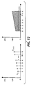
- Figure 11 illustrates two such parallel computations which are carried out in the present invention. More specifically, Figure 11 illustrates that the pixel values V i and V i+1 are obtained in parallel to the beginning of the computation of the desired output for a single subpixel wherein the desired output is computed without including the diffused error components e FIFO or e FB .
- the preferred embodiment of the present invention computes the interpolated subpixel values in the same way as illustrated in Figure 3. However, in parallel with this computation of the interpolated subpixel values, the desired output is continued to be computed by adding the error component e FIFO . This, is graphically represented in Figure 12.
- the error component e FIFO is added to the pixel values V i , and V i+1 and the interpolated subpixels as illustrated in Figure 13.
- all possible actual subpixel outputs are subtracted from the desired output without including the diffused error component e FB .
- N possible actual subpixel outputs are subtracted from the desired output computed in Figure 12 to produce N possible error outputs e p (the desired output minus the actual output is equal to the error e p ).
- the computations illustrated in Figure 13 are carried out in parallel with the computations illustrated in Figure 14. It is further noted that the computations illustrated in Figures 11-14 are implemented outside the feedback loop.
- the computations are illustrated by Figures 15-19.
- the error component e FB is added to the pixel values V i , V i+1 , and the various interpolated subpixel values as illustrated in Figure 15.
- the error component e FB is added to all possible subpixel desired outputs as illustrated in Figure 16.
- the error component e FB is individually added to all N error results (e p ) stemming from the calculations illustrated by Figure 14.
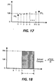
- each interpolated subpixel value is compared to a threshold value of 128, and the subpixels having a value greater than or equal to the threshold value are turned ON.
- This process is graphically illustrated in Figure 17 and 18 wherein Figure 17 shows the comparison of the interpolated subpixel values with the threshold values, and Figure 18 shows the turning ON of the subpixels which have a value greater than or equal to the threshold value.
- Figure 19 illustrates the properly selected error value from the various simultaneously available error values produced by the computations illustrated in Figure 16.
- the selected error value is then distributed to downstream pixels utilizing any conventional error diffusion technique.
- the error is distributed to downstream pixels utilizing the error diffusion coefficients discussed above.
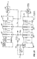
- Figure 20 illustrates a functional block diagram of the parallel pipeline high addressability error diffusion circuit of the preferred embodiment of the present invention.
- the input video signal is fed into an error calculation circuit 1 and a video modification circuit 3.
- the error components e FIFO (Err B ) and e FB (Err A ) are also fed into the error calculation circuit 1.
- the error calculation circuit calculates all the various possible error values that can result from the presently occurring binarization process.
- the selection of the proper error to be output by the error calculation circuit 1 is based upon the received error selection signal which will be discussed in more detail below.
- the selected error value from the error calculation circuit 1 is fed into a coefficient matrix circuit 5 which distributes the error based upon a set of weighting coefficients.
- the coefficient matrix circuit 5 splits the error values into the two components e FIFO (Err B ) and e FB (Err A ).
- the feedback error, Err A is fed back to the video modification circuit 3 and the error calculation circuit 1 from the coefficient matrix circuit 5.
- the video modification circuit 3 also receives the Err B from buffer 9.
- the video modification circuit 3 produces the interpolated subpixel values for the high addressability error diffusion method wherein the interpolated subpixel values are fed into the binarization circuit 7 along with a threshold value.
- the threshold value is 128. However, it is noted that this threshold value can be any value.
- the binarization circuit 7 binarizes the inputted video data so as to output binarized image data for the utilization by an image rendering device.
- the binarization circuit 7 also produces the error selection signal which is utilized by the error calculation circuit 1 to choose the correct error value to be fed to the coefficient matrix circuit 5.
- This error selection signal represents the number of interpolated subpixels which are turned ON during the binarization process.
- the error calculation circuit 1 may include a multiplexer to make this selection.
- the error calculation circuit 1 is in parallel with the video modification circuit and the binarization circuit.
- the high addressability error diffusion architecture of the present invention is implemented on an ASIC, thereby enabling hardware implementation so that the image data can be binarized within the time constraints and throughput specifications of a high speed image rendering device.
- Figure 21 illustrates a detail block diagram of the circuit of the preferred embodiment of the present invention. As illustrated in Figure 21, many of the computations, as previously described with respect to Figures 11-19, are carried out in parallel.
- Pixel values V i and V i+1 are obtained by the utilization of a latch 205 which latches the video signal so that two adjacent fast scan pixels are available for processing.
- the pixel values V i and V i+1 are summed in adder 206 and the sum is divided in half by divider 207.
- the result from divider 207 is fed into adder 208 with the error term e FIFO .
- the sum represents the desired output to the printer.
- an actual output generation circuit 200 produces all possible outputs to the printer based on the high addressability characteristic. It is noted that these values are negative since an adder is used for substraction operations. If the high addressability characteristic is N, N possible actual outputs will be generated. Also in parallel to the above described process, a subpixel circuit generated all the interpolated subpixels based on the pixel values V i and V i+1 .
- the error component e FIFO is added to each of the interpolated subpixels by adder 210.
- each possible actual outputs (negative values) is individually added to the desired output by adder 201.
- N possible actual subpixel outputs are subtracted from the desired output to produce N possible error outputs.
- a feedback error term e FB is added to each summation from adders 210 and 201, respectively. These computations are carried out in parallel. After completing these parallel computations, each interpolated subpixel from adder 211 is compared to a threshold value in threshold circuit 212. The subpixels having a value greater than or equal to the threshold value are turned ON. Threshold circuit outputs a number representing the number of sub pixels turned ON. This information is fed into a decode logic circuit which produces a binary therefrom to be sent to a printer.
- the error terms from adder 202 are fed into a multiplexer 203 which chooses which error term to propagate to down stream pixels.
- the error term is selected based on a control signal received from the decode logic circuit 213.
- the selected error term is fed into a distribution circuit 204 which produces the next feedback error and the error to be stored in a buffer for utilization in the processing of the next scanline.
- the present invention is also applicable to an image processing system which combines screening with high addressability error diffusion.
- a full description of the screening and high addressability error diffusion process is disclosed in EP-A-000,000, corresponding to U.S. Patent Application, Serial Number 08/285,328, filed concurrently herewith.
- the terms pixel and subpixel have been utilized. These terms may refer to an electrical (or optical, if fiber optics are used) signal which represent the physically measureable optical properties at a physically definable area on a receiving medium.
- the receiving medium can be any tangible document, photoreceptor, or marking material transfer medium.
- the terms pixel and subpixel may refer to an electrical (or optical, if fiber optics are used) signal which represent the physically measureable optical properties at a physically definable area on a display medium.
- a plurality of the physically definable areas for both situations represent the physically measureable optical properties of the entire physical image to be rendered by either a material marking device, electrical or magnetic marking device, or optical display device.
- pixel may refer to an electrical (or optical, if fiber optics are used) signal which represents physical optical property data generated from a single photosensor cell when scanning a physical image so as to convert the physical optical properties of the physical image to an electronic or electrical representation.
- a pixel is an electrical (or optical) representation of the physical optical properties of a physical image measured at a physically definable area on an optical sensor.
- the present invention has been described with respect to a video range of 0 to 255.
- the video range can be any suitable range to describe the grey level of the pixel being processed.
- the present invention is readily applicable to any rendering system, not necessarily a binary output device. It is contemplated that the concepts of the present invention are readily applicable to a four level output terminal or higher.
- the present invention has been described with respect to a monochrome or black/white environment.
- the concepts of the present invention are readily applicable to a color environment. Namely, the high addressability error diffusion architecture of the present invention can be replicate three times and placed in parallel to each other so that each color space value representing a color pixel can be individually processed.
- the present invention provides a high addressability error diffusion architecture which enables an image processing system to convert an electronic document of one format to that of another format.
Abstract
Description
- The present invention is directed to the architecture of an error diffusion process. More specifically, the present invention is related to the architecture of a high addressability error diffusion process which allows the reduction of a multi-level grey signal to be carried out in the time constraints of an image rendering system.
- Error diffusion is a well known method of processing grey scale images on a binary output device. One of the key ingredients in error diffusion is a requirement to propagate or diffuse the error which is generated by reducing (binarizing) the grey level value of a grey scale image.
- Recently, improved features have been added to the typical error diffusion method. Specifically, it has been proposed to utilize high addressability error diffusion. A brief description of high addressability error diffusion will follow.
- In explaining the high addressability error diffusion process, it is assumed that the input grey level at pixel location i and pixel location i + 1 is represented by Vi and Vi+1, respectively. The pixel values are assumed to be 8 bit integers wherein, for the sake of explanation, 0 denotes white and 255 denotes black. The rendering error, at a resolution lower than the addressability resolution, that passes from upstream pixels to the downstream pixel location is denoted by ei.
- It is noted that a feature of high addressability involves interpolation between pixels, the creation of subpixels. This interpolation impacts the high addressability error diffusion process. More specifically, depending on the way the interpolation is done, distinct outputs can be obtained utilizing a high addressability error diffusion process. One such method of interpolation is as follows.
- Figures 1-7 illustrate the computational steps required to perform high addressability error diffusion using a particular interpolation scheme. Initially, as illustrated in Figure 1, the pixel value Vi and Vi+1 are obtained. The actual pixel values are graphically illustrated in Figure 1, wherein the pixel value Vi represents the pixel value at the
subpixel position 0 and the pixel value Vi+1 represents the pixel value at the N-1 subpixel. In Figure 1, the pixel values range from 0 to 255 utilizing a conventional eight bit dataword to represent the multi-level grey value of the image data to be process. It is noted that any range can be utilized to represent the grey level value of the image data; for example, 0 to 511, 0 to 127, etc. - After obtaining the initial pixel values of Vi and Vi+1, a diffused error component ei (the accumulated error from previous pixel binarization processes) is added to the pixel values Vi and Vi+1. It is noted that the error component ei consists of two components, eFIFO and eFB, where eFIFO is the summed error component stored in a line buffer and eFB is the feedback error component. The adding of the error component ei is illustrated graphically in Figure 2.
- After adding the diffused error component, the interpolated subpixel values are computed, as illustrated in Figure 3. For example, the interpolated subpixel values are Bn = P0i + n (P1i-P0i)/N for n = 0 to N-1, where N is the selected high addressability characteristic. It is noted that the value P0i is equal to Vi + ei and P1i is equal to Vi+1 + ei.
- After computing the interpolated subpixel values, each interpolated subpixel value is compared to a threshold level. In the example illustrated in Figure 4, the threshold value is 128. It is noted that this threshold value can be any value within the range of the image data depending upon the desired results. In this example, each subpixel which has a value greater than or equal to 128 is set ON.
- Next, the desired output (P0i + P1i)/2 is computed. This computing of the desired output is graphically illustrated in Figure 5. After computing the desired output, the actual output is computed. In this example, the actual output is equal to n*255/N where n is the number of subpixels that have been turned ON as the result of the comparison illustrated in Figure 4. A graphical representation of the computed actual output is shown in Figure 6.
- Once the desired output and the actual output have been computed, the error diffusion method computes the error to be propagated downstream. This error is computed as the desired output minus the actual output. A graphical representation of this computation is shown in Figure 7.
- As illustrated in Figure 7, the error is calculated to be ei+1 = (P0i + P1i)/2 - (n*255/N). In this instance, the error ei+1 represents the error from the present binarization process. As in all conventional error diffusion processes, the error from the binarization process is distributed to downstream pixels. The distributing of the error ei₊₁ to downstream pixels is illustrated in Figure 8. In this example, the distribution of error utilizes a set of error diffusion coefficients which allow fast processing by simple bit shifting. Figure 8 illustrates the coefficients associated with each pixel location. An example of the exact coefficients are discussed in U.S. Patent Application, Serial No. 08/167,758.
- To more readily understand the high addressability error diffusion method, a more detailed description is disclosed in EP-A-000,000, corresponding to U.S. application, Serial No. 08/285,326, filed concurrently herewith.
- Although the above enhancement significantly improves the print quality of the images rendered via error diffusion, this improvement tends to make the computations more complex in terms of hardware design and time consuming. One of the most important drawbacks of this high addressability error diffusion improvement has been the time needed to make the complex computations. Although the computations can be implemented in a software environment, the time needed to produce binarized image data for rendering is too long to readily implement such a solution in mid-speed to high-speed printing or image rendering devices. More specifically, the exact correspondence between the high addressability error diffusion computations in software to that which is implemented in hardware is different due to the speed requirements imposed by a system's throughput specification. Therefore, it is desirable to design an unique hardware implementation of the high addressability error diffusion method to meet the time constraints of the present day image rendering devices.
- A first aspect of the present invention is a method of diffusing error generated from thresholding a grey level value representing a pixel. The method receives the grey level value representing the pixel wherein the grey level value has a first resolution. The grey level value is converted to a second resolution, the second resolution being higher than the first resolution. The converted grey value is then thresholded. A plurality of possible error values are generated in parallel with the conversion and thresholding steps. One of the plurality of possible error values is selected based on a number of subpixels exceeding a threshold value. The selected error value is diffused to grey level values representing adjacent pixels.
- Preferably, step (b) further comprises the substep of: (b3) computing a plurality of subpixel grey level values Bn, the subpixel grey level values Bn being equal to P0 + n(P1-P0)/N, wherein n is equal to 0 to N-1, P0 is equal to the first grey level value, P1 is equal to the second grey value, and N is equal to a high addressability characteristic.
- Preferably, (d) comprises the substeps of: (d1) calculating a desired output;(d2) calculating a plurality of possible actual outputs; and (d3) calculating the plurality of possible error values, each error value being equal to the desired output minus a possible actual output.
- The method preferably further comprises the step of: (g) screening the grey level value with a predetermined screen prior to the execution of said step (b).
- A second aspect of the present invention is a system for diffusing error generated from threshold a grey level value representing a pixel. This system includes input means for receiving the grey level value representing the pixel, the grey level value having a first resolution and high addressability means for converting the grey level value to a second resolution, the second resolution being higher than the first resolution. Threshold means thresholds the converted grey level value, and error means generates a plurality of possible error values in parallel with the conversion and thresholding means. Selection means selects one of the plurality of possible error values based on a number of subpixels exceeding a threshold value. Error diffusing means diffuses the selected error value to grey level values representing adjacent pixels.
- Preferably, the high addressability means further computes a plurality of subpixel grey values Bn, the subpixel grey level values Bn being equal to P0 + n(P1-P0)/N, wherein n is equal to 0 to N-1, P0 is equal to the first grey level value, P1 is equal to the second grey level value, and N is equal to a high addressability characteristic.
- Preferably, said error means comprises: first means for calculating a desired output; second means for calculating a plurality of possible actual outputs; and third means for calculating the plurality of possible error values, each possible error value being equal to the desired output minus a possible actual output.
- The system preferably further comprises: screening means for screening the grey level value with a predetermined screen prior to conversion by said conversion means.
- A third aspect of the present invention is a method of generating an error from a threshold process. The method thresholds a grey level value of a pixel. A plurality of possible error values are generated in parallel with the thresholding step. One of the plurality of possible error values is selected based on a number of subpixels exceeding a threshold value.
- A fourth aspect of the present invention is a system for generating an error from a threshold process. The system includes threshold means for thresholding a grey level value of a pixel and error means for generating a plurality of possible error values are generated in parallel with the thresholding means. Selection means selects one of the plurality of possible error values based on a number of subpixels exceeding a threshold value.
- A fifth aspect of the present invention is a binary printing system for rendering marks on a receiving medium. The binary printing system includes input means for receiving a grey level signal corresponding to a pixel and having a first resolution. Interpolation means converts the grey level signal to a second resolution which is higher than the first resolution. Binarization means binarizes the converted grey level signal so as to output a binary signal. Error means generates a plurality of possible error values in parallel with the interpolation and binarization means. Selection means selects one of the plurality of possible error values based on a number of subpixels exceeding a threshold value. Diffusing means diffuses the selected error value to grey level signals corresponding to pixels adjacent to the binarized pixel. Lastly, rendering means converts the binary signal into a mark on the receiving medium.
- Further objects and advantages of the present invention will become apparent from the following descriptions of the various embodiments in conjunction with the drawings,wherein:
- Figure 1 shows a graphical representation of obtaining boundary subpixel values;
- Figure 2 shows a graphical representation of modifying the obtained boundary subpixel values with an error component;
- Figure 3 shows a graphical representation of interpolating subpixel values between the modified boundary subpixel values;
- Figure 4 shows a graphical representation of comparing the interpolated subpixel values with a threshold value;
- Figure 5 shows a graphical representation of computing a desired output value;
- Figure 6 shows a graphical representation of computing an actual output value;
- Figure 7 shows a graphical representation of computing an error value to be propagated to downstream pixels;
- Figure 8 shows a graphical representation illustrating actual distribution of the error in a typical error distribution routine;
- Figure 9 shows a block diagram illustrating one embodiment of the present invention implementing a high addressability error diffusion process;
- Figure 10 shows a graphical representation illustrating a decoding process illustrated in Figure 9;
- Figure 11 shows a graphical representation of the preferred embodiment of the present invention illustrating the obtaining boundary subpixel values in parallel with the computing a desired output value;
- Figure 12 shows a graphical representation of the preferred embodiment of the present invention illustrating of interpolating subpixel values between the obtained boundary subpixel values in parallel with the modifying of the desired output value with an error component;
- Figure 13 shows a graphical representation of the preferred embodiment of the present invention illustrating of modifying the subpixel values between the obtained boundary subpixel values with an error component;
- Figure 14 shows a graphical representation of the preferred embodiment of the present invention illustrating the calculation of a plurality of partial possible error values;
- Figure 15 shows a graphical representation of further modifying the modified subpixel values of Figure 13 with another error component;
- Figure 16 shows a graphical representation of the preferred embodiment of the present invention illustrating the calculation of a plurality of complete possible error values;
- Figure 17 shows a graphical representation of thresholding the further modified subpixel values;
- Figure 18 shows a graphical representation of determining of number of subpixels exceeding or equal to a threshold value;
- Figure 19 shows a graphical representation of selecting one of the plurality of possible complete error values;
- Figure 20 is a block diagram illustrating implementation of the processes illustrated in Figures 11 -19; and
- Figure 21 is a block diagram illustrating circuitry implementation of the processes illustrated in Figures 11 - 19.
- As discussed above, the hardware implementation of the high addressability error diffusion must meet the time restraints of the throughput specifications of the image rendering device utilizing the high addressability error diffusion method. More specifically, to be implemented in present day image rendering devices, the error computation must be completed in one clock cycle, since half of the error is diffused to the next pixel in the fast scan direction. The error which is diffused downward in the slow scan direction is summed and stored in a buffer. This portion of the error is part of the distributed error component required for binarizing pixels on the next scanline. This summing, however, can be performed several cycles later, since this error component is not needed until the following scanline.
- If there were no constraints set on the time allowed to process the subpixel and the corresponding error or if present day microprocessors were fast enough to meet the time constraints of present day imaging devices, the hardware required to achieve high addressability error diffusion would be fairly straight forward. In this situation, the number of subpixels to be set ON could be determined by simply calculating the intersection of the line containing the points P0i and P1i and 128. The error to be distributed downstream would then be calculated based upon the number of subpixels which are turned ON. A block diagram of this hardware implementation is illustrated in Figure 9.
- In Figure 9, the input video signal is split and latched in
latch 101 so as to produce the pixel value V0i and V1i. V0i represents the latched input video signal V1i, in other words, V0i represents the pixel value just proceeding the pixel value V1i in the same same scanline. The pixel value V0i is fed into anadder 103 with the error component ei. Moreover, the error component ei is fed into anadder 105 along with the input video signal V1i. Theadder 103 produces an output signal P0i which is fed into a 2-complements circuit 107 to produce negative P0i. Negative P0i is fed into anadder 109 along with the value P1i to produce the value of P1i-P0i. Negative P0i is also fed intoadder 111 which is summed with the threshold value. In this example, the threshold value is 128. - The sum from
adder 111 is fed intomultiplier 115 so that the value (128 - P0i) can be multiplied by the high addressability characteristic value N. The resulting product is then divided by the sum fromadder 109 by adivider circuit 117. The resulting quotient is represented by n and fed into adecoder 119. The actual function ofdecoder 119 is graphically illustrated in Figure 10. - More specifically, the
decoder 119, as illustrated in Figure 10, determines the intersection of the P0i/P1i line and thevalue 128. From the determination of this intersection, thedecoder 119 determines the number of subpixels n which are turned ON. The results fromdecoder 119 are fed as binarized output to a print engine and also to amultiplier 121.Multiplier 121 multiplies the output fromdecoder 119 with the value (-255/N). The product ofmultiplier 121 is added to a sum generated by anadder 113 inadder 123.Adder 113 adds the values P0i and P1i to produce the value P1i+ P0i. - The results of
adder 123 represents the error component ei+1 which is fed into a simplebit shifting circuit 125 to produce various error values that will be utilized in the distribution process. The error values generated by thebit shifting circuit 125 are fed into anerror distribution circuit 127, wherein half the error ErrB is distributed to the next pixel in the same scanline and the other half of the error ErrA is distributed to various pixels in the next scanline according to the weighting coefficients established in theerror distribution circuit 127. - Again, this hardware implementation of the high addressability error diffusion assumes that there are no time constraints, that there are no system's throughput specification requiring clock cycles exceeding 50 megahertz, or that the system has a microprocessor capable of operating at an instruction per second rate greater than 100 Mips (million instructions per second). However, as noted above, typical image rendering devices have clock cycles which exceed 50 megahertz and require all image processing of a single pixel to be completed within approximately 20 nanoseconds of time to operate in realtime; i.e., within the throughput specifications of mid-volume to high volume printing systems.
- To meet the time constraints imposed by present day rendering devices, the present invention decomposes the computation of the high addressability error diffusion method into two categories. The first category includes all computations which can be performed on the interpolated video signal including all possible subpixel error calculations outside or prior to entering a feedback path, and the second category is calculations which include the remaining computations that must be performed within one clock cycle (i.e., inside the feedback path). To realize this decomposition, the diffused error value is broken into two components, one component being the sum error which is stored and readily available in the FIFO buffer, namely eFIFO, and the other is the fast scan feedback error component, eFB, passed from binarizing of the neighbor pixel immediately preceding the pixel being processed in the fast scan direction.
- With respect to these two categories, Figures 11-14 represent the computations which can be performed prior to entering the feedback loop, while Figures 15-19 are the computations which are performed within one clock cycle or within the feedback loop. Moreover, it is noted that some of these computations are performed in parallel. The parallel computations will be discussed with respect to Figures 11-19.
- Figure 11 illustrates two such parallel computations which are carried out in the present invention. More specifically, Figure 11 illustrates that the pixel values Vi and Vi+1 are obtained in parallel to the beginning of the computation of the desired output for a single subpixel wherein the desired output is computed without including the diffused error components eFIFO or eFB.
- After these parallel computations are completed, the preferred embodiment of the present invention computes the interpolated subpixel values in the same way as illustrated in Figure 3. However, in parallel with this computation of the interpolated subpixel values, the desired output is continued to be computed by adding the error component eFIFO. This, is graphically represented in Figure 12.
- Next, the error component eFIFO is added to the pixel values Vi, and Vi+1 and the interpolated subpixels as illustrated in Figure 13. At the same time (in parallel thereto), all possible actual subpixel outputs are subtracted from the desired output without including the diffused error component eFB. In other words, N possible actual subpixel outputs are subtracted from the desired output computed in Figure 12 to produce N possible error outputs ep (the desired output minus the actual output is equal to the error ep). The computations illustrated in Figure 13 are carried out in parallel with the computations illustrated in Figure 14. It is further noted that the computations illustrated in Figures 11-14 are implemented outside the feedback loop.
- Within the feedback loop, the computations are illustrated by Figures 15-19. Initially, within the feedback path, the error component eFB is added to the pixel values Vi, Vi+1, and the various interpolated subpixel values as illustrated in Figure 15. At the same time that the feedback error component eFB is being added in Figure 15, the error component eFB is added to all possible subpixel desired outputs as illustrated in Figure 16. In other words, the error component eFB is individually added to all N error results (ep) stemming from the calculations illustrated by Figure 14.
- After completing these parallel computations, the next step includes the computations illustrated in Figures 17, 18, and 19. In this next step, each interpolated subpixel value is compared to a threshold value of 128, and the subpixels having a value greater than or equal to the threshold value are turned ON. This process is graphically illustrated in Figure 17 and 18 wherein Figure 17 shows the comparison of the interpolated subpixel values with the threshold values, and Figure 18 shows the turning ON of the subpixels which have a value greater than or equal to the threshold value.
- Since all the possible error values were made simultaneously available as a result of the computations illustrated in Figure 16, the error to be propagated downstream can now be immediately selected; i.e., via a multiplexer, based upon the number of subpixels which are turned ON. In other words, Figure 19 illustrates the properly selected error value from the various simultaneously available error values produced by the computations illustrated in Figure 16. The selected error value is then distributed to downstream pixels utilizing any conventional error diffusion technique. In the preferred embodiment of the present invention, the error is distributed to downstream pixels utilizing the error diffusion coefficients discussed above.
- Figure 20 illustrates a functional block diagram of the parallel pipeline high addressability error diffusion circuit of the preferred embodiment of the present invention. In Figure 20, the input video signal is fed into an
error calculation circuit 1 and avideo modification circuit 3. The error components eFIFO (ErrB) and eFB (ErrA) are also fed into theerror calculation circuit 1. The error calculation circuit calculates all the various possible error values that can result from the presently occurring binarization process. The selection of the proper error to be output by theerror calculation circuit 1 is based upon the received error selection signal which will be discussed in more detail below. - The selected error value from the
error calculation circuit 1 is fed into acoefficient matrix circuit 5 which distributes the error based upon a set of weighting coefficients. Thecoefficient matrix circuit 5 splits the error values into the two components eFIFO (ErrB) and eFB (ErrA). As noted before, the feedback error, ErrA, is fed back to thevideo modification circuit 3 and theerror calculation circuit 1 from thecoefficient matrix circuit 5. Thevideo modification circuit 3 also receives the ErrB frombuffer 9. - The
video modification circuit 3 produces the interpolated subpixel values for the high addressability error diffusion method wherein the interpolated subpixel values are fed into the binarization circuit 7 along with a threshold value. In the preferred embodiment of the present invention, the threshold value is 128. However, it is noted that this threshold value can be any value. - The binarization circuit 7 binarizes the inputted video data so as to output binarized image data for the utilization by an image rendering device. The binarization circuit 7 also produces the error selection signal which is utilized by the
error calculation circuit 1 to choose the correct error value to be fed to thecoefficient matrix circuit 5. This error selection signal represents the number of interpolated subpixels which are turned ON during the binarization process. Thus, theerror calculation circuit 1 may include a multiplexer to make this selection. - As illustrated in Figure 20, the
error calculation circuit 1 is in parallel with the video modification circuit and the binarization circuit. Moreover, the high addressability error diffusion architecture of the present invention is implemented on an ASIC, thereby enabling hardware implementation so that the image data can be binarized within the time constraints and throughput specifications of a high speed image rendering device. - Figure 21 illustrates a detail block diagram of the circuit of the preferred embodiment of the present invention. As illustrated in Figure 21, many of the computations, as previously described with respect to Figures 11-19, are carried out in parallel.
- Pixel values Vi and Vi+1 are obtained by the utilization of a
latch 205 which latches the video signal so that two adjacent fast scan pixels are available for processing. The pixel values Vi and Vi+1 are summed inadder 206 and the sum is divided in half bydivider 207. The result fromdivider 207 is fed intoadder 208 with the error term eFIFO. The sum represents the desired output to the printer. - In parallel to the above described process, an actual
output generation circuit 200 produces all possible outputs to the printer based on the high addressability characteristic. It is noted that these values are negative since an adder is used for substraction operations. If the high addressability characteristic is N, N possible actual outputs will be generated. Also in parallel to the above described process, a subpixel circuit generated all the interpolated subpixels based on the pixel values Vi and Vi+1. - Next, the error component eFIFO is added to each of the interpolated subpixels by
adder 210. At the same time (in parallel thereto), each possible actual outputs (negative values) is individually added to the desired output byadder 201. In other words, N possible actual subpixel outputs are subtracted from the desired output to produce N possible error outputs. - In
adders adders adder 211 is compared to a threshold value inthreshold circuit 212. The subpixels having a value greater than or equal to the threshold value are turned ON. Threshold circuit outputs a number representing the number of sub pixels turned ON. This information is fed into a decode logic circuit which produces a binary therefrom to be sent to a printer. - Moreover, the error terms from
adder 202 are fed into amultiplexer 203 which chooses which error term to propagate to down stream pixels. The error term is selected based on a control signal received from thedecode logic circuit 213. The selected error term is fed into adistribution circuit 204 which produces the next feedback error and the error to be stored in a buffer for utilization in the processing of the next scanline. - The present invention is also applicable to an image processing system which combines screening with high addressability error diffusion. A full description of the screening and high addressability error diffusion process is disclosed in EP-A-000,000, corresponding to U.S. Patent Application, Serial Number 08/285,328, filed concurrently herewith.
- In describing the present invention, the terms pixel and subpixel have been utilized. These terms may refer to an electrical (or optical, if fiber optics are used) signal which represent the physically measureable optical properties at a physically definable area on a receiving medium. The receiving medium can be any tangible document, photoreceptor, or marking material transfer medium. Moreover, the terms pixel and subpixel may refer to an electrical (or optical, if fiber optics are used) signal which represent the physically measureable optical properties at a physically definable area on a display medium. A plurality of the physically definable areas for both situations represent the physically measureable optical properties of the entire physical image to be rendered by either a material marking device, electrical or magnetic marking device, or optical display device. Lastly, the term pixel may refer to an electrical (or optical, if fiber optics are used) signal which represents physical optical property data generated from a single photosensor cell when scanning a physical image so as to convert the physical optical properties of the physical image to an electronic or electrical representation. In other words, in this situation, a pixel is an electrical (or optical) representation of the physical optical properties of a physical image measured at a physically definable area on an optical sensor.
- Although the present invention has been described in detail above, various modifications can be implemented without departing from the spirit of the present invention. For example, the preferred embodiment of the present invention has been described with respect to a printing system; however, this error diffusion architecture is readily implemented in a display system. Moreover, by implementing the high addressability error diffusion architecture of the present invention on an ASIC, thereby enabling the placement of the high addressability error diffusion process can be located in a scanner, stand alone electronic subsystem, printer, or display device.
- Moreover, the present invention has been described with respect to a video range of 0 to 255. However, it is contemplated by the present invention that the video range can be any suitable range to describe the grey level of the pixel being processed. Furthermore, the present invention is readily applicable to any rendering system, not necessarily a binary output device. It is contemplated that the concepts of the present invention are readily applicable to a four level output terminal or higher.
- Lastly, the present invention has been described with respect to a monochrome or black/white environment. However, the concepts of the present invention are readily applicable to a color environment. Namely, the high addressability error diffusion architecture of the present invention can be replicate three times and placed in parallel to each other so that each color space value representing a color pixel can be individually processed.
- In recapitulation, the present invention provides a high addressability error diffusion architecture which enables an image processing system to convert an electronic document of one format to that of another format.
Claims (10)
- A method of generating an error from a threshold process, comprising the steps of:(a) thresholding a grey level value;(b) generating a plurality of possible error values in parallel with the thresholding carried out by said step (a); and(c) selecting one of the plurality of possible error values based on a number of subpixels exceeding a threshold value determined in said step (a).
- The method as claimed in claim 1, further comprising the step of:
(d) diffusing the selected error value to grey level values of pixels adjacent to the pixel being thresholded. - The method as claimed in claim 1, further comprising the step of:
(d) screening the grey level value with a predetermined screen prior to the execution of said step (a). - A method of diffusing an error generated from thresholding a grey level value representing a pixel, comprising the steps of:(a) receiving the grey level value representing the pixel, the grey level value having a first resolution;(b) converting the grey level value to a second resolution, the second resolution being higher than the first resolution;(c) thresholding the converted grey level value;(d) generating a plurality of possible error values in parallel with the conversion and thresholding carried out by said steps (b) and (c);(e) selecting one of the plurality of possible error values based on a number of subpixels exceeding a threshold value determined in said step (c); and(f) diffusing the selected error value to grey level values representing adjacent pixels.
- The method as claimed in claim 4, wherein said step (b) comprises the substeps of:(b1) computing a first grey level value; and(b2) computing a second grey level value.
- A system for generating an error from a threshold process, comprising:
threshold means for thresholding a grey level value and for determining a number of subpixels which exceed a threshold value;
error means, operatively connected in parallel with said threshold means, for generating a plurality of possible error values; and
selecting means, operatively connected to said error means and said threshold means, for selecting one of the plurality of possible error values based on the number of subpixels exceeding a threshold value determined by said threshold means. - The system as claimed in claim 6, further comprising:
diffusing means for diffusing the selected error value to grey level values of pixels adjacent to the pixel being thresholded, and preferably further comprising: screening means for screening the grey level value with a predetermined screen prior to thresholding by said threshold means. - A system for diffusing an error generated from thresholding a grey level value representing a pixel, comprising:
input means for receiving the grey level value representing the pixel, the grey level value having a first resolution;
high addressability means for converting the grey level value to a second resolution, the second resolution being higher than the first resolution;
threshold means for thresholding the converted grey level value and for determining a number of subpixels which exceed a threshold value;
error means, operatively connected in parallel with said high addressability means and said threshold means, for generating a plurality of possible error values;
selecting means, operatively connected to said error means and said threshold means, for selecting one of the plurality of possible error values based on the number of subpixels exceeding a threshold value determined by said threshold means; and
error diffusing means for diffusing the selected error value to grey level values representing adjacent pixels. - The system as claimed in claim 8, wherein said high addressability means computes a first grey level value and a second grey level value.
- A printing system for rendering marks on a receiving medium, comprising:
receiving means for receiving a grey level signal corresponding to a pixel having a first resolution;
interpolation means for converting the grey level signal to a second resolution, the second resolution being higher than the first resolution;
binarization means for binarizing the converted grey level signal so as to output a binary signal and for determining a number of subpixels which exceed a threshold value;
error means, operatively connected in parallel with said interpolation means and said binarization means, for generating a plurality of possible error values; and
selecting means, operatively connected to said error means and said binarization means, for selecting one of the plurality of possible error values based on the number of subpixels exceeding a threshold value determined by said binarization means;
diffusing means for diffusing the selected error value to grey level signals corresponding to pixels adjacent to the pixel being binarized; and
rendering means for converting the binary signal into a mark on the receiving medium.
Applications Claiming Priority (2)
| Application Number | Priority Date | Filing Date | Title |
|---|---|---|---|
| US285572 | 1994-08-03 | ||
| US08/285,572 US5528384A (en) | 1994-08-03 | 1994-08-03 | System and method for implementing fast high addressability error diffusion process |
Publications (3)
| Publication Number | Publication Date |
|---|---|
| EP0696130A2 true EP0696130A2 (en) | 1996-02-07 |
| EP0696130A3 EP0696130A3 (en) | 1996-12-27 |
| EP0696130B1 EP0696130B1 (en) | 2002-04-03 |
Family
ID=23094829
Family Applications (1)
| Application Number | Title | Priority Date | Filing Date |
|---|---|---|---|
| EP95305325A Expired - Lifetime EP0696130B1 (en) | 1994-08-03 | 1995-07-31 | A system and method for implementing fast high addressability error diffusion process |
Country Status (5)
| Country | Link |
|---|---|
| US (1) | US5528384A (en) |
| EP (1) | EP0696130B1 (en) |
| JP (1) | JP3830561B2 (en) |
| BR (1) | BR9503526A (en) |
| DE (1) | DE69526157T2 (en) |
Cited By (9)
| Publication number | Priority date | Publication date | Assignee | Title |
|---|---|---|---|---|
| EP0810770A2 (en) * | 1996-05-30 | 1997-12-03 | Xerox Corporation | A method and system for processing image information |
| EP0810773A2 (en) * | 1996-05-30 | 1997-12-03 | Xerox Corporation | A method and system for hybrid error diffusion image processing |
| EP0810772A2 (en) * | 1996-05-30 | 1997-12-03 | Xerox Corporation | Pixel growth compensation |
| EP0810771A2 (en) * | 1996-05-30 | 1997-12-03 | Xerox Corporation | A method and system for processing image information |
| EP0812103A2 (en) * | 1996-06-06 | 1997-12-10 | Xerox Corporation | Method and system for reducing grey levels of a pixel |
| EP0814600A2 (en) * | 1996-06-19 | 1997-12-29 | Xerox Corporation | Method and system for processing image data |
| EP0903932A2 (en) * | 1997-09-23 | 1999-03-24 | Xerox Corporation | System and method for providing dynamic noise profile selection for hybrid error diffusion image processing |
| EP0903933A3 (en) * | 1997-09-23 | 2000-04-05 | Xerox Corporation | Image processing method and apparatus |
| EP1017018A2 (en) * | 1998-12-30 | 2000-07-05 | Xerox Corporation | Systems and methods for rotating high addressability images |
Families Citing this family (16)
| Publication number | Priority date | Publication date | Assignee | Title |
|---|---|---|---|---|
| US5764810A (en) * | 1995-12-20 | 1998-06-09 | R.R. Donnelley & Sons Company, Inc. | Screenless conversion of continuous tone images with alterable dot spacing patterns |
| US5751470A (en) * | 1996-03-12 | 1998-05-12 | Lexmark International, Inc. | Method for enhanced print quality on print engines with at least one high resolution dimension |
| US5689344A (en) * | 1996-04-29 | 1997-11-18 | Xerox Corporation | Mitigation of tenting deletions in color xerographic printers |
| US6249357B1 (en) | 1996-05-30 | 2001-06-19 | Xerox Corporation | System and apparatus for tonal reproduction curve adjustment in a hybrid error diffusion process |
| US5809177A (en) * | 1996-06-06 | 1998-09-15 | Xerox Corporation | Hybrid error diffusion pattern shifting reduction using programmable threshold perturbation |
| US6307978B1 (en) | 1998-06-03 | 2001-10-23 | Wellesley College | System and method for parallel error diffusion dithering |
| US6343159B1 (en) | 1998-12-23 | 2002-01-29 | Xerox Corporation | Method and apparatus for modeling and reconstruction of halftoned images |
| US6356654B1 (en) | 1998-12-23 | 2002-03-12 | Xerox Corporation | Systems and methods for template matching of multicolored images |
| US6301397B1 (en) | 1998-12-30 | 2001-10-09 | Xerox Corporation | Systems and methods for rotating high addressability images |
| US6381372B1 (en) | 1998-12-30 | 2002-04-30 | Xerox Corporation | Systems and methods for designing image processing filters using templates |
| US6325487B1 (en) | 1999-06-30 | 2001-12-04 | Xerox Corporation | Systems and methods for generating high addressability images |
| US6174355B1 (en) | 1999-07-29 | 2001-01-16 | Xerox Corporation | Ink compositions |
| US6328792B1 (en) | 2000-02-22 | 2001-12-11 | Xerox Corporation | Ink compositions |
| JP4100379B2 (en) * | 2004-08-09 | 2008-06-11 | セイコーエプソン株式会社 | Electro-optical device and display method of electro-optical device |
| US8208175B2 (en) * | 2005-04-13 | 2012-06-26 | Xerox Corporation | Blended error diffusion and adaptive quantization |
| US20080247649A1 (en) * | 2005-07-07 | 2008-10-09 | Chun Hing Cheng | Methods For Silhouette Extraction |
Family Cites Families (5)
| Publication number | Priority date | Publication date | Assignee | Title |
|---|---|---|---|---|
| US5289293A (en) * | 1989-03-14 | 1994-02-22 | Canon Kabushiki Kaisha | Pixel density conversion and processing |
| US5121447A (en) * | 1989-04-27 | 1992-06-09 | Canon Kabushiki Kaisha | Apparatus for performing gradation processing on image data |
| JPH0380767A (en) * | 1989-08-24 | 1991-04-05 | Ricoh Co Ltd | Gradation recorder for image |
| US5271070A (en) * | 1992-11-06 | 1993-12-14 | Xerox Corporation | Multi-dimensional error diffusion technique |
| US5321525A (en) * | 1992-12-14 | 1994-06-14 | Xerox Corporation | Clustered halftoning with dot-to-dot error diffusion |
-
1994
- 1994-08-03 US US08/285,572 patent/US5528384A/en not_active Expired - Lifetime
-
1995
- 1995-07-27 JP JP19202095A patent/JP3830561B2/en not_active Expired - Fee Related
- 1995-07-31 EP EP95305325A patent/EP0696130B1/en not_active Expired - Lifetime
- 1995-07-31 DE DE69526157T patent/DE69526157T2/en not_active Expired - Fee Related
- 1995-08-02 BR BR9503526A patent/BR9503526A/en not_active IP Right Cessation
Cited By (19)
| Publication number | Priority date | Publication date | Assignee | Title |
|---|---|---|---|---|
| EP0810770A3 (en) * | 1996-05-30 | 2000-04-12 | Xerox Corporation | A method and system for processing image information |
| EP0810773A2 (en) * | 1996-05-30 | 1997-12-03 | Xerox Corporation | A method and system for hybrid error diffusion image processing |
| EP0810772A2 (en) * | 1996-05-30 | 1997-12-03 | Xerox Corporation | Pixel growth compensation |
| EP0810771A2 (en) * | 1996-05-30 | 1997-12-03 | Xerox Corporation | A method and system for processing image information |
| EP0810773A3 (en) * | 1996-05-30 | 2003-08-20 | Xerox Corporation | A method and system for hybrid error diffusion image processing |
| EP0810772A3 (en) * | 1996-05-30 | 2003-07-16 | Xerox Corporation | Pixel growth compensation |
| EP0810770A2 (en) * | 1996-05-30 | 1997-12-03 | Xerox Corporation | A method and system for processing image information |
| EP0810771A3 (en) * | 1996-05-30 | 2000-04-12 | Xerox Corporation | A method and system for processing image information |
| EP0812103A2 (en) * | 1996-06-06 | 1997-12-10 | Xerox Corporation | Method and system for reducing grey levels of a pixel |
| EP0812103A3 (en) * | 1996-06-06 | 2003-08-27 | Xerox Corporation | Method and system for reducing grey levels of a pixel |
| EP0814600A3 (en) * | 1996-06-19 | 2000-04-05 | Xerox Corporation | Method and system for processing image data |
| EP0814600A2 (en) * | 1996-06-19 | 1997-12-29 | Xerox Corporation | Method and system for processing image data |
| EP0903932A3 (en) * | 1997-09-23 | 2000-04-05 | Xerox Corporation | System and method for providing dynamic noise profile selection for hybrid error diffusion image processing |
| US6449061B2 (en) | 1997-09-23 | 2002-09-10 | Xerox Corporation | System and method for providing dynamic noise profile selection for hybrid and error diffusion image processing |
| EP0903933A3 (en) * | 1997-09-23 | 2000-04-05 | Xerox Corporation | Image processing method and apparatus |
| EP0903932A2 (en) * | 1997-09-23 | 1999-03-24 | Xerox Corporation | System and method for providing dynamic noise profile selection for hybrid error diffusion image processing |
| EP1017018A2 (en) * | 1998-12-30 | 2000-07-05 | Xerox Corporation | Systems and methods for rotating high addressability images |
| EP1017018A3 (en) * | 1998-12-30 | 2001-08-16 | Xerox Corporation | Systems and methods for rotating high addressability images |
| US6363177B1 (en) | 1998-12-30 | 2002-03-26 | Xerox Corporation | Systems and methods for rotating high addressability images |
Also Published As
| Publication number | Publication date |
|---|---|
| EP0696130A3 (en) | 1996-12-27 |
| EP0696130B1 (en) | 2002-04-03 |
| DE69526157T2 (en) | 2002-08-22 |
| JP3830561B2 (en) | 2006-10-04 |
| DE69526157D1 (en) | 2002-05-08 |
| US5528384A (en) | 1996-06-18 |
| BR9503526A (en) | 1996-04-16 |
| JPH0865508A (en) | 1996-03-08 |
Similar Documents
| Publication | Publication Date | Title |
|---|---|---|
| EP0696130B1 (en) | A system and method for implementing fast high addressability error diffusion process | |
| US5608821A (en) | Method of high addressability error diffusion | |
| US6427030B1 (en) | Method and system for image conversion utilizing dynamic error diffusion | |
| EP0506946B1 (en) | High speed digital error diffusion process for continuous tone image-to-binary image conversion | |
| US5499111A (en) | Image signal processing apparatus | |
| US6233360B1 (en) | Method and system for hybrid error diffusion processing of image information using adaptive white and black reference values | |
| US5933539A (en) | Method and system for hybrid error diffusion processing of image information using programmable screen modulation | |
| US6603575B2 (en) | System and apparatus for single subpixel elimination with local error compensation in a high addressable error diffusion process | |
| US6028677A (en) | Method and apparatus for converting a gray level pixel image to a binary level pixel image | |
| EP0810771A2 (en) | A method and system for processing image information | |
| US6347159B1 (en) | Method and system for processing image information using screening and error diffusion | |
| US5903361A (en) | Method and system for processing image information using background error diffusion | |
| EP0814600B1 (en) | Method and system for processing image data | |
| EP0700196B1 (en) | Method and apparatus for image scaling using parallel incremental interpolation | |
| US6061143A (en) | System and apparatus for single subpixel elimination with local error compensation in an high addressable error diffusion process | |
| US6249357B1 (en) | System and apparatus for tonal reproduction curve adjustment in a hybrid error diffusion process | |
| US6353687B1 (en) | System and apparatus for single subpixel elimination with local error compensation in an high addressable error diffusion process | |
| EP0362590B1 (en) | Facsmile system | |
| JP3295202B2 (en) | Image forming device | |
| JP2849098B2 (en) | Multivalue image reduction apparatus and method | |
| JPH0965131A (en) | Picture data processor | |
| JPH0482372A (en) | Picture processing unit | |
| JPH10173924A (en) | Image processing circuit |
Legal Events
| Date | Code | Title | Description |
|---|---|---|---|
| PUAI | Public reference made under article 153(3) epc to a published international application that has entered the european phase |
Free format text: ORIGINAL CODE: 0009012 |
|
| AK | Designated contracting states |
Kind code of ref document: A2 Designated state(s): DE FR GB |
|
| PUAL | Search report despatched |
Free format text: ORIGINAL CODE: 0009013 |
|
| AK | Designated contracting states |
Kind code of ref document: A3 Designated state(s): DE FR GB |
|
| 17P | Request for examination filed |
Effective date: 19970627 |
|
| 17Q | First examination report despatched |
Effective date: 19990728 |
|
| GRAG | Despatch of communication of intention to grant |
Free format text: ORIGINAL CODE: EPIDOS AGRA |
|
| GRAG | Despatch of communication of intention to grant |
Free format text: ORIGINAL CODE: EPIDOS AGRA |
|
| GRAH | Despatch of communication of intention to grant a patent |
Free format text: ORIGINAL CODE: EPIDOS IGRA |
|
| REG | Reference to a national code |
Ref country code: GB Ref legal event code: IF02 |
|
| GRAH | Despatch of communication of intention to grant a patent |
Free format text: ORIGINAL CODE: EPIDOS IGRA |
|
| GRAA | (expected) grant |
Free format text: ORIGINAL CODE: 0009210 |
|
| AK | Designated contracting states |
Kind code of ref document: B1 Designated state(s): DE FR GB |
|
| REF | Corresponds to: |
Ref document number: 69526157 Country of ref document: DE Date of ref document: 20020508 |
|
| ET | Fr: translation filed | ||
| PLBE | No opposition filed within time limit |
Free format text: ORIGINAL CODE: 0009261 |
|
| STAA | Information on the status of an ep patent application or granted ep patent |
Free format text: STATUS: NO OPPOSITION FILED WITHIN TIME LIMIT |
|
| 26N | No opposition filed |
Effective date: 20030106 |
|
| REG | Reference to a national code |
Ref country code: GB Ref legal event code: 746 Effective date: 20050512 |
|
| PGFP | Annual fee paid to national office [announced via postgrant information from national office to epo] |
Ref country code: GB Payment date: 20060726 Year of fee payment: 12 |
|
| PGFP | Annual fee paid to national office [announced via postgrant information from national office to epo] |
Ref country code: DE Payment date: 20060727 Year of fee payment: 12 |
|
| GBPC | Gb: european patent ceased through non-payment of renewal fee |
Effective date: 20070731 |
|
| PG25 | Lapsed in a contracting state [announced via postgrant information from national office to epo] |
Ref country code: DE Free format text: LAPSE BECAUSE OF NON-PAYMENT OF DUE FEES Effective date: 20080201 |
|
| PGFP | Annual fee paid to national office [announced via postgrant information from national office to epo] |
Ref country code: FR Payment date: 20070710 Year of fee payment: 13 |
|
| PG25 | Lapsed in a contracting state [announced via postgrant information from national office to epo] |
Ref country code: GB Free format text: LAPSE BECAUSE OF NON-PAYMENT OF DUE FEES Effective date: 20070731 |
|
| REG | Reference to a national code |
Ref country code: FR Ref legal event code: ST Effective date: 20090331 |
|
| PG25 | Lapsed in a contracting state [announced via postgrant information from national office to epo] |
Ref country code: FR Free format text: LAPSE BECAUSE OF NON-PAYMENT OF DUE FEES Effective date: 20080731 |