EP0695428B1 - Optical device with phased array - Google Patents
Optical device with phased array Download PDFInfo
- Publication number
- EP0695428B1 EP0695428B1 EP95906465A EP95906465A EP0695428B1 EP 0695428 B1 EP0695428 B1 EP 0695428B1 EP 95906465 A EP95906465 A EP 95906465A EP 95906465 A EP95906465 A EP 95906465A EP 0695428 B1 EP0695428 B1 EP 0695428B1
- Authority
- EP
- European Patent Office
- Prior art keywords
- channels
- optical
- channel
- coupler
- array
- Prior art date
- Legal status (The legal status is an assumption and is not a legal conclusion. Google has not performed a legal analysis and makes no representation as to the accuracy of the status listed.)
- Expired - Lifetime
Links
- 230000003287 optical effect Effects 0.000 title claims description 67
- 238000003384 imaging method Methods 0.000 claims description 6
- 230000005540 biological transmission Effects 0.000 description 24
- 230000005855 radiation Effects 0.000 description 11
- 238000004519 manufacturing process Methods 0.000 description 8
- 230000001419 dependent effect Effects 0.000 description 4
- 230000004044 response Effects 0.000 description 4
- 238000003491 array Methods 0.000 description 3
- 230000008859 change Effects 0.000 description 3
- 230000014509 gene expression Effects 0.000 description 3
- 238000000034 method Methods 0.000 description 3
- 239000000758 substrate Substances 0.000 description 3
- 230000008901 benefit Effects 0.000 description 2
- 238000004891 communication Methods 0.000 description 2
- 239000006185 dispersion Substances 0.000 description 2
- 230000004304 visual acuity Effects 0.000 description 2
- 208000022673 Distal myopathy, Welander type Diseases 0.000 description 1
- 229910000530 Gallium indium arsenide Inorganic materials 0.000 description 1
- 208000034384 Welander type distal myopathy Diseases 0.000 description 1
- 238000010521 absorption reaction Methods 0.000 description 1
- 229910045601 alloy Inorganic materials 0.000 description 1
- 239000000956 alloy Substances 0.000 description 1
- 230000002457 bidirectional effect Effects 0.000 description 1
- 238000004364 calculation method Methods 0.000 description 1
- 230000015556 catabolic process Effects 0.000 description 1
- 230000003247 decreasing effect Effects 0.000 description 1
- 238000006731 degradation reaction Methods 0.000 description 1
- 230000005684 electric field Effects 0.000 description 1
- 238000005516 engineering process Methods 0.000 description 1
- 239000000835 fiber Substances 0.000 description 1
- 238000002347 injection Methods 0.000 description 1
- 239000007924 injection Substances 0.000 description 1
- 239000000463 material Substances 0.000 description 1
- 239000002184 metal Substances 0.000 description 1
- 238000002488 metal-organic chemical vapour deposition Methods 0.000 description 1
- 230000010363 phase shift Effects 0.000 description 1
- 238000001020 plasma etching Methods 0.000 description 1
- 230000010287 polarization Effects 0.000 description 1
- 230000008569 process Effects 0.000 description 1
Images



Classifications
-
- G—PHYSICS
- G02—OPTICS
- G02B—OPTICAL ELEMENTS, SYSTEMS OR APPARATUS
- G02B6/00—Light guides; Structural details of arrangements comprising light guides and other optical elements, e.g. couplings
- G02B6/10—Light guides; Structural details of arrangements comprising light guides and other optical elements, e.g. couplings of the optical waveguide type
- G02B6/12—Light guides; Structural details of arrangements comprising light guides and other optical elements, e.g. couplings of the optical waveguide type of the integrated circuit kind
- G02B6/12007—Light guides; Structural details of arrangements comprising light guides and other optical elements, e.g. couplings of the optical waveguide type of the integrated circuit kind forming wavelength selective elements, e.g. multiplexer, demultiplexer
- G02B6/12009—Light guides; Structural details of arrangements comprising light guides and other optical elements, e.g. couplings of the optical waveguide type of the integrated circuit kind forming wavelength selective elements, e.g. multiplexer, demultiplexer comprising arrayed waveguide grating [AWG] devices, i.e. with a phased array of waveguides
- G02B6/12011—Light guides; Structural details of arrangements comprising light guides and other optical elements, e.g. couplings of the optical waveguide type of the integrated circuit kind forming wavelength selective elements, e.g. multiplexer, demultiplexer comprising arrayed waveguide grating [AWG] devices, i.e. with a phased array of waveguides characterised by the arrayed waveguides, e.g. comprising a filled groove in the array section
-
- G—PHYSICS
- G02—OPTICS
- G02B—OPTICAL ELEMENTS, SYSTEMS OR APPARATUS
- G02B6/00—Light guides; Structural details of arrangements comprising light guides and other optical elements, e.g. couplings
- G02B6/10—Light guides; Structural details of arrangements comprising light guides and other optical elements, e.g. couplings of the optical waveguide type
- G02B6/12—Light guides; Structural details of arrangements comprising light guides and other optical elements, e.g. couplings of the optical waveguide type of the integrated circuit kind
- G02B6/12007—Light guides; Structural details of arrangements comprising light guides and other optical elements, e.g. couplings of the optical waveguide type of the integrated circuit kind forming wavelength selective elements, e.g. multiplexer, demultiplexer
- G02B6/12009—Light guides; Structural details of arrangements comprising light guides and other optical elements, e.g. couplings of the optical waveguide type of the integrated circuit kind forming wavelength selective elements, e.g. multiplexer, demultiplexer comprising arrayed waveguide grating [AWG] devices, i.e. with a phased array of waveguides
- G02B6/12014—Light guides; Structural details of arrangements comprising light guides and other optical elements, e.g. couplings of the optical waveguide type of the integrated circuit kind forming wavelength selective elements, e.g. multiplexer, demultiplexer comprising arrayed waveguide grating [AWG] devices, i.e. with a phased array of waveguides characterised by the wavefront splitting or combining section, e.g. grooves or optical elements in a slab waveguide
-
- G—PHYSICS
- G02—OPTICS
- G02B—OPTICAL ELEMENTS, SYSTEMS OR APPARATUS
- G02B6/00—Light guides; Structural details of arrangements comprising light guides and other optical elements, e.g. couplings
- G02B6/24—Coupling light guides
- G02B6/26—Optical coupling means
- G02B6/28—Optical coupling means having data bus means, i.e. plural waveguides interconnected and providing an inherently bidirectional system by mixing and splitting signals
- G02B6/2804—Optical coupling means having data bus means, i.e. plural waveguides interconnected and providing an inherently bidirectional system by mixing and splitting signals forming multipart couplers without wavelength selective elements, e.g. "T" couplers, star couplers
- G02B6/2808—Optical coupling means having data bus means, i.e. plural waveguides interconnected and providing an inherently bidirectional system by mixing and splitting signals forming multipart couplers without wavelength selective elements, e.g. "T" couplers, star couplers using a mixing element which evenly distributes an input signal over a number of outputs
- G02B6/2813—Optical coupling means having data bus means, i.e. plural waveguides interconnected and providing an inherently bidirectional system by mixing and splitting signals forming multipart couplers without wavelength selective elements, e.g. "T" couplers, star couplers using a mixing element which evenly distributes an input signal over a number of outputs based on multimode interference effect, i.e. self-imaging
Definitions
- the invention relates to an optical device comprising a first coupler, a second coupler and a plurality of at least three optical channels connecting outputs of the first coupler to inputs of the second coupler and forming a dispersive array.
- Such a device is particularly useful as an array multiplexer or demultiplexer because of its wavelength dependent behaviour due to the dispersive array.
- the dispersion gives the device a wavelength selectivity in the range from 0.1 nm to about 200 nm.
- a wavelength division multiplexer can be used in the field of optical communications to combine optical beams at pump and signal wavelengths in an optical amplifying system. WDMs can also be used to increase the transmission capacity of optical fibres by adding closely spaced wavelength bands. Different wavelength bands can be used to provide bidirectional transmission on a single fibre.
- a demultiplexer can be used to perform the operation opposite to that of a multiplexer, i.e. decomposing an incoming signal into its constituting wavelength bands.
- the known device comprises a pair of optical couplers and an array of channels extending between the couplers.
- the couplers are so-called radiative couplers.
- Such a coupler is typically a slab waveguide configured for providing substantially identical optical paths between an input channel and a plurality of coupler output channels.
- a drawback of the known device is the non-uniform channel response, i.e. the power transmission from an input channel to an output channel of the device depends on the ordinal numbers of the input and output channel.
- the object of the invention is achieved, when the above-mentioned optical device is characterized in that at least one of the couplers is a multimode-imaging component.
- the non-uniform channel response of the known device is a result of the way radiative couplers function: the power from an input channel of such a coupler is distributed in a bell shape over its output channels, such that the outermost output channels receive only a few percent of the power received by the central output channel.
- a multi-mode imaging (MMI) coupler allows an equal distribution of the power from an input channel over its output channels. The equal distribution results in a uniform channel response of the device according to the invention.
- the device according to the invention is further characterized in that phase differences between optical paths in the multimode-imaging component are compensated by differences in optical pathlength of the channels. It is an unexpected feature of the device according to the invention that no additional component is required for the compensation of the phase differences and that fixed length differences of the waveguides in the array suffice. These differences in optical pathlength are in general smaller than a reference wavelength over the refractive index of the channels.
- a preferred embodiment of the optical device according to the invention is characterized in that differences in optical pathlength between neighbouring channels are substantially equal to an integer function times a basic length, where the value of the function depends on the ordinal numbers of the neighbouring channels in the array. Hence, the length difference between neighbouring waveguides in the array has not a constant value, as is the case in the known device. 'Substantially equal' means equal within the reference wavelength divided by the refractive index of the channels.
- a preferred embodiment is characterized in that the first coupler has N outputs and the second coupler has N inputs and N outputs, with N an integer larger than 2.
- the lengths of the channels have to increase monotonically in order to avoid crossing of the channels.
- the increase is realized by adding an integer number of basic lengths to the length of each channel.
- the width of the wavelength windows with low crosstalk is reduced.
- An embodiment of the optical device with sufficiently wide windows has an 'S' shaped configuration of the optical channels.
- the length differences can then be kept minimal, which also has the advantage of an increased manufacturing tolerance.
- the crosstalk between output channels of the device is reduced when the absolute value of the difference in optical pathlength between an optical channel and a neighbouring optical channel of higher ordinal number is a monotonically increasing function of the ordinal number, and two consecutive differences have different signs.
- Another embodiment with increased manufacturing tolerances is characterized in that different optical channels of the passive array comprise a different number of bends of substantially identical shape.
- the different number of bends provide the different pathlengths of the channels.
- the ways in which the bends may be formed and combined allow a great variety of pathlengths of the device.
- This embodiment may easily be integrated into a compact unit and allows the two couplers to be placed in line.
- An embodiment of the optical device allowing electrical control of its transmission function is characterized in that an electrode overlays at least one channel for introducing changes in optical path length of the at least one channel.
- a special layout of the electrodes on the channels allows control of the transmission function with a single voltage applied to the electrodes.
- the optical device according to the invention is preferably provided with an electrode structure which overlays the same length of each channel.
- the N channels between the couplers 2 and 3 are arrayed in a 'U' configuration, with each successive channel providing an optical path which is longer than its predecessor.
- Each array channel W q connects an output O q of the first coupler to an input I' q of the second coupler.
- the couplers are multi-mode imaging components (MMIs).
- MMI multi-mode imaging components
- An MMI is also known under the name 'multi-mode interference device', and has been disclosed in the German patent no. 25 06 272.
- An MMI has the property that the radiation distribution at one of its inputs is imaged onto each of its outputs.
- the array of the device is designed such that for a specific wavelength ⁇ 0 the phase difference between the optical path from a specific input I j through the first coupler along an array channel W q and through the second coupler to the output O' k and the optical path from the same input along another channel W q+1 to the same output is equal to a multiple of 2 ⁇ .
- the optical waves travelling along the different paths in the array will then interfere constructively, causing energy at wavelength ⁇ 0 entering the device at input I j to be transmitted to output O' k .
- the optical waves will not interfere constructively at output O' k but at another output.
- the device can thus be used to receive a multiple-wavelength input and provide wavelength separated outputs.
- the device acts as a grating and a demultiplexer. In the reverse direction it can act as a multiplexer.
- the device according to the invention makes optimum use of the properties of MMIs.
- the wide tolerances of the dimensions of the component make the performance of the MMI less dependent on the process parameters of the manufacturing steps for integrated optical devices.
- the use of MMI couplers avoids the lithographic problems involved in opening vertices between closely spaced waveguide channels. So the demands on the manufacturing technology of MMIs are relatively mild. This applies specifically to MMIs made of InP, a material frequently used for deeply etched integrated optical components. Hence, the low losses characteristic of MMIs are maintained even for an MMI of slightly non-optimum dimensions.
- FIG 2 shows a few examples of MxN MMI couplers, where M is the number of inputs and N the number of outputs of the coupler.
- N images of the input will be found at the side of the MMI opposite the input side and at a mutual spacing of W/N.
- the two inputs are positioned at 1/3 and 2/3 of the width W, while the outputs are positioned as indicated in the Figure.
- the NxN MMI coupler 30 as shown in Figure 2C has both the input and output ports ordered in pairs. Within each pair the distance of the ports is 2d, where d is a free parameter.
- the length L N is equal to 3L c /N. Mark the different order of numbering of inputs and of outputs.
- ⁇ j,q is equal to ⁇ q,j . It is remarked that the phases depend on time t and place x according to exp (i ⁇ t-kx).
- the above phase behaviour of the MMI presents difficulties in the design of a multiplexer or demultiplexer comprising MMI couplers.
- a signal at one input of the MMI results in a signal in each of its outputs with non-zero phase differences between the output signals.
- the phase differences between the outputs also change.
- the demultiplexer is designed as a generalized Mach-Zehnder interferometer in which the desired phase shifts are realized by length differences of the paths in the interferometer.
- the design is for the case that the number N of array channels W q is equal to the number of output channels V k , i.e. the second coupler is an NxN MMI. In case less than N output channels are desired, the design can still be made for an NxN MMI, but a number of outputs will not be used.
- the lengths of the N array channels are determined such that a maximum amount of radiation at a selected reference wavelength ⁇ 0 passes the demultiplexer from a selected input to a selected output.
- the input is input I j of the first coupler 2 and, by way of example, the output is output O' 3 of the second coupler 3.
- the N optical paths from input I j through the first coupler, the array channels and the second coupler to the output O' 3 must have lengths which mutually differ only by a multiple of ⁇ 0 in order to have constructive interference at the output between beams having travelled along different array channels.
- the phases ⁇ and ⁇ ' are the phase differences introduced in the first and second coupler respectively.
- ⁇ q is the phase difference between array channels W q and W 1 .
- the parameter m q is an integer.
- Eq. (11) merely states that the length of a channel W q may change by an integer multiple of ⁇ 0 /n 0 , without specifying the integer. The value of the integer is fixed in a second step of the design of the demultiplexer.
- the parameters ⁇ l q in Eq. (10) are the length increments in the q th optical path which must be introduced in order to transmit radiation with the reference wavelength ⁇ 0 from input I j to output O' 3 .
- the length increments compensate for the phase differences due to the MMI couplers, and are preferably incorporated in the demultiplexer by giving the array channels different lengths.
- the value of g ( q ) is zero for all values of q, as can be seen by inserting eqs. (1) to (5) in eq. (8).
- One such choice is the combination of a 2xN MMI and an NxN MMI. In that case the lengths of the array channels need only differ by multiples of ⁇ 0 /n 0 according to eq.(11).
- the second step in the design of the demultiplexer is the implementation of the requirement to be imposed on the lengths of the array channels when radiation with a wavelength ⁇ k close to ⁇ 0 is to be transmitted from input I j to output O' k .
- the first step determined the values of the small increments ⁇ l q in order to transmit radiation at the reference wavelength through the demultiplexer
- the second step determines the values of the large increments ⁇ L q in order to give the device the desired dispersive behaviour for the transmission at other wavelengths.
- n k n 0 + p ( k ) ⁇ ⁇ n ⁇ .
- the length increments will be calculated for an NxN MMI as second coupler.
- the parameters a and r q are freely choosable integers, which only add irrelevant factors of 2 ⁇ to the phase differences of the MMI.
- N is the number of steps of the equivalent echelon
- m ⁇ 0 /n 0 is the pathlength difference between the steps
- m is the order in which the echelon is used.
- r q gives the required length increments ⁇ L q of the array channels.
- the length differences ( ⁇ L q - ⁇ L q-1 ) of neighbouring array channels are an integer function (s q -s q-1 ) times a basic length m ⁇ 0 /n 0 . From eqs. (29) and (30), combined with the requirement that r q must be integer, one can infer that (s q -s q-1 ) always depends on q.
- the length differences thus depend on q. Therefore, a channel array with constant length differences, as known from e.g. said European patent application nr. 0 565 308, cannot fulfil the phase relations of the optical device according to the invention.
- the q-dependence of the length differences has been derived for a demultiplexer using an NxN MMI output coupler and is basically valid for all types of MMI input couplers.
- a four-channel integrated WDM device has been designed and realized in InGaAsP/InP using the rib-waveguide structure 40 presented in Figure 3.
- the layers of the waveguide were grown by metal-organic vapour phase epitaxy (MOVPE) on an n + -InP substrate 41.
- MOVPE metal-organic vapour phase epitaxy
- a quaternary InGaAsP guiding layer 43 with a bandgap wavelength of 1.3 ⁇ m is separated from the substrate by a 0.8 ⁇ m weakly doped n - -InP layer 42.
- the thickness of the guiding layer is 0.5 ⁇ m outside the rib 44, while the rib has a height of 0.1 ⁇ m.
- the thicker part 44 of the guiding layer 43 forms the waveguide.
- the rib of the guiding layer is covered with a stack of InP layers, comprising a 0.3 ⁇ m thick InP layer 45 on the rib, followed by a weakly doped p + -InP layer 46 with a thickness of 0.9 ⁇ m, and an outermost, weakly doped p + -InP layer 47 of 0.3 ⁇ m thickness.
- the weak doping keeps the absorption losses of the waveguide low.
- the waveguides were patterned by magnetron-enhanced CH 4 /H 2 reactive ion etching.
- the channels of the device are waveguides having a width of 3 ⁇ m.
- the geometrical width and length of the first coupler, a 2x4 MMI as shown in Figure 2B, are 29.2 ⁇ m and 638 ⁇ m respectively.
- the outer output waveguides have a centre-to-centre spacing of 20 ⁇ m.
- the output coupler, a 4x4 MMI as shown in Figure 2C has a geometrical width of 19.2 ⁇ m, corresponding to an effective width of 20 ⁇ m, and a length of 850 ⁇ m.
- the distance 2d between ports is chosen equal to W/N, making the four ports equidistant.
- the input and output waveguides have a centre-to-centre spacing of 5 ⁇ m.
- the array waveguides are designed such that the length increments ⁇ L q ⁇ ⁇ l q + ⁇ L q between waveguide W q and W 1 comply with the above design rules.
- the values of ⁇ l q as defined in eq. (10) are zero for all q's due to the particular choice of the first and second coupler.
- the values of ⁇ L q are determined with the help of eqs. (35), (36) and (37).
- the basic length m ⁇ 0 /n 0 is equal to 151/ n 0 ⁇ m.
- the wavelength spacing ⁇ is about 3.5 nm, as can be determined from eq.(27) using a wavelength dispersion (1/n 0 ) ⁇ n/ ⁇ of -8.10 -5 .
- the resulting values for the lengths of the array waveguides are converted to geometrical lengths using the Effective Index Method for the calculation of the index in the straight waveguides and in the bends.
- the Effective Index Method is described in the article 'Dielectric rectangular waveguide and directional coupler for integrated optics' by E.A.J. Marcatili in the Bell System Technical Journal 48(7)1969, pages 2103-2132.
- the total device measures 2.1x2.1 mm 2 .
- the curved access waveguides were designed with a radius of 1 mm and a spacing of 250 ⁇ m. Due to the strong lateral confinement in the waveguides almost polarization independent characteristics are obtained for the MMIs. However, the waveguide structure itself remains birefringent.
- the full-width at half maximum (FWHM) of the transmission function of the device is approximately 1.5 nm.
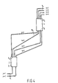
- the phased array has an S shape.
- Figure 4 shows a particular embodiment of this device in the form of a demultiplexer with two input channels U j , four array channels W q and four output channels V k .
- the S shape of the array does not impose the requirement that the length of the channels must increase with increasing q number. Hence, there is more freedom in choosing the parameter r q , which freedom can be used to modify the wavelength transmission characteristics of the device.
- the length increment of each array channel i.e.
- the lengths of the channels increase monotonically when taking first the odd numbered channels in decreasing order and then the even numbered channels in increasing order.
- Equations (38), (39) and (40) define an arrangement of the channels by specifying the length of a channel as a function of its ordinal number. Other equivalent arrangements may be found by choosing an integer number, adding this to the values of s q as given by eqs. (39) and (40), and taking the new values of s q modulo N.
- the arrangement of the channels shown in Figure 4 is according to eqs. (39) and (40) with the different lengths of the channels implemented by different slopes of a straight intermediate section of each of the channels. The choice in length differences may be increased by using more bends and curved sections in the array channels.
- the channels may also consist of only curved sections, thereby making larger radii of curvature of the bends possible, which in turn reduces the radiation losses in the bends.
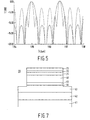
- Figure 5 shows the transmission characteristics of the demultiplexers of Figures 1 and 4.
- the horizontal axis gives the wavelength of the radiation entering input U 1
- the vertical axis gives the transmission T as measured in the reference output channel V 3 .
- the solid line gives the transmission of the demultiplexer with the S-shaped array
- the dashed line the transmission of the demultiplexer with the U-shaped array.
- the reference wavelength ⁇ 0 is 1.550 ⁇ m for which the output channel V 3 shows a maximum and the output channels V 1 , V 2 and V 4 should have a minimum transmission.
- the output channels V 1 , V 2 and V 4 should show a maximum transmission for wavelengths 1.546 ⁇ m, 1.542 ⁇ m and 1.538 ⁇ m, whereas for these wavelengths the output channel V3 has a minimum transmission as shown in Figure 5.
- the latter is a consequence of the design of the device.
- the crosstalk from one output channel to another output channel is zero.
- the transmission minima will not be zero, resulting in a finite crosstalk.
- the influence of the manufacturing tolerances is determined by the width of the transmission minimum around said wavelengths of 1.546, 1.542 and 1.538 ⁇ m. The greater the width, the smaller the influence of the tolerances.
- the width of the minimum for the drawn curve around the wavelength 1.546 nm is twice as wide as that for the dashed curve.
- the device with the S-shaped array will be less affected by manufacturing inaccuracies and, consequently, will have a lower crosstalk than the device with the U-shaped array.
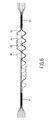
- Figure 6 shows an embodiment of the optical device according to the invention which allows a great variation in pathlengths of the optical channels.
- Two 8x8 MMI's 61, 62 are connected by eight channels.
- Each one of the other channels may comprise one or more bends of substantially identical shape, the pathlength of a channel increasing with the number of bends in the channel.
- a bend may have the shape of a nearly closed ring, half a period of a sinusoid, or a bell, as shown in Figure 6.
- a bend may comprise straight sections and/or circular sections, possibly with different radii of curvature.
- the pathlength need not increase with increasing ordinal number of the channel, as shown by Figure 6.
- the channels 64, 65 and 66 for example, have 6, 2 and 4 bends respectively. Hence, the ordinal numbers of the channels for increasing pathlength is 65, 66, 64.
- the embodiments of the optical device according to the invention described in the preceding paragraphs comprise passive arrays, that is, arrays which are not controllable. However, the arrays can be made active by overlaying channels of the array with electrodes. In this way an electric field or an injection current can be imposed on the channels.
- a cross-section of a channel with an electrode is shown in Figure 7.
- the rib-waveguide structure 70 comprises the same layers 41 to 46 as the rib-waveguide structure 40 shown in Figure 3.
- Layer 46 is covered by a heavily doped p + -InP layer 71 and a heavily doped p + -InGaAs layer 72.
- a metal layer 73, made of for instance a TiPtAu alloy, on top of layer 72 forms a first electrode.
- the substrate 41 forms a second electrode.
- the device is controlled by applying an adjustable voltage across or current through the two electrodes.
- each channel of the array may be overlaid with a separate electrode.
- a desired tuning of the transmission function of the device can be achieved.
- a proper choice of the voltages may compensate the phase differences between optical paths in the MMIs, thereby making the small length increments ⁇ l q of the channels unnecessary.
- the large increments ⁇ L q determine the shape of the transmission function of the device.
- the length of the electrodes is adapted to the ordinal number of the channel it overlays in such a way that the same voltage can be applied to all electrodes.
- the length of an electrode on a channel must then be proportional to the length difference between that channel and a reference channel.
- Figure 8 shows an embodiment of the WDM of Figure 1, provided with electrodes. Channel 1 is chosen as reference channel, and has therefore no electrode.
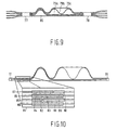
- Figure 9 shows a WDM with a sinusoidal array of the type shown in Figure 6, but with electrodes overlaying the channels.
- the two MMI couplers are indicated by elements 77 and 78.
- a single rectangular electrode may overlay part of each sinusoidal bend in the channels.
- the width of this electrode must be chosen such that the total length of the overlaid parts of a channel is proportional to the length difference between that channel and straight channel 80.
- the electrode may be replaced by one or more small electrodes on each waveguide, which are electrically connected in order to apply an equal voltage on them.
- Channels 79a, b and c in Figure 9 are overlaid with such small electrodes, indicated by heavy lines.
- the length of an electrode on one of the channels is proportional to the length difference between that channel and channel 80.
- Figure 10 shows an embodiment of the WDM of Figure 9 with a different layout of the electrodes.
- the enlargement 81 of the section of the array comprising the electrodes shows three electrodes 82, 83 and 84 arranged on channels 85, 86 and 87 respectively, the electrodes having a length proportional to the length difference between the corresponding channel and the straight channel 80.
- Three dummy electrodes 88, 89 and 90 on channels 80, 85 and 87 respectively have such a length that the total length of each channel overlaid with electrode is equal for all channels. This has the advantage that losses in a channel due to the electrodes are equal for all channels, thereby avoiding a degradation of the crosstalk of the device.
- wavelength demultiplexer Although the invention has been described with reference to a wavelength demultiplexer, it.will be clear that the scope also encompasses wavelength multiplexers, which perform the opposite operation to that of a demultiplexer, and wavelength routers.
- the inherent periodicity of the transmission of the device according to the invention make it very suitable for use in optical communication systems. For instance, a phased array device with a single input channel and a single output channel operates as an optical comb filter. When the length increments ⁇ L q of the array channels in the S-shaped configuration is made equal to zero, the device has no dispersive power and acts as a planar lens.
Landscapes
- Physics & Mathematics (AREA)
- General Physics & Mathematics (AREA)
- Optics & Photonics (AREA)
- Engineering & Computer Science (AREA)
- Microelectronics & Electronic Packaging (AREA)
- Optical Integrated Circuits (AREA)
- Optical Communication System (AREA)
Description



Claims (10)
- An optical device comprising a first coupler (2), a second coupler (3) and a plurality of at least three optical channels (wq) connecting outputs of the first coupler (2) to inputs of the second coupler (3) and forming a dispersive array, characterized in that at least one of the couplers is a multimode-imaging component, phase differences between optical paths in the multimode-imaging component being compensated by differences in optical pathlength of the channels.
- An optical device according to Claim 1, characterized in that differences in optical pathlength between neighbouring channels are substantially equal to an integer function times a basic length, where the value of the function depends on the ordinal numbers of the neighbouring channels in the array.
- An optical device according to Claim 1, characterized in that the first coupler (2) has N outputs and the second coupler (3) has N inputs and N outputs, with N an integer larger than 2.
- An optical device according to Claim 1, characterized in that the at least three optical channels (wq) are configured in an S-shape.
- An optical device according to Claim 4, characterized in that the absolute value of the difference in optical pathlength between an optical channel and a neighbouring optical channel of higher ordinal number is a monotonically increasing function of the ordinal number, and two consecutive differences have different signs.
- An optical device according to Claim 1, characterized in that different optical channels of the array comprise a different number of substantially identical bends.
- An optical device according to Claim 1, characterized in that an electrode overlays at least one channel for introducing phase changes in the at least one channel.
- An optical device according to Claim 7, characterized in that at least two channels are overlaid by one electrode (74, 75, 76) 82, 83, 84).
- An optical device according to Claim 7 or 8, characterized in that the length of a channel overlaid by an electrode (74, 75, 76) is proportional to the difference in optical pathlength between that channel and a reference channel.
- An optical device according to Claim 7, characterized in that each channel is overlaid by at least one of said electrode (82, 83, 84) and a dummy electrode (88, 89, 90), and the total lengths of the channels overlaid by the electrodes are equal.
Priority Applications (1)
| Application Number | Priority Date | Filing Date | Title |
|---|---|---|---|
| EP95906465A EP0695428B1 (en) | 1994-02-11 | 1995-02-09 | Optical device with phased array |
Applications Claiming Priority (8)
| Application Number | Priority Date | Filing Date | Title |
|---|---|---|---|
| EP94200368 | 1994-02-11 | ||
| EP94200368 | 1994-02-11 | ||
| EP94200548 | 1994-03-04 | ||
| EP94200548 | 1994-03-04 | ||
| EP95200182 | 1995-01-26 | ||
| EP95200182 | 1995-01-26 | ||
| EP95906465A EP0695428B1 (en) | 1994-02-11 | 1995-02-09 | Optical device with phased array |
| PCT/IB1995/000084 WO1995022070A1 (en) | 1994-02-11 | 1995-02-09 | Optical device with phased array |
Publications (2)
| Publication Number | Publication Date |
|---|---|
| EP0695428A1 EP0695428A1 (en) | 1996-02-07 |
| EP0695428B1 true EP0695428B1 (en) | 2001-10-10 |
Family
ID=27235965
Family Applications (1)
| Application Number | Title | Priority Date | Filing Date |
|---|---|---|---|
| EP95906465A Expired - Lifetime EP0695428B1 (en) | 1994-02-11 | 1995-02-09 | Optical device with phased array |
Country Status (5)
| Country | Link |
|---|---|
| US (1) | US5862279A (en) |
| EP (1) | EP0695428B1 (en) |
| JP (1) | JP3425150B2 (en) |
| DE (1) | DE69523104T2 (en) |
| WO (1) | WO1995022070A1 (en) |
Families Citing this family (53)
| Publication number | Priority date | Publication date | Assignee | Title |
|---|---|---|---|---|
| DE19506814C2 (en) * | 1995-02-27 | 2001-03-01 | Hertz Inst Heinrich | Spectral apparatus |
| JPH10509536A (en) * | 1995-09-20 | 1998-09-14 | フィリップス、エレクトロニクス、ネムローゼ、フェンノートシャップ | Optical integrated circuit including polarization converter |
| US5661825A (en) * | 1995-09-22 | 1997-08-26 | U.S. Philips Corporation | Integrated optical circuit comprising a polarization convertor |
| FR2753803B1 (en) * | 1996-09-24 | 1998-12-11 | MULTIPLEXER COMPONENT WITH SPECTROGRAPH WITH WAVEGUID ARRAY | |
| EP0950297B1 (en) * | 1996-12-23 | 2002-08-28 | Tellabs Denmark A/S | A bidirectional router and a method of monodirectional amplification |
| JP3487730B2 (en) | 1997-05-30 | 2004-01-19 | 日本電信電話株式会社 | Array waveguide grating element |
| SE521765C2 (en) * | 1997-08-29 | 2003-12-02 | Ericsson Telefon Ab L M | Device and method related to optical transmission |
| JP3045115B2 (en) * | 1997-09-30 | 2000-05-29 | 日本電気株式会社 | Method for manufacturing optical semiconductor device |
| DE19744354C2 (en) * | 1997-10-08 | 2001-02-01 | Hertz Inst Heinrich | Devices for separating and superimposing light signals having different frequency components |
| US6137927A (en) * | 1998-01-16 | 2000-10-24 | Corning Incorporated | N-port reconfigurable DWDM multiplexer and demultiplexer |
| GB2334594A (en) | 1998-02-20 | 1999-08-25 | Fujitsu Telecommunications Eur | Arrayed waveguide grating device |
| AUPP208398A0 (en) * | 1998-03-02 | 1998-03-26 | University Of Melbourne, The | An optical device for dispersion compensation |
| JP3098235B2 (en) * | 1998-08-04 | 2000-10-16 | 日本電信電話株式会社 | Wavelength demultiplexer, optical spectrum analyzer and optical bandpass filter |
| GB9826878D0 (en) * | 1998-12-07 | 1999-01-27 | Northern Telecom Ltd | Duplex optical transmission system |
| US6445477B1 (en) * | 1999-02-11 | 2002-09-03 | Lucent Technologies | Self-monitored light source for stable wavelength optical communications |
| US6181849B1 (en) | 1999-04-30 | 2001-01-30 | Lucent Technologies, Inc. | Interleaved wavelengths multi/demultiplexer with multiple-input-ports and multiple-output-ports for wavelength add/drop WDM systems |
| US6587615B1 (en) | 1999-05-11 | 2003-07-01 | Jds Fitel Inc. | Wavelength multiplexer-demultiplexer having a wide flat response within the spectral passband |
| US6421478B1 (en) * | 1999-05-11 | 2002-07-16 | Jds Fitel Inc. | Tapered MMI coupler |
| KR100296384B1 (en) * | 1999-06-21 | 2001-07-12 | 윤종용 | AWG WDM comprising alignment waveguide and apparatus for aligning it |
| US6415080B1 (en) | 1999-09-03 | 2002-07-02 | Zolo Technologies, Inc. | Echelle grating dense wavelength division multiplexer/demultiplexer |
| JP2001083344A (en) * | 1999-09-10 | 2001-03-30 | Nec Corp | Array waveguide diffraction grating type optical element |
| US6947220B1 (en) | 1999-11-22 | 2005-09-20 | Ksm Associates, Inc. | Devices for information processing in optical communications |
| US6529649B1 (en) * | 2000-05-01 | 2003-03-04 | Lucent Technologies Inc. | Optical filter with improved crosstalk rejection |
| US6298186B1 (en) * | 2000-07-07 | 2001-10-02 | Metrophotonics Inc. | Planar waveguide grating device and method having a passband with a flat-top and sharp-transitions |
| WO2002073267A1 (en) * | 2001-03-13 | 2002-09-19 | Schott Glas | Method for the production of awg couplers and awg coupler |
| GB2373386A (en) * | 2001-03-16 | 2002-09-18 | Fujitsu Network Comm Inc | Compensation for higher order chromatic dispersion |
| US6788837B2 (en) * | 2001-03-27 | 2004-09-07 | Intel Corporation | Method and apparatus for interleaving and switching an optical beam in a semiconductor substrate |
| US6853773B2 (en) * | 2001-04-30 | 2005-02-08 | Kotusa, Inc. | Tunable filter |
| US6597836B2 (en) | 2001-06-20 | 2003-07-22 | The Boeing Company | Optical phased array control system |
| JP3643058B2 (en) * | 2001-07-30 | 2005-04-27 | Tdk株式会社 | Waveguide grating |
| US6766074B1 (en) | 2001-08-15 | 2004-07-20 | Corning Incorporated | Demultiplexer/multiplexer with a controlled variable path length device |
| IL145320A (en) * | 2001-09-06 | 2006-12-10 | Gilad Optical Switches Ltd | Tunable optical filter |
| AU2002353969A1 (en) * | 2001-11-01 | 2003-05-12 | Massachusetts Institute Of Technology | Arrayed waveguide grating |
| JP3737780B2 (en) * | 2002-06-07 | 2006-01-25 | 富士通株式会社 | Wavelength multiplexer / demultiplexer |
| US7242866B2 (en) * | 2002-08-29 | 2007-07-10 | Intel Corporation | Methods and apparatus for switching N optical input signals to M optical outputs |
| JP2005221999A (en) * | 2004-02-09 | 2005-08-18 | Fuji Xerox Co Ltd | Optical modulator and optical modulator array |
| WO2006061783A1 (en) * | 2004-12-10 | 2006-06-15 | Koninklijke Philips Electronics N. V. | Multi-spot investigation apparatus |
| US7433560B2 (en) * | 2005-10-18 | 2008-10-07 | Lucent Technologies Inc. | Rectangular-passband multiplexer |
| US7840104B2 (en) * | 2007-07-13 | 2010-11-23 | Enablence USA Components, Inc. | Ultra-wide band AWG multiplexer |
| US9344196B1 (en) | 2009-05-28 | 2016-05-17 | Freedom Photonics, Llc. | Integrated interferometric optical transmitter |
| US8401399B2 (en) | 2009-05-28 | 2013-03-19 | Freedom Photonics, Llc. | Chip-based advanced modulation format transmitter |
| JP5713378B2 (en) * | 2009-11-20 | 2015-05-07 | 国立大学法人九州大学 | Waveguide type optical filter and semiconductor laser |
| JP2012013886A (en) * | 2010-06-30 | 2012-01-19 | Fujitsu Ltd | Optical waveguide element, optical hybrid circuit, and optical receiver |
| JP5817147B2 (en) * | 2011-02-25 | 2015-11-18 | 国立大学法人九州大学 | Optical filter |
| JP5720354B2 (en) * | 2011-03-25 | 2015-05-20 | 富士通株式会社 | Optical waveguide device and optical hybrid circuit |
| US20130119270A1 (en) * | 2011-11-16 | 2013-05-16 | Samsung Electronics Co., Ltd. | Wavelength division devices, multi-wavelength light generators and optical biosensor systems using the same |
| JP2014191088A (en) * | 2013-03-26 | 2014-10-06 | Nippon Telegr & Teleph Corp <Ntt> | Optical wavelength filter |
| GB2530317A (en) | 2014-09-19 | 2016-03-23 | Univ Southampton | Optical (DE)Multiplexers |
| JP6233342B2 (en) * | 2015-03-31 | 2017-11-22 | 住友大阪セメント株式会社 | Light modulator |
| DE102015225863A1 (en) * | 2015-12-18 | 2017-06-22 | Robert Bosch Gmbh | Optical phased array and LiDAR system |
| WO2017151843A1 (en) * | 2016-03-02 | 2017-09-08 | The Government Of The United States Of America, As Represented By The Secretary Of The Navy Naval | Chip-scale two-dimensionai optical phased array with simplified controls |
| US10320152B2 (en) | 2017-03-28 | 2019-06-11 | Freedom Photonics Llc | Tunable laser |
| GB2575653A (en) * | 2018-07-17 | 2020-01-22 | Univ College Cork National Univ Of Ireland | Phase modulator for optical signal using multimode interference couplers |
Family Cites Families (22)
| Publication number | Priority date | Publication date | Assignee | Title |
|---|---|---|---|---|
| US4768850A (en) * | 1984-06-20 | 1988-09-06 | The Board Of Trustees Of The Leland Stanford Junior University | Cascaded fiber optic lattice filter |
| AU569803B2 (en) * | 1984-09-06 | 1988-02-18 | Hitachi Limited | Optical fibre star coupler |
| US4900119A (en) * | 1988-04-01 | 1990-02-13 | Canadian Patents & Development Ltd. | Wavelength selective optical devices using optical directional coupler |
| US5002350A (en) * | 1990-02-26 | 1991-03-26 | At&T Bell Laboratories | Optical multiplexer/demultiplexer |
| FR2664992A1 (en) * | 1990-07-19 | 1992-01-24 | Centre Nat Rech Scient | ELECTRO-OPTICAL MICROWAVE MODULATOR WITH CONTINUOUS POLARIZATION OF THE GUIDE. |
| GB9027656D0 (en) * | 1990-12-20 | 1991-02-13 | Secr Defence | Signal routing device |
| GB9027657D0 (en) | 1990-12-20 | 1991-02-13 | Secr Defence | Optical device |
| US5247594A (en) * | 1991-03-22 | 1993-09-21 | Nippon Telegraph And Telephone Corporation | Waveguide-type optical matrix switch |
| US5119453A (en) * | 1991-04-05 | 1992-06-02 | Ecole Polytechnique | Wavelength-flattened 2x2 splitter for single-mode optical waveguides and method of making same |
| NL9101532A (en) * | 1991-09-10 | 1993-04-01 | Nederland Ptt | WAVE LENGTH-SELECTIVE MULTIPLEXER AND DEMULTIPLEXER. |
| US5212758A (en) * | 1992-04-10 | 1993-05-18 | At&T Bell Laboratories | Planar lens and low order array multiplexer |
| GB9212727D0 (en) * | 1992-06-16 | 1992-07-29 | Secr Defence | Radiation coupling device |
| US5243672A (en) * | 1992-08-04 | 1993-09-07 | At&T Bell Laboratories | Planar waveguide having optimized bend |
| US5351317A (en) * | 1992-08-14 | 1994-09-27 | Telefonaktiebolaget L M Ericsson | Interferometric tunable optical filter |
| DE69311048T2 (en) * | 1992-09-29 | 1997-12-11 | Nippon Telegraph & Telephone | Multi / demultiplexer with grating of grouped waveguides and returned optical paths |
| US5367586A (en) * | 1993-03-26 | 1994-11-22 | At&T Bell Laboratories | Optical delay line |
| US5461685A (en) * | 1993-10-18 | 1995-10-24 | At&T Ipm Corp. | Optical passband filter |
| US5425116A (en) * | 1993-11-16 | 1995-06-13 | At&T Corp. | Tunable optical waveguide grating arrangement |
| DE59502068D1 (en) * | 1994-01-11 | 1998-06-10 | Siemens Ag | Optical arrangement of strip-shaped optical waveguides |
| US5412744A (en) * | 1994-05-02 | 1995-05-02 | At&T Corp. | Frequency routing device having a wide and substantially flat passband |
| US5467418A (en) * | 1994-09-02 | 1995-11-14 | At&T Ipm Corp. | Frequency routing device having a spatially filtered optical grating for providing an increased passband width |
| US5636300A (en) * | 1994-12-12 | 1997-06-03 | Corning Incorporated | MxO multiplex demultiplex component |
-
1995
- 1995-02-09 EP EP95906465A patent/EP0695428B1/en not_active Expired - Lifetime
- 1995-02-09 DE DE69523104T patent/DE69523104T2/en not_active Expired - Fee Related
- 1995-02-09 JP JP52109695A patent/JP3425150B2/en not_active Expired - Fee Related
- 1995-02-09 WO PCT/IB1995/000084 patent/WO1995022070A1/en not_active Ceased
-
1997
- 1997-04-10 US US08/838,817 patent/US5862279A/en not_active Expired - Fee Related
Non-Patent Citations (1)
| Title |
|---|
| BESSE, P.A. ET AL: "PHASE RELATIONS IN MULTIMODE INTERFERENCE COUPLERS AND THEIR APPLICATION TO GENERALIZED INTEGRATED MACH-ZEHNDER OPTICAL SWITCHES", PROCEEDINGS OF THE EUROPEN CONFERENCE ON INTEGRATED OPTICS, APRIL 18-22,1993, pages 2 - 22-2-23 * |
Also Published As
| Publication number | Publication date |
|---|---|
| WO1995022070A1 (en) | 1995-08-17 |
| JPH08509079A (en) | 1996-09-24 |
| EP0695428A1 (en) | 1996-02-07 |
| US5862279A (en) | 1999-01-19 |
| DE69523104T2 (en) | 2002-06-06 |
| DE69523104D1 (en) | 2001-11-15 |
| JP3425150B2 (en) | 2003-07-07 |
Similar Documents
| Publication | Publication Date | Title |
|---|---|---|
| US5862279A (en) | Optical device with phased array | |
| Smit et al. | PHASAR-based WDM-devices: Principles, design and applications | |
| EP0528652B1 (en) | Improved optical multiplexer, and demultiplexer | |
| US7356224B2 (en) | Method and apparatus for detecting multiple optical wave lengths | |
| EP0903616B1 (en) | Switchable optical filter | |
| US20090180736A1 (en) | Method and apparatus for detecting multiple optical wavelengths | |
| JP2693354B2 (en) | Optical device | |
| EP0822428A1 (en) | Method and apparatus for atomic absorption-spectroscopy | |
| WO2002088806A1 (en) | Planar holographic multiplexer/demultiplexer | |
| US6442308B1 (en) | Optical wavelength multiplexer/demultiplexer with uniform loss | |
| Augustsson | Bragg grating-assisted MMI-coupler for add-drop multiplexing | |
| US20230288636A1 (en) | Super-compact arrayed waveguide grating (awg) wavelength division multiplexer based on sub-wavelength grating | |
| US20030206681A1 (en) | Integrating element for optical fiber communication systems based on photonic multi-bandgap quasi-crystals having optimized transfer functions | |
| CA2490768A1 (en) | Method and apparatus for detecting multiple optical wave lengths | |
| US5978532A (en) | Spectrographic multiplexer component having an array of waveguides | |
| US6787868B1 (en) | Microlenses for integrated optical devices | |
| EP1430342B1 (en) | Passband flattening in an arrayed waveguide grating | |
| AU765250B2 (en) | Optical components | |
| Amersfoort et al. | Optical device with phased array | |
| Osgood jr et al. | Imaging Devices | |
| US6650796B2 (en) | Waveguide optical frequency router | |
| Augustsson | Proposal of a wavelength-selective switch based on an MMIMZI configuration with wavelength-selective phase-tuning circuits | |
| US7058262B2 (en) | Arrayed waveguide grating | |
| US6522811B1 (en) | Arrayed waveguide grating | |
| EP1257859A1 (en) | Grating waveguide configuration for phasars |
Legal Events
| Date | Code | Title | Description |
|---|---|---|---|
| PUAI | Public reference made under article 153(3) epc to a published international application that has entered the european phase |
Free format text: ORIGINAL CODE: 0009012 |
|
| AK | Designated contracting states |
Kind code of ref document: A1 Designated state(s): DE FR GB IT NL SE |
|
| 17P | Request for examination filed |
Effective date: 19960219 |
|
| 17Q | First examination report despatched |
Effective date: 19980824 |
|
| GRAG | Despatch of communication of intention to grant |
Free format text: ORIGINAL CODE: EPIDOS AGRA |
|
| GRAG | Despatch of communication of intention to grant |
Free format text: ORIGINAL CODE: EPIDOS AGRA |
|
| GRAH | Despatch of communication of intention to grant a patent |
Free format text: ORIGINAL CODE: EPIDOS IGRA |
|
| GRAH | Despatch of communication of intention to grant a patent |
Free format text: ORIGINAL CODE: EPIDOS IGRA |
|
| GRAA | (expected) grant |
Free format text: ORIGINAL CODE: 0009210 |
|
| AK | Designated contracting states |
Kind code of ref document: B1 Designated state(s): DE FR GB IT NL SE |
|
| PG25 | Lapsed in a contracting state [announced via postgrant information from national office to epo] |
Ref country code: NL Free format text: LAPSE BECAUSE OF FAILURE TO SUBMIT A TRANSLATION OF THE DESCRIPTION OR TO PAY THE FEE WITHIN THE PRESCRIBED TIME-LIMIT Effective date: 20011010 Ref country code: IT Free format text: LAPSE BECAUSE OF FAILURE TO SUBMIT A TRANSLATION OF THE DESCRIPTION OR TO PAY THE FEE WITHIN THE PRE;WARNING: LAPSES OF ITALIAN PATENTS WITH EFFECTIVE DATE BEFORE 2007 MAY HAVE OCCURRED AT ANY TIME BEFORE 2007. THE CORRECT EFFECTIVE DATE MAY BE DIFFERENT FROM THE ONE RECORDED.SCRIBED TIME-LIMIT Effective date: 20011010 |
|
| REF | Corresponds to: |
Ref document number: 69523104 Country of ref document: DE Date of ref document: 20011115 |
|
| REG | Reference to a national code |
Ref country code: GB Ref legal event code: IF02 |
|
| PG25 | Lapsed in a contracting state [announced via postgrant information from national office to epo] |
Ref country code: SE Free format text: LAPSE BECAUSE OF FAILURE TO SUBMIT A TRANSLATION OF THE DESCRIPTION OR TO PAY THE FEE WITHIN THE PRESCRIBED TIME-LIMIT Effective date: 20020110 |
|
| ET | Fr: translation filed | ||
| NLV1 | Nl: lapsed or annulled due to failure to fulfill the requirements of art. 29p and 29m of the patents act | ||
| PLBE | No opposition filed within time limit |
Free format text: ORIGINAL CODE: 0009261 |
|
| STAA | Information on the status of an ep patent application or granted ep patent |
Free format text: STATUS: NO OPPOSITION FILED WITHIN TIME LIMIT |
|
| 26N | No opposition filed | ||
| REG | Reference to a national code |
Ref country code: GB Ref legal event code: 746 Effective date: 20021014 |
|
| REG | Reference to a national code |
Ref country code: FR Ref legal event code: D6 |
|
| PGFP | Annual fee paid to national office [announced via postgrant information from national office to epo] |
Ref country code: FR Payment date: 20040226 Year of fee payment: 10 |
|
| PGFP | Annual fee paid to national office [announced via postgrant information from national office to epo] |
Ref country code: GB Payment date: 20040227 Year of fee payment: 10 |
|
| PGFP | Annual fee paid to national office [announced via postgrant information from national office to epo] |
Ref country code: DE Payment date: 20040415 Year of fee payment: 10 |
|
| PG25 | Lapsed in a contracting state [announced via postgrant information from national office to epo] |
Ref country code: GB Free format text: LAPSE BECAUSE OF NON-PAYMENT OF DUE FEES Effective date: 20050209 |
|
| PG25 | Lapsed in a contracting state [announced via postgrant information from national office to epo] |
Ref country code: DE Free format text: LAPSE BECAUSE OF NON-PAYMENT OF DUE FEES Effective date: 20050901 |
|
| GBPC | Gb: european patent ceased through non-payment of renewal fee |
Effective date: 20050206 |
|
| PG25 | Lapsed in a contracting state [announced via postgrant information from national office to epo] |
Ref country code: FR Free format text: LAPSE BECAUSE OF NON-PAYMENT OF DUE FEES Effective date: 20051031 |
|
| REG | Reference to a national code |
Ref country code: FR Ref legal event code: ST Effective date: 20051031 |