EP0694199B1 - Grid and method of manufacturing such grid - Google Patents
Grid and method of manufacturing such grid Download PDFInfo
- Publication number
- EP0694199B1 EP0694199B1 EP94915293A EP94915293A EP0694199B1 EP 0694199 B1 EP0694199 B1 EP 0694199B1 EP 94915293 A EP94915293 A EP 94915293A EP 94915293 A EP94915293 A EP 94915293A EP 0694199 B1 EP0694199 B1 EP 0694199B1
- Authority
- EP
- European Patent Office
- Prior art keywords
- spacers
- laminations
- grid
- package
- guides
- Prior art date
- Legal status (The legal status is an assumption and is not a legal conclusion. Google has not performed a legal analysis and makes no representation as to the accuracy of the status listed.)
- Expired - Lifetime
Links
Images


Classifications
-
- G—PHYSICS
- G21—NUCLEAR PHYSICS; NUCLEAR ENGINEERING
- G21K—HANDLING OF PARTICLES OR IONISING RADIATION NOT OTHERWISE PROVIDED FOR; IRRADIATION DEVICES; GAMMA RAY OR X-RAY MICROSCOPES
- G21K1/00—Arrangements for handling particles or ionising radiation, e.g. focusing or moderating
- G21K1/02—Arrangements for handling particles or ionising radiation, e.g. focusing or moderating using diaphragms, collimators
- G21K1/025—Arrangements for handling particles or ionising radiation, e.g. focusing or moderating using diaphragms, collimators using multiple collimators, e.g. Bucky screens; other devices for eliminating undesired or dispersed radiation
Definitions
- the radiation is incident on the first array and is transmitted or absorbed depending on the angle of incidence.
- the transmitted part of the radiation is incident on the second array and there, too, is transmitted or absorbed depending on the angle of incidence.
- Behind the second array a detection surface with radiation detectors is arranged.
- the radiation incident on the detection surface provides, upon detection and subsequent signal processing, an image of the source of radiation.
- the slit width of the grids in an array should vary from about 4 mm to about 50 ⁇ m.
- the distance between the centers of two adjacent slits, to be referred to as pitch is about 100 ⁇ m and the deviation of the slit width should not exceed a few microns.
- the resolution of the detection device is determined by the grid having the smallest slit width and by the relative distance of the arrays.
- the present grids must have a thickness of at least about 3 mm.
- the ratio between the height and the width of a slit is therefore at least 60:1.
- Such a pattern can no longer be manufactured by means of etching technique.
- the object of the present invention is to provide a grid which satisfies the above stated requirements and with which the problems of the prior art are solved.
- the invention provides a slit pattern, to be referred to as grid, which comprises the features of claim 1.
- the grid is characterized, in accordance with a further elaboration of the invention, in that the spacers have a thickness substantially corresponding with the desired pitch of the slits, the spacers being of reduced thickness over a part of their surface, so that, upon stacking of the spacers, between two consecutive spacers an opening is present in which a lamination is slidably receivable.
- a grid with thus designed spacers has the advantage that the pitch of the slits is exclusively determined by the thickness of the spacers, whereas the pitch of the slits of a grid which has been formed by alternately stacking laminations and spacers is additionally determined by the thickness of the laminations.
- the grid designed with spacers which are of reduced thickness over a part of their surface has half the number of pitch determining contact surfaces. Through the reduction of the number of contact surfaces, the possibility of the occurrence of positional deviations of the laminations is reduced by half.
- the grid is characterized, in accordance with a further elaboration of the invention, in that the spacers are so designed that a plurality of spacers stacked to form a package are compressible against spring force.
- the exemplary embodiment shown in the drawing comprises a frame made up of a U-shaped part 1 and a closing beam 2.
- the frame further comprises a plurality of guides 3 over which spacers 4 (Figs. 3, 4, 5) can be fitted.
- the spacers 4 keep laminations 5 spaced.
- the representation of the grid shown in Fig. 1 is approximately full-size, with the proviso that the distance between the laminations 5 is depicted to an enlarged scale for drawing-technical reasons.
- the real distance between the laminations is 50 ⁇ m.
- a package of spacers 17 having a high spring constant Located between two pairwise facing reference faces 15 is a package of spacers 17 having a high spring constant.
- the outermost spacers 4a of the rigid package of spacers 17 each abut against a support plate 16 and 16a, respectively, which, in turn, each abut against the facing reference faces 15.
- the package of spacers 17 having the high spring constant presses the support plates 16, 16a with force against the reference faces 15. Since the thickness of the support plates 16, 16a is accurately defined, the outermost spacers of the rigid package 17 are located in the desired positions. Positional deviations of laminations 5 due to accumulation of thickness deviations of the spacers 4 can now only occur within the package 17.
- the spacers 4a, 4b, 4c, 4d are manufactured by means of photochemical etching. The manufacture takes place in two exposure and two etching steps, a stainless steel sheet of a thickness of 100 ⁇ m being used as starting material. The stainless steel sheet is treated with photoresist.
- the lacquer around the outer contours of the spacers, except for some points of attachment is exposed.
- the first etching step the material which has been exposed, apart from the unexposed points of attachment, is removed completely by etching.
- the spacers 4 are connected with the stainless steel sheet only through the points of attachment.
- parts 8, 9 of the surface of the spacers 4 are exposed.
- the spacers 4 and laminations 5 can be assembled by stacking them alternately. Positioning of the spacers 4 and the laminations 5 is effected by fitting the support plates 16. Finally, a closing beam 2 is placed on the U-shaped frame 1, whereafter the grid is ready for assembly in an array.
Landscapes
- Physics & Mathematics (AREA)
- Spectroscopy & Molecular Physics (AREA)
- Engineering & Computer Science (AREA)
- General Engineering & Computer Science (AREA)
- High Energy & Nuclear Physics (AREA)
- Measurement Of Radiation (AREA)
- Packaging Of Annular Or Rod-Shaped Articles, Wearing Apparel, Cassettes, Or The Like (AREA)
Abstract
Description
- This invention relates to a slit pattern, to be referred to as grid, and a method for the manufacture thereof.
- In particular the invention relates to a slit pattern according to the preamble of
claim 1. - Such a slit pattern or grid is e.g. disclosed in FR-A-2 657 192 or in Nuclear Instruments and Methods 108 (1973), pages 107-111.
- The present grids which are the object of this invention are intended in particular for observing electromagnetic radiation, in particular X-radiation and gamma-radiation, using satellites. A detection device for observing such radiation generally comprises two so-called arrays, each comprising a plurality of grids, and a detection surface made up of radiation detectors. Each grid has a surface area in the range of from 50 mm by 50 mm to 200 mm by 200 mm. An array comprises, for instance, 32 grids, each grid having a different slit width and/or slit direction. The two arrays are identical and are arranged in spaced parallel relationship perpendicularly above each other. A suitable distance between the two arrays is, for instance, 6 m. The radiation is incident on the first array and is transmitted or absorbed depending on the angle of incidence. The transmitted part of the radiation is incident on the second array and there, too, is transmitted or absorbed depending on the angle of incidence. Behind the second array a detection surface with radiation detectors is arranged. The radiation incident on the detection surface provides, upon detection and subsequent signal processing, an image of the source of radiation.
- The slit width of the grids in an array should vary from about 4 mm to about 50 µm. For a grid of a slit width of about 50 µm, the distance between the centers of two adjacent slits, to be referred to as pitch, is about 100 µm and the deviation of the slit width should not exceed a few microns. The resolution of the detection device is determined by the grid having the smallest slit width and by the relative distance of the arrays.
- In itself it is no problem to manufacture a slit pattern of a slit width of 50 µm and a pitch of 100 µm in thin material. This is simple to realize by means of etching techniques.
- However, the problem is that the present grids must have a thickness of at least about 3 mm. The ratio between the height and the width of a slit is therefore at least 60:1. Such a pattern can no longer be manufactured by means of etching technique.
- Moreover, the grids must be resistant to the vibrations than occur upon the launching of the satellite in which the grids are disposed and to the large temperature fluctuations that occur when the satellite moves from the sunlight into the shade or vice versa.
- A further problem which occurs with the manufacture of grids is that when the thickness of the spacers deviates from the nominal thickness, the desired pitch between the slits is not achieved. However, the spacers can be manufactured in such a manner that the deviation in the thickness of the spacers is very slight. On the other hand, by stacking the spacers, each very slight deviation is successively added to the preceding deviation. Thus, stacking a large number of spacers which themselves are manufactured with an accurate thickness still leads to an unacceptable positional deviation through cumulation of the deviations in the thickness of the spacers.
- The object of the present invention is to provide a grid which satisfies the above stated requirements and with which the problems of the prior art are solved.
- To that end, the invention provides a slit pattern, to be referred to as grid, which comprises the features of
claim 1. - A grid thus built up offers the advantage that the separate parts thereof, such as the laminations and the spacers, can be manufactured in a highly accurate manner at relatively slight cost and that after assembly, which in essence does not amount to more than stacking the separate spacers onto each other with interposition of the separate laminations, a grid is obtained which satisfies the stated requirements. The presence of the guides provides the advantage that the laminations are distanced by spacers at several points along their length, so that the chances of the laminations bending relative to each other, which would disturb the slit pattern, are reduced to a minimum.
- Because of the guides with the reference faces the laminations are not only distanced by spacers at several points along their length but also accurately positioned by the reference faces provided on the guides, so that any bending of the laminations, not only with respect to each other but also with respect to the nominally desired positions, is prevented. Moreover, a grid with guides of such design offers the advantage that the positional error resulting from cumulation of thickness deviations of the spacers per package of spacers included between two reference faces is reduced to zero. A positional error can only occur within a package due to deviations in the thickness of the spacers within the package. However, because of the limited number of spacers within a package, the positional error remains within the specified margins. Still another advantage of the use of guides provided with reference faces is that the thermal expansion or shrinkage of the grid in the direction perpendicular to the main surfaces of the laminations is exclusively determined by the coefficient of thermal expansion of the guides. Such expansion can be kept small by a suitable choice of the material of the guides.
- In order to allow the laminations to freely expand and shrink in longitudinal direction, which is of importance with a view to maintaining the accuracy of the grid when it is exposed to temperature fluctuations, the grid is characterized, in accordance with a further elaboration of the invention, in that the spacers have a thickness substantially corresponding with the desired pitch of the slits, the spacers being of reduced thickness over a part of their surface, so that, upon stacking of the spacers, between two consecutive spacers an opening is present in which a lamination is slidably receivable.
- Moreover, a grid with thus designed spacers has the advantage that the pitch of the slits is exclusively determined by the thickness of the spacers, whereas the pitch of the slits of a grid which has been formed by alternately stacking laminations and spacers is additionally determined by the thickness of the laminations. Compared with a grid which has been formed by alternately stacking laminations and spacers, the grid designed with spacers which are of reduced thickness over a part of their surface has half the number of pitch determining contact surfaces. Through the reduction of the number of contact surfaces, the possibility of the occurrence of positional deviations of the laminations is reduced by half.
- In order to provide a stable stacking of the spacers, it is particularly advantageous if, in accordance with a further elaboration of the invention, the guides and the spacers are so designed that each spacer is secured by a guide against displacements at least in directions parallel to the main surfaces of the laminations.
- A thus designed grid provides for stable stacking of spacers. (A part of this paragraph and the following three original paragraphs have been deleted)
- A problem encountered when a package made up of a limited number of spacers is included between two reference faces is that as a result of the inaccuracy in the thickness of the spacers in the package, the space between two reference faces is just too large or just too small for the number of spacers to be accommodated. If the space is too large, this gives rise to play between the spacers, which adversely affects the accuracy of the grid. If the space between the reference faces is too small, one spacer must be omitted from the package of spacers, which in turn leads to too large a space between the reference faces for the associated package of spacers, with the above-mentioned disadvantages.
- In order to remove these problems, the grid is characterized, in accordance with a further elaboration of the invention, in that the spacers are so designed that a plurality of spacers stacked to form a package are compressible against spring force.
- A package which is formed by spacers of such design can be clamped between two reference faces without play. Moreover, the position of the laminations of the compressible package, for each lamination present in the package, is related to the reference face and through the compression a positional error built up through cumulation of the deviations in thickness of spacers is evenly distributed over the laminations disposed in the package.
- It is particularly advantageous if, in accordance with a further elaboration of the invention, the reference faces of the guides face each other in pairs and that a package of spacers which has a high spring constant is located between facing reference faces, the spacers of such rigid package that are located on the outsides being in abutment, with or without interposition of a support plate, against the facing reference faces, while a package of spacers having a lower spring constant is clamped between two rigid packages.
- A grid of such design offers the advantage that the outermost spacers of the rigid package are pressed against the reference faces or against the support plate located on the reference face with a relatively great force, so that these spacers are located in the proper and desired position. The outermost spacers of the weak package, which is clamped between two rigid packages, are likewise located in the desired position because they are in abutment, with or without interposition of an intermediate element, against the outermost spacers of the rigid package. The weak package is more inclined to compress than the rigid packages bounding the weak package, so that the outermost spacers of rigid packages retain the position related to the reference faces and thereby the outermost spacers of the weak package also acquire a desired position. The intermediate element may for instance be a spacer which has been shortened to leave free space for the support plate located against the reference face.
- The invention further relates to a method for the manufacture of a slit pattern, to be referred to as grid, at least comprising distancing elements, to be referred to as spacers, and laminations.
- In the method according to the invention, the spacers are manufactured by means of a photochemical etching process from sheet material having a thickness corresponding with the desired pitch of the grid, the grid being assembled by alternately stacking the laminations and the spacers.
- Manufacturing the spacers by means of etching provides the possibility of dimensioning the spacers with great accuracy.
- In order to reduce the thickness of a part of the surface of the spacers, the photochemical etching process is carried out in two steps, wherein in a first step the photolayer on the sheet material is exposed in such a manner that after exposure in the first etching step the material around the outer contours of the spacers, except for a few points of attachment, is removed, and wherein in a second step the photolayer on the sheet material is exposed in such a manner that after exposure in the second etching step a part of the surface of the spacers is removed, so that the thickness of the spacers at the location of the parts exposed in the second step is reduced.
- It will be clear that in the removal of only a layer of sheet material for the reduction of the thickness thereof, the concentration of the etching fluid and the duration of the etching operations must be selected with great precision.
- To clarify the invention, one exemplary embodiment of a grid and a method for the manufacture thereof will be described with reference to the drawing.
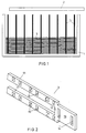
- Fig. 1 is a front elevation of an exemplary embodiment of the grid according to the invention;
- Fig. 2 is a perspective view of a guide;
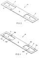
- Fig. 3 is a perspective view of a non-resilient spacer;
- Fig. 4 is a perspective view of a resilient spacer having a relatively high spring constant;
- Fig. 5 is a perspective view of a resilient spacer having a relatively low spring constant;
- Fig. 6 is a perspective view of the way in which spacers are stacked around a reference face of a guide; and
- Fig. 7 is an enlarged view of a part of the sectional elevation taken on line VII-VII in Fig. 1.
- The exemplary embodiment shown in the drawing comprises a frame made up of a
U-shaped part 1 and aclosing beam 2. The frame further comprises a plurality ofguides 3 over which spacers 4 (Figs. 3, 4, 5) can be fitted. The spacers 4 keeplaminations 5 spaced. The representation of the grid shown in Fig. 1 is approximately full-size, with the proviso that the distance between thelaminations 5 is depicted to an enlarged scale for drawing-technical reasons. In the present exemplary embodiment, the real distance between the laminations is 50 µm. - As shown in Figs. 3-5, the
spacers apertures 6 near their short sides. Thespacers central portion 8, between the twoapertures 6, of the surface of thespacers spacers central portion 8. Accordingly, when thespacers central portions 8 of reduced thickness, thelaminations 5 being slidably receivable in theseopenings 7. Thecentral portions 8 of thespacers laminations 5. Thespacer 4a shown in Fig. 3 has its original thickness at thesurfaces 9 bounding theaperture 6, so that a collection ofspacers 4a of this type, stacked to form a package, is not compressible. Thesurfaces 9 bounding theapertures 6 of thespacers 4b, 4c shown in Figs. 4 and 5 have partly been rendered thinner. The thinner portions have been provided in such a manner that thesurfaces 9 bounding the longitudinal edges of theaperture 6 comprise two thickenedwalls 10a on one side of theaperture 6 and one thickenedwall 10b on the other side. In the case of thesurface 9 bounding theaperture 6 and comprising thesingle wall 10b, thewall 10b is provided centrally of the longitudinal edge of theaperture 6. In the case of thesurface 9 bounding theaperture 6 and comprising twowalls 10a, thewalls 10a are arranged near the ends of the longitudinal edge of theaperture 6. A package composed of spacers alternately of the type shown in Fig. 3 and Figs. 4 or 5, with thespacers 4b, 4c of the type shown in Figs. 4 or 5 being stacked in such a manner that opposite awall 10 a reduced surface portion of the next resilient spacer is located, is compressible against spring force. The width of the walls 10 determines the spring constant of a package ofspacers 4b, 4c. According as the walls 10 are wider, the rigidity of the package increases. Fig. 7 clearly shows in what way thespacers - The
guides 3 are substantially U-shaped. Thelegs 11 of theguides 3 have such dimensions and are positioned in such a manner that they correspond with theapertures 6 in thespacers spacers guides 3 and thus be stacked. Thelaminations 5 extend between thelegs 11 of aguide 3, perpendicularly to thisguide 3. Thebase 12 of theguide 3 comprises afoot 13, which fits into a socket (not shown) provided in the base la of theU-shaped frame 1. In the exemplary embodiment shown, thefoot 13 is provided with twoparallel slots 14 in which two parallel leaf springs (not shown) are receivable, which leaf springs are connected adjacent the socket with the base la of theU-shaped frame 1. The leaf springs serve for positioning theguides 3 in the longitudinal direction thereof. After being positioned in theframe 1, theguides 3 can be fixed by means of a securing nut (not shown) or by means of lacquer. The positioning of theguides 3 in their longitudinal direction is of great importance since theguides 3 are provided with a plurality ofapertures 13 evenly spaced apart in thelegs 11, in which apertures 13 onereference face 15 is provided, extending perpendicularly to the longitudinal direction of theguides 3. The reference faces 15 face each other in pairs. In the assembled condition of the grid, asupport plate 16 abuts against eachreference face 15, thesupport plate 16 projecting outside theguide 3 on opposite sides thereof. The parts of thesupport plate 16 projecting outside theguide 3 serve as an abutting surface for a spacer. Located between two pairwise facing reference faces 15 is a package ofspacers 17 having a high spring constant. Theoutermost spacers 4a of the rigid package ofspacers 17 each abut against asupport plate spacers 17 having the high spring constant presses thesupport plates support plates rigid package 17 are located in the desired positions. Positional deviations oflaminations 5 due to accumulation of thickness deviations of the spacers 4 can now only occur within thepackage 17. When thepackage 17 comprises no more than 50, and preferably no more than 35 spacers, the positional deviations within the package remain within the tolerance limits. Preferably, the thickness of thesupport plate 16 corresponds with the thickness of the spacers 4. At the location of thesupport plate 16, ashort spacer 4d (see Figs. 6 and 7) can be included to fill up the gap produced by thesupport plate 16. Between tworigid packaqes 17, a package ofspacers 18 having a lower spring constant is included, theoutermost spacers 4a thereof resting against theshort spacer 4d and the side of thesupport plate 16 proximal to thereference face 15. Because therigid package 17 presses thesupport plate 16 against thereference face 15 with more force than the force with which theweak package 18 presses thesupport plate 16 off thereference face 15, the positions of theoutermost spacers 4a of both the rigid package ofspacers 17 and the weak package ofspacers 18 are accurately related to thereference face 15. - The
spacers parts parts laminations 5 of the grid may for instance be manufactured from rolled-flat tungsten wire.Such laminations 5 have a good surface quality, a very constant thickness and exhibit no burrs or any other detrimental unevennesses. Theframe 1 and theguides 3 may be manufactured from, for instance, an iron-nickel-cobalt alloy by means of spark erosion. - After the
guides 3 have been placed in theframe 1 and accurately positioned in the longitudinal direction, the spacers 4 andlaminations 5 can be assembled by stacking them alternately. Positioning of the spacers 4 and thelaminations 5 is effected by fitting thesupport plates 16. Finally, aclosing beam 2 is placed on theU-shaped frame 1, whereafter the grid is ready for assembly in an array.
Claims (7)
- A slit pattern, to be referred to as grid, comprising a plurality of laminations (5) arranged parallel, which, to form a slit pattern, are maintained in spaced relation by distancing elements, to be referred to as spacers (4) arranged between the laminations, characterized by a plurality of guides (3) distributed along the length of the laminations (5) and extending perpendicularly to the main surfaces of the laminations, the guides being connected with a frame so as to be positionable and fixable in a direction perpendicular to the main surfaces of the laminations (5) and the guides (3) comprising reference faces (15) distributed along the length of the guides, a package (17,18) of a limited number of spacers being receivable between said reference faces.
- A grid according to claim 1, characterized in that the spacers have a thickness substantially corresponding with the desired pitch of the slits, the spacers being of reduced thickness over a part of their surface, so that, upon stacking of the spacers, between two consecutive spacers an opening is present in which a lamination is slidably receivable.
- A grid according to claim 1 or 2, characterized in that the guides and the spacers are so designed that each spacer is secured by a guide against displacements at least in directions parallel to the main surfaces of the laminations.
- A grid according to claim 3, characterized in that the spacers are so designed that a plurality of spacers stacked to form a package are compressible against spring force.
- A grid according to claim 4, characterized in that the reference faces of the guides face each other in pairs and that a package (17) of spacers which has a high spring constant is located between facing reference faces, the spacers of such rigid package (17) that are located on the outsides being in abutment, with or without interposition of a support plate, against the facing reference faces, while a package (18) of spacers which has a lower spring constant is clamped between two rigid packages.
- A method for the manufacture of a slit pattern, to be referred to as grid, comprising at least distancing elements, to be referred to as spacers, and laminations, wherein the spacers are manufactured by means of a photochemical etching process from sheet material having a thickness corresponding with the desired pitch between slits of the grid formed by the laminations, the grid being assembled by alternately stacking the laminations and the spacers.
- A method according to claim 6, characterized in that, in order to reduce the thickness of a part of the surface of the spacers, the photochemical etching process is carried out in two steps, wherein in a first step the photolayer on the sheet material is exposed in such a manner that in the first etching step the material around the outer contours of the spacers, except for some points of attachments, is removed, and wherein in a second step the photolayer on the sheet material is exposed in such a manner that after exposure in the second etching step a part of the surface of the spacers is removed, so that the thickness of the spacers at the location of the parts exposed in the second step is reduced.
Applications Claiming Priority (3)
| Application Number | Priority Date | Filing Date | Title |
|---|---|---|---|
| NL9300654A NL9300654A (en) | 1993-04-16 | 1993-04-16 | Grid to be called a slit pattern and a method for the manufacture thereof. |
| NL9300654 | 1993-04-16 | ||
| PCT/NL1994/000078 WO1994024676A1 (en) | 1993-04-16 | 1994-04-15 | Grid and method of manufacturing such grid |
Publications (2)
| Publication Number | Publication Date |
|---|---|
| EP0694199A1 EP0694199A1 (en) | 1996-01-31 |
| EP0694199B1 true EP0694199B1 (en) | 1997-08-06 |
Family
ID=19862292
Family Applications (1)
| Application Number | Title | Priority Date | Filing Date |
|---|---|---|---|
| EP94915293A Expired - Lifetime EP0694199B1 (en) | 1993-04-16 | 1994-04-15 | Grid and method of manufacturing such grid |
Country Status (7)
| Country | Link |
|---|---|
| US (1) | US5689118A (en) |
| EP (1) | EP0694199B1 (en) |
| JP (1) | JPH08511617A (en) |
| AU (1) | AU6658794A (en) |
| DE (1) | DE69404834T2 (en) |
| NL (1) | NL9300654A (en) |
| WO (1) | WO1994024676A1 (en) |
Families Citing this family (3)
| Publication number | Priority date | Publication date | Assignee | Title |
|---|---|---|---|---|
| US6438210B1 (en) | 2000-03-28 | 2002-08-20 | General Electric Company | Anti-scatter grid, method, and apparatus for forming same |
| WO2007088498A2 (en) * | 2006-02-02 | 2007-08-09 | Philips Intellectual Property & Standards Gmbh | Anti-scatter device, method and system |
| US9318229B2 (en) * | 2012-05-29 | 2016-04-19 | General Electric Company | Collimator plate, collimator module, radiation detecting device, radiography apparatus and assembling method of collimator module |
Family Cites Families (9)
| Publication number | Priority date | Publication date | Assignee | Title |
|---|---|---|---|---|
| GB764937A (en) * | 1954-02-08 | 1957-01-02 | Philips Electrical Ind Ltd | Improvements in or relating to grid diaphragms for minimising secondary x-ray radiation |
| US3749911A (en) * | 1970-06-30 | 1973-07-31 | Nasa | Collimator of multiple plates with axially aligned identical random arrays of apertures |
| US4465540A (en) * | 1979-05-03 | 1984-08-14 | Albert Richard D | Method of manufacture of laminate radiation collimator |
| US4288696A (en) * | 1979-06-29 | 1981-09-08 | Halliburton Company | Well logging neutron generator control system |
| US4419585A (en) * | 1981-02-26 | 1983-12-06 | Massachusetts General Hospital | Variable angle slant hole collimator |
| US4460832A (en) * | 1981-06-15 | 1984-07-17 | Bigham Keith E | Attenuator for providing a test image from a radiation source |
| JPH03120500A (en) * | 1989-10-04 | 1991-05-22 | Toshiba Corp | Porous collimator and its manufacture |
| US4951305A (en) * | 1989-05-30 | 1990-08-21 | Eastman Kodak Company | X-ray grid for medical radiography and method of making and using same |
| FR2657192B1 (en) * | 1990-01-17 | 1993-11-05 | Commissariat A Energie Atomique | THIN BLADE COLLIMATOR. |
-
1993
- 1993-04-16 NL NL9300654A patent/NL9300654A/en not_active Application Discontinuation
-
1994
- 1994-04-15 DE DE69404834T patent/DE69404834T2/en not_active Expired - Fee Related
- 1994-04-15 EP EP94915293A patent/EP0694199B1/en not_active Expired - Lifetime
- 1994-04-15 AU AU66587/94A patent/AU6658794A/en not_active Abandoned
- 1994-04-15 US US08/535,221 patent/US5689118A/en not_active Expired - Fee Related
- 1994-04-15 JP JP6523005A patent/JPH08511617A/en active Pending
- 1994-04-15 WO PCT/NL1994/000078 patent/WO1994024676A1/en not_active Ceased
Also Published As
| Publication number | Publication date |
|---|---|
| EP0694199A1 (en) | 1996-01-31 |
| JPH08511617A (en) | 1996-12-03 |
| NL9300654A (en) | 1994-11-16 |
| US5689118A (en) | 1997-11-18 |
| AU6658794A (en) | 1994-11-08 |
| DE69404834D1 (en) | 1997-09-11 |
| DE69404834T2 (en) | 1998-02-05 |
| WO1994024676A1 (en) | 1994-10-27 |
Similar Documents
| Publication | Publication Date | Title |
|---|---|---|
| US6185278B1 (en) | Focused radiation collimator | |
| US5293417A (en) | X-ray collimator | |
| US5231654A (en) | Radiation imager collimator | |
| US6690875B2 (en) | Optical fiber array and method of aligning optical fibers in the array | |
| US4867532A (en) | Wavelength selection device having a diffraction grating mounted on a torsion member | |
| US20070181821A1 (en) | Collimator fabrication | |
| US4420223A (en) | Optical apparatus having a mirror | |
| US5036339A (en) | LED array into floating focusing structure for differential expansion | |
| SU884591A3 (en) | Device for remoting fuel rods at fuel assembly of nuclear reactor | |
| JP3224157B2 (en) | X-ray mask, method of manufacturing the same, device manufacturing method and X-ray exposure apparatus using the X-ray mask | |
| JP3297360B2 (en) | Membrane mask and manufacturing method thereof | |
| US5689118A (en) | Grid and method of manufacturing such grid | |
| US6731432B1 (en) | Off-axis diffractive beam shapers and splitters for reducing sensitivity to manufacturing tolerances | |
| JP6515682B2 (en) | X-ray Talbot imaging apparatus and lattice holder | |
| RU2756930C2 (en) | Mounting device for grid for differential phase-contrast image formation by means of slit scanning | |
| US6064709A (en) | Storage rack for nuclear fuel assemblies and its manufacturing process | |
| EP0248055A4 (en) | Phase controlled incremental distance measuring system | |
| US5416821A (en) | Grid formed with a silicon substrate | |
| EP0080766B1 (en) | Radiation detector | |
| EP0285796B1 (en) | Optical range finding system | |
| US20100006781A1 (en) | Hollow grid and manufacturing method thereof | |
| JP5440481B2 (en) | Slitting device | |
| JP2827596B2 (en) | Optical components | |
| EP0229187B1 (en) | Jig for aligning electrode plates of an ionization box-type x-ray detector | |
| EP0746856B1 (en) | X-ray analysis apparatus comprising an x-ray collimator |
Legal Events
| Date | Code | Title | Description |
|---|---|---|---|
| PUAI | Public reference made under article 153(3) epc to a published international application that has entered the european phase |
Free format text: ORIGINAL CODE: 0009012 |
|
| 17P | Request for examination filed |
Effective date: 19951109 |
|
| AK | Designated contracting states |
Kind code of ref document: A1 Designated state(s): CH DE FR GB LI NL |
|
| GRAG | Despatch of communication of intention to grant |
Free format text: ORIGINAL CODE: EPIDOS AGRA |
|
| 17Q | First examination report despatched |
Effective date: 19960730 |
|
| GRAH | Despatch of communication of intention to grant a patent |
Free format text: ORIGINAL CODE: EPIDOS IGRA |
|
| GRAH | Despatch of communication of intention to grant a patent |
Free format text: ORIGINAL CODE: EPIDOS IGRA |
|
| GRAA | (expected) grant |
Free format text: ORIGINAL CODE: 0009210 |
|
| AK | Designated contracting states |
Kind code of ref document: B1 Designated state(s): CH DE FR GB LI NL |
|
| REG | Reference to a national code |
Ref country code: CH Ref legal event code: EP |
|
| REF | Corresponds to: |
Ref document number: 69404834 Country of ref document: DE Date of ref document: 19970911 |
|
| ET | Fr: translation filed | ||
| REG | Reference to a national code |
Ref country code: CH Ref legal event code: NV Representative=s name: PATENTANWAELTE SCHAAD, BALASS, MENZL & PARTNER AG |
|
| PGFP | Annual fee paid to national office [announced via postgrant information from national office to epo] |
Ref country code: FR Payment date: 19980313 Year of fee payment: 5 |
|
| PGFP | Annual fee paid to national office [announced via postgrant information from national office to epo] |
Ref country code: NL Payment date: 19980430 Year of fee payment: 5 Ref country code: DE Payment date: 19980430 Year of fee payment: 5 |
|
| PGFP | Annual fee paid to national office [announced via postgrant information from national office to epo] |
Ref country code: CH Payment date: 19980501 Year of fee payment: 5 |
|
| PLBE | No opposition filed within time limit |
Free format text: ORIGINAL CODE: 0009261 |
|
| STAA | Information on the status of an ep patent application or granted ep patent |
Free format text: STATUS: NO OPPOSITION FILED WITHIN TIME LIMIT |
|
| 26N | No opposition filed | ||
| PGFP | Annual fee paid to national office [announced via postgrant information from national office to epo] |
Ref country code: GB Payment date: 19990420 Year of fee payment: 6 |
|
| PG25 | Lapsed in a contracting state [announced via postgrant information from national office to epo] |
Ref country code: LI Free format text: LAPSE BECAUSE OF NON-PAYMENT OF DUE FEES Effective date: 19990430 Ref country code: CH Free format text: LAPSE BECAUSE OF NON-PAYMENT OF DUE FEES Effective date: 19990430 |
|
| PG25 | Lapsed in a contracting state [announced via postgrant information from national office to epo] |
Ref country code: NL Free format text: LAPSE BECAUSE OF NON-PAYMENT OF DUE FEES Effective date: 19991101 |
|
| REG | Reference to a national code |
Ref country code: CH Ref legal event code: PL |
|
| PG25 | Lapsed in a contracting state [announced via postgrant information from national office to epo] |
Ref country code: FR Free format text: LAPSE BECAUSE OF NON-PAYMENT OF DUE FEES Effective date: 19991231 |
|
| NLV4 | Nl: lapsed or anulled due to non-payment of the annual fee |
Effective date: 19991101 |
|
| REG | Reference to a national code |
Ref country code: FR Ref legal event code: ST |
|
| PG25 | Lapsed in a contracting state [announced via postgrant information from national office to epo] |
Ref country code: DE Free format text: LAPSE BECAUSE OF NON-PAYMENT OF DUE FEES Effective date: 20000201 |
|
| PG25 | Lapsed in a contracting state [announced via postgrant information from national office to epo] |
Ref country code: GB Free format text: LAPSE BECAUSE OF NON-PAYMENT OF DUE FEES Effective date: 20000415 |
|
| GBPC | Gb: european patent ceased through non-payment of renewal fee |
Effective date: 20000415 |