EP0690431A1 - Display apparatus - Google Patents
Display apparatus Download PDFInfo
- Publication number
- EP0690431A1 EP0690431A1 EP95109999A EP95109999A EP0690431A1 EP 0690431 A1 EP0690431 A1 EP 0690431A1 EP 95109999 A EP95109999 A EP 95109999A EP 95109999 A EP95109999 A EP 95109999A EP 0690431 A1 EP0690431 A1 EP 0690431A1
- Authority
- EP
- European Patent Office
- Prior art keywords
- scanning
- display
- data
- drive
- electrodes
- Prior art date
- Legal status (The legal status is an assumption and is not a legal conclusion. Google has not performed a legal analysis and makes no representation as to the accuracy of the status listed.)
- Granted
Links
Images


Classifications
-
- G—PHYSICS
- G09—EDUCATION; CRYPTOGRAPHY; DISPLAY; ADVERTISING; SEALS
- G09G—ARRANGEMENTS OR CIRCUITS FOR CONTROL OF INDICATING DEVICES USING STATIC MEANS TO PRESENT VARIABLE INFORMATION
- G09G3/00—Control arrangements or circuits, of interest only in connection with visual indicators other than cathode-ray tubes
- G09G3/20—Control arrangements or circuits, of interest only in connection with visual indicators other than cathode-ray tubes for presentation of an assembly of a number of characters, e.g. a page, by composing the assembly by combination of individual elements arranged in a matrix no fixed position being assigned to or needed to be assigned to the individual characters or partial characters
- G09G3/34—Control arrangements or circuits, of interest only in connection with visual indicators other than cathode-ray tubes for presentation of an assembly of a number of characters, e.g. a page, by composing the assembly by combination of individual elements arranged in a matrix no fixed position being assigned to or needed to be assigned to the individual characters or partial characters by control of light from an independent source
- G09G3/36—Control arrangements or circuits, of interest only in connection with visual indicators other than cathode-ray tubes for presentation of an assembly of a number of characters, e.g. a page, by composing the assembly by combination of individual elements arranged in a matrix no fixed position being assigned to or needed to be assigned to the individual characters or partial characters by control of light from an independent source using liquid crystals
- G09G3/3611—Control of matrices with row and column drivers
- G09G3/3622—Control of matrices with row and column drivers using a passive matrix
- G09G3/3629—Control of matrices with row and column drivers using a passive matrix using liquid crystals having memory effects, e.g. ferroelectric liquid crystals
-
- G—PHYSICS
- G09—EDUCATION; CRYPTOGRAPHY; DISPLAY; ADVERTISING; SEALS
- G09G—ARRANGEMENTS OR CIRCUITS FOR CONTROL OF INDICATING DEVICES USING STATIC MEANS TO PRESENT VARIABLE INFORMATION
- G09G2310/00—Command of the display device
- G09G2310/02—Addressing, scanning or driving the display screen or processing steps related thereto
- G09G2310/0224—Details of interlacing
- G09G2310/0227—Details of interlacing related to multiple interlacing, i.e. involving more fields than just one odd field and one even field
-
- G—PHYSICS
- G09—EDUCATION; CRYPTOGRAPHY; DISPLAY; ADVERTISING; SEALS
- G09G—ARRANGEMENTS OR CIRCUITS FOR CONTROL OF INDICATING DEVICES USING STATIC MEANS TO PRESENT VARIABLE INFORMATION
- G09G2310/00—Command of the display device
- G09G2310/04—Partial updating of the display screen
-
- G—PHYSICS
- G09—EDUCATION; CRYPTOGRAPHY; DISPLAY; ADVERTISING; SEALS
- G09G—ARRANGEMENTS OR CIRCUITS FOR CONTROL OF INDICATING DEVICES USING STATIC MEANS TO PRESENT VARIABLE INFORMATION
- G09G2310/00—Command of the display device
- G09G2310/06—Details of flat display driving waveforms
-
- G—PHYSICS
- G09—EDUCATION; CRYPTOGRAPHY; DISPLAY; ADVERTISING; SEALS
- G09G—ARRANGEMENTS OR CIRCUITS FOR CONTROL OF INDICATING DEVICES USING STATIC MEANS TO PRESENT VARIABLE INFORMATION
- G09G2310/00—Command of the display device
- G09G2310/06—Details of flat display driving waveforms
- G09G2310/061—Details of flat display driving waveforms for resetting or blanking
-
- G—PHYSICS
- G09—EDUCATION; CRYPTOGRAPHY; DISPLAY; ADVERTISING; SEALS
- G09G—ARRANGEMENTS OR CIRCUITS FOR CONTROL OF INDICATING DEVICES USING STATIC MEANS TO PRESENT VARIABLE INFORMATION
- G09G2320/00—Control of display operating conditions
- G09G2320/02—Improving the quality of display appearance
- G09G2320/0247—Flicker reduction other than flicker reduction circuits used for single beam cathode-ray tubes
-
- G—PHYSICS
- G09—EDUCATION; CRYPTOGRAPHY; DISPLAY; ADVERTISING; SEALS
- G09G—ARRANGEMENTS OR CIRCUITS FOR CONTROL OF INDICATING DEVICES USING STATIC MEANS TO PRESENT VARIABLE INFORMATION
- G09G2320/00—Control of display operating conditions
- G09G2320/04—Maintaining the quality of display appearance
- G09G2320/041—Temperature compensation
Definitions
- the present invention relates to a display apparatus, particularly a ferroelectric liquid crystal display apparatus suitable for moving display using a cursor, mouse, etc.
- a sufficiently high frame frequency which is a frequency required for forming one picture based on their display principle.
- the required frame frequency is generally considered to be 30 Hz or higher.
- the frame frequency is expressed as the reciprocal of the product of a number of scanning lines and a horizontal scanning time for scanning each scanning line.
- the scanning processes or modes known at present include the interlaced scanning process (with jumping of one or more lines apart) and the non-interlaced scanning process.
- Other practical scanning processes may include the pairing process and a process comprising simultaneous and parallel scanning of divided portions of a picture screen, while the latter process is restricted to LCD.
- the NTSC standard system has adopted an interlaced scanning process comprising a 2 fields/frame and a frame frequency of 30 Hz, wherein the horizontal scanning time is about 63.5 ⁇ sec and the number of scanning lines is about 480 (for constituting effective display area).
- the TN-type LCD has generally adopted a non-interlaced system including 200 - 400 scanning lines and a frame frequency of 30 Hz or higher. Further, for CRT, there has been also adapted a non-interlaced scanning system using a frame frequency of 40 - 60 Hz and 200 - 1000 scanning lines.
- the horizontal scanning time is about 17.5 ⁇ sec and the horizontal dot clock frequency is about 147 MHz (without consideration of horizontal flyback for CRT).
- the horizontal dot clock frequency of 147 MHz leads to a very high beam scanning speed which exceeds by far the maximum electron beam modulation frequency of a beam gun used in picture tubes available at present, so that accurate image formation cannot be effected even by scanning at 17.5 ⁇ sec.
- Clark and Lagerwall have proposed a ferroelectric liquid crystal device having both a high-speed responsive characteristic and a memory characteristic (bistability).
- the ferroelectric liquid crystal device shows a chiral smectic C phase (SmC*) or H phase (SmH*) in a specific temperature range, and in this state, shows a bistability, i.e., property of assuming either a first optically stable state or a second optically stable state depending on an applied electric field and retaining the resultant state in the absence of an electric field applied thereto. Further, the ferroelectric liquid crystal device shows a quick response to a change in electric field and is therefore expected to be widely used as a display device of a high speed and memory-type.
- Clark et al used an alignment control method, such as application of a shearing force by relative movement or application of a magnetic field in order to realize a permanent bistability.
- an alignment control method such as application of a shearing force by relative movement or application of a magnetic field in order to realize a permanent bistability.
- uniaxial orientation treatment such as rubbing or oblique vapor deposition to a substrate.
- Such a uniaxial orientation treatment applied to a substrate for alignment control has sometimes failed to provide a permanent bistability.
- a driving scheme (refreshing drive scheme) wherein pixels on a selected scanning line are selectively supplied with a voltage for providing "black” or a voltage for providing "white”, the scanning lines are sequentially selected in a cycle of one frame or one field, and the cycle is repeated for writing.
- a refreshing drive scheme provides very little fluctuation in transmittance and has obviated difficulties, such as visual recognition of a writing scanning line (where a higher luminance than the other lines can be easily recognized) and occurrence of flickering under a frame frequency lower than 30 Hz. According to our study, a similar effect has been confirmed even under a low frequency as low as about 5 Hz.
- An object of the present invention is to provide a display apparatus having solved the above-described problems, particularly to provide a display apparatus capable of a high-speed cursor movement and mouse movement under scanning drive at a low frame frequency as low as 30 Hz or below.
- a display apparatus comprising:
- a display apparatus comprising:
- a display apparatus comprising:
- Figure 1 is a block diagram of a display apparatus according to the present invention showing an arrangement of a liquid crystal display apparatus and an apparatus body for supplying display data signals.
- a display panel 11 comprises a matrix electrode structure composed of 400 scanning electrodes 12C and 800 data electrodes 13D between which a ferroelectric liquid crystal is disposed.
- the scanning electrodes 12C are connected to a scanning electrode drive circuit 12 and the data electrode 12D are connected to a data electrode drive circuit 13.
- the scanning electrode drive circuit 12 is provided with a decoder 12A and an output stage 12B.
- the data electrode drive circuit 13 is provided with a shift register 13A, a line memory 13B and an output stage 13C.
- scanning electrode address data for addressing scanning electrodes 12C and image data are supplied from an apparatus body 14 to a control circuit through four signal lines PD0, PD1, PD2 and PD3.
- scanning electrode address data (A0, A1, A2, ..., A11) and image data (D0, D1, D2, D3, ..., D798, D799) are transferred respectively through the same transmission signal lines PD0 - PD4, so that it is necessary to differentiate the scanning electrode address data and the image data.
- a discriminating signal A/D ⁇ is used.
- the A/D ⁇ signal at a high level means scanning electrode address data
- the A/D ⁇ signal at a low level means image data.
- the A/D ⁇ signal also contains a meaning of a transfer-initiation signal for transfer of display data.
- the scanning electrode address data A0 - A11 and the image data D0 - D799 are serially supplied through the signal lines PD0 - PD3. It is necessary to provide a circuit for distributing the scanning electrode address data A0 - A11 and the image data D0 - D799 or extracting the scanning electrode address data A0 - A11. This operation is performed by the control circuit 15.
- the control circuit 15 extracts the scanning electrode address data A0 - A11 supplied through the signal lines PD0 - PD3, temporarily stores the data and supplies the data to the scanning electrode drive circuit 12 in a horizontal scanning period for driving a designated scanning electrode 12C.
- the scanning electrode address data A0 - A11 are supplied to the decoder 12A in the scanning electrode drive circuit 12 and select a scanning electrode 12C through the decoder 12A.
- the image data D0 - D799 are supplied to the shift register 13A in the data electrode drive circuit 13 and separated into image data D0 - D799 for pixels corresponding to the data electrodes 13D (800 lines) while being shifted for 4 pixels each by transfer clock signals CLK.
- 800 bits of the image data D0 - D799 in the shift register 13 are transferred to the line memory 13B and memorized therein in a horizontal scanning period.
- the drive of the display panel 11 and the generation of the scanning electrode address data A0 - A11 and image data D0 - D799 in the apparatus body 14 are not synchronized, so that it is necessary to synchronize the control circuit 15 and the apparatus body 14 at the time of display data transfer.
- a synchronizing signal Sync is generated in the control circuit for each horizontal scanning.
- the signal Sync is associated with the signal A/D ⁇ .
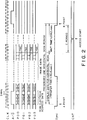
- the apparatus body 14 always watches the signal Sync to transfer display data when the signal Sync is LOW and does not effect transfer after transfer of data for one horizontal scanning when the signal Sync is HIGH. More specifically, referring to Figure 2, at an instant when the signal Sync is turned LOW, the A/D ⁇ signal is turned HIGH at a point A and then the control circuit 15 returns the Sync signal to HIGH during the display data transfer period. Then, at a point B which is one horizontal scanning period counted from the point A, the Sync signal is returned to LOW. If the apparatus body 14 successively transfers display data at the point B, i.e., if a subsequent scanning electrode is driven, the A/D ⁇ signal is again turned HIGH to start the transfer. Refresh drive or whole display picture (area) scanning drive is performed in this embodiment, so that the drive is continuously effected line-sequentially.
- the above-mentioned one horizontal scanning period (corresponding to one scanning selection period) is prescribed depending on the characteristic of the ferroelectric liquid crystal and the driving method in consideration also of optimum driving conditions.
- the one horizontal scanning period was set to about 250 ⁇ sec at room temperature so that the frame frequency was about 10 Hz.
- the transfer clock CLK frequency was 5 MHz, and the transfer time of the scanning electrode address data and image data was about 40.8 ⁇ sec, and the waiting time shown in Figure 2 was 209.2 ⁇ sec.
- the control signal CNT is a control signal for generating a desired driving waveform. This is supplied from the control circuit 15 to the respective drive circuits 12 and 13.
- the time for outputting CNT is the same as the time for outputting the scanning electrode address data A0 - A11 from the control circuit 15 to the scanning electrode drive circuit 12 and also the same as the time for transferring the image data in the shift register 13A to the line memory 13B.
- the time for outputting the CNT signal is switched at a point which is after the completion of the transfer time (40.8 ⁇ sec) from the low level-starting point (A point) of the Sync signal and one horizontal scanning period counted from the access starting point for the previous line.
- a C period set between the termination of the transfer time and the point (B) of a subsequent signal turning low is determined at constant.
- the above communication is effect between the drive circuits 12 and 13, and also between the apparatus body 14 and the control circuit 15, and the display panel is driven according to the above time-sequence.
- refreshing drive is performed by an interlaced scanning (jump-scanning) scheme as described below and partial rewriting drive is performed by a non-interlaced scanning (non-jump-scanning) scheme.
- a scanning selection signal is sequentially applied to the scanning electrodes with jumping of N lines apart (N ⁇ 1, preferably 4 ⁇ N ⁇ 20), in one vertical scanning period (corresponding to one field period), and one picture scanning (corresponding to one frame scanning) is effected by N+1 times of field scanning.
- N N lines apart
- one picture scanning corresponding to one frame scanning
- one vertical scanning is effected two or more scanning electrodes apart and scanning electrodes not adjacent to each other are selected (scanned) in at least two consecutive times of vertical scanning.
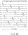
- Figure 3A shows a scanning selection signal S S , a scanning non-selection signal S N , a white data signal I W and a black data signal I B .
- Figure 3B shows a voltage waveform applied to a selected pixel among the pixels on a selected scanning electrode receiving a scanning selection signal (a voltage (I W -S S ) applied to a pixel receiving a white data signal I W ), a voltage waveform applied to a non-selected pixel on the same selected scanning electrode (a voltage (I B -S S ) applied to a pixel receiving a black data signal I B ), and voltage waveforms applied to two types of pixels on a non-selected scanning electrode receiving a scanning non-selection signal.
- a scanning selection signal a voltage (I W -S S ) applied to a pixel receiving a white data signal I W
- a voltage waveform applied to a non-selected pixel on the same selected scanning electrode a voltage (I B -S S ) applied to
- the pixels on a selected scanning electrode are simultaneously supplied with a voltage providing one orientation state of a ferroelectric liquid crystal to be erased into a black state based on such one orientation state of the ferroelectric liquid crystal (a pair of cross nicol polarizers are so arranged as to effect erasure into a black state in this embodiment, but it is also possible to arrange polarizers so as to cause erasure into a white state) in phase t1 regardless of the kind of a data signal supplied.
- the pixels on a scanning electrode receiving the scanning non-selection signal are supplied with voltages ⁇ V3 below the threshold voltage of the ferroelectric liquid crystal.
- a voltage of a polarity opposite to that of the data signal in the writing phase t2 is supplied from a data electrode.
- a pixel at the time of scanning non-selection is supplied with an AC voltage to improve the threshold characteristic of the ferroelectric liquid crystal.
- Such a signal applied through a data electrode is called an auxiliary signal and is explained in detail in U.S. Patent No. 4,655,561.
- Figure 3C is a time chart of voltage waveforms for providing a certain display state.
- a scanning selection signal is applied to the scanning electrodes three lines apart in one field, and one frame scanning (one picture scanning) is effected by 4 consecutive times of field scanning so that no adjacent pair of scanning electrodes are supplied with a scanning selection signal together in 4 consecutive fields.
- a scanning selection period ( t1 + t2 + t3 ) can be set longer as required at a low temperature, so that occurrence of flickering attributable to scanning drive at a low frame frequency can be remarkably suppressed even at such a low frame frequency as 5 - 10 Hz, for example.
- a scanning selection signal so that non-adjacent scanning electrodes are selected in consecutive four field scannings, an image flow can be effectively solved.
- FIG 3D shows an embodiment using driving waveforms shown in Figure 3A.
- the scanning electrodes are selected 5 lines (scanning electrodes) apart so that non-adjacent scanning electrodes are selected in 6 times of consecutive field scanning.
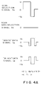
- FIGS 4A and 4B show another driving embodiment used in the present invention.
- Figure 4C is a time chart of voltage waveforms for providing a certain display state.
- a scanning selection signal is applied to the scanning electrodes with jumping of 4 lines apart in one field so as to complete one frame scanning in 5 fields.
- non-adjacent scanning electrodes are supplied with a scanning selection signal in consecutive 5 times of field scanning.
- the present invention is not restricted to the above-described embodiments but can be effected generally in such a manner that a scanning selection signal is applied to the scanning electrodes with jumping of one or more lines apart, preferably 4 - 20 lines apart.
- the peak values of the voltages V1, -V2 and ⁇ V3 may be set to satisfy the relation of
- the pulse durations of these voltage signals may be set to generally 1 ⁇ sec - 1 msec, preferably 10 ⁇ sec - 100 ⁇ sec, and may preferably be set to be longer at a lower temperature and shorter at a higher temperature.
- Partial rewriting may be performed by intermitting the above-mentioned whole display area scanning by refreshing drive in the present invention. Accordingly, some operational relationships between partial scanning of scanning electrodes used in the partial rewriting drive and the whole display picture scanning are set forth hereinbelow.
- Figure 5 shows a circuit structure for conducting a series of operations defined in the above paragraphs (1) - (6). More specifically, Figure 5 shows a detailed structure of the apparatus body 14 shown in Figure 1, which is functionally provided with a CPU unit 51, a VRAM unit 52 and a sequencer unit 53.
- the CPU unit constitutes a control center of the apparatus body 14 and functions as the instruction source of image data generation.
- the VRAM unit 52 comprises a VRAM 521 and a VRAM timing signal generator 522 and functions as a memory for storing image data.
- the sequencer unit 53 comprises a first address switch 531, a second address switch 532, a 400-line counter 533, a scanning counter (8-line counter) 534, a 50-line counter 535, a flag memory 536, a sequencer 537, an input/output port 538, and a 800-dot counter 539.
- the sequencer unit 53 controls the access of the CPU unit 51 to the VRAM unit 52 and also the VRAM unit 52 with respect to image data transfer to the display panel 11.
- a VA signal for access to an address in the VRAM 521 is an address signal selected from a BA signal, an ADR signal and an RA signal as follows:
- the above-mentioned BA signal, ADR signal and RA signal are subjected to selection by the first address switch 531 to be outputted as a VRAM address VA signal.
- the first address switch 531 is controlled by the sequencer circuit 537.
- the scanning counter 534 is a counter for defining a scanning scheme and counts the number of scanning lines in jump-scanning for the refreshing drive.
- the scanning lines are jump-scanned 7 lines apart.
- the 50-line counter 535 defines the number of scanning lines in one field of the refreshing drive.
- 400 scanning lines are jump-scanned 7 lines apart and are frame-scanned in 8 fields, so that 50 scanning lines are counted to make one field.
- the 400-line counter 533 counts a prescribed number of scanning lines (set to 400 lines in this embodiment) and functions as a frame counter in the whole display picture scanning. In the partial rewriting drive, the 400-line counter 533 generates scanning line address data for the partial scanning of scanning lines and causes an access to the VRAM address.
- the second address switch 532 is a circuit for selecting either one of the BA signal and ADR signal for access (FA) to the flag memory 536.
- the two kinds of the flag memory address signals are selected by the sequencer circuit 537.
- the flag memory 536 is a memory for allocating one bit of data for each scanning electrode.
- the one bit of data is hereinafter called a "flag".
- Flags are generated by writing an image data from the CPU 51 into the VRAM 521.
- VRAM address signals (ADR) generated at the time of rewriting by the CPU 51 into the VRAM 521 are sampled and converted into address signals (FA) each corresponding to one scanning electrode, based on which a flag of "0" or "1" is written in the flag memory 536.
- ADR VRAM address signals
- FA address signals
- the 200-dot counter 539 is a circuit for counting the amount of image data to be transferred in one horizontal scanning and controlling the input/output port 538.
- the input/output port 538 transfers the image data PD0, PD1, PD2, PD3, CLK and A/D ⁇ comprising scanning electrode address data and image data to the control circuit 15 and receives the Sync signal from the control circuit.
- Figure 6 is a flow chart showing an operational relationship between the whole display picture scanning drive and the partial rewriting scanning drive.
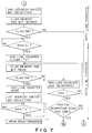
- Figure 7 is a flow chart of the partial rewriting scanning drive.
- Figure 8 is a flow chart of the whole display picture scanning drive.
- a VRAM address signal (RA) from the scanning counter 534 which is a counter for the whole display picture scanning drive and the 50-line counter 535 is supplied to the VRAM 521 as a scanning electrode address data VA.
- the scanning electrode address data VA and image data in the VRAM designated by the VA signal are read out-and transferred to the display panel 11.
- one increment is given to the 50-line counter 535. If the count is 49 at the time of the increment, the partial rewriting routine is started, and if the count is not 49, the "L" level of the Sync signal is again awaited.
- the partial rewriting routine is started and operated in the following manner.
- the count of 49 means that the display data to be subsequently sent are for a 49th-scanning electrode in one field, whereby the partial rewriting routine is started from terminal I shown in Figure 7. Further, even while the partial rewriting routine is operated, one field scanning drive is operated on the display panel, so that the time relation between the partial rewriting routine and the one-field scanning drive is shown by the notes of 49th LINE TRANSFER and 50th LINE TRANSFER in Figure 7.
- the transfer in the 49th LINE TRANSFER and 50th LINE TRANSFER refers to transfer of scanning electrode address data and image data from VRAM 521 in the one-field scanning drive.
- FA flag memory address signal
- the flag "1" means that rewriting is caused on a scanning electrode shown by a flat memory address (FA). In contrast thereto, no rewriting is indicated by the flag "0". The operation from the terminal I up to now is performed during the 49th-line transfer.
- the first address switch 531 is set to the position of BA-selection, and subsequent to the one-field scanning drive, the flag address held by the flag memory 536 is made the scanning electrode address for the partial rewriting scanning and image data in VRAM designated by the scanning electrode address are transferred. Further, simultaneously with the transfer, the above-mentioned operation after "400-LINE COUNTER ONE INCREMENT" is performed.
- the above operation with a flag "1" bit is repeated 400 times. Then, at the 400 times of repetition, i.e., after evaluating the value due to the increment, and then it is judged whether the 400 is given by the number of scanning for the partial rewriting scanning. When 400 is not reached, the operation goes to a terminal to return to the partial rewriting routine, and when 400 is reached, the operation goes to a terminal so as to proceed to the whole display picture scanning routine.
- the operation is started from a terminal a, and the RA signal is selected by the first address switch 531. Then, a Sync signal at "L" level is awaited, and when it is satisfied, the scanning electrode address data defined by the scanning counter 534 and the 50-line counter 535 and image data designated thereby in VRAM are transferred. Then, one increment is given to the 50-line counter 535. Then, the count given by the increment is judged to be whether it has reached 50, and if it is not 50, a subsequent transfer is performed. If the counter is 50, the one-field scanning drive is judged to be completed and one increment is given to the scanning counter 534 to set a next field. Then, the count in the counter 534 is judged whether it has reached 8.
- the above operation corresponds to the driving of the display panel as follows.
- the whole display picture scanning drive is always repeated.
- Search for image rewriting is effected for each one-field scanning drive.
- partial rewriting is performed after the completion of one-field scanning drive.
- the scanning drive in the partial rewriting is performed according to a non-interlaced mode.
- the system is automatically moved to one-field scanning drive according to an interlaced scanning mode.
- the display panel 11 is subjected to repetition of a series of operations as described above based on image data from the apparatus body.
- the BA signal and the RA signal are only temporarily selected by the first address switch 531, and otherwise the ADR signal from the CPU 51 is selected.
- the data in VRAM 521 are in a condition that the access thereto is always possible by the CPU 51.
- Figure 9 is a flow chart showing another partial rewriting routine used in the present invention
- Figure 10 is a flow chart showing a display operation including the partial rewriting. In the operation, it is judged whether new data have came from CPU, and if not, this operation is repeated. When new data appear, the previous data in VRAM are rewritten. Thus, the apparatus body 14 adds scanning electrode address data to the image data from CPU and transfer the sum to the control circuit 15.
- the whole display scanning drive is executed at definite intervals.
- the main program is interrupted on demand for the whole display picture scanning drive, and the apparatus body 14 executes the routine shown in Figure 10 at definite intervals according to the interruption demand.
- the apparatus body 14 executes the routine shown in Figure 10 at definite intervals according to the interruption demand.
- the partial rewriting is under operation, it is interrupted to refuse new data from CPU.
- image data for the whole picture are transferred to the control circuit 15.
- a time until the subsequent whole display picture scanning drive is set (to 1 second in this embodiment). Then, new data from CPU are received.
- the operation of the apparatus body 14 is defined in the above described manner to effect the driving method according to the present invention.
- Figures 11A and 11B show time charts for showing the display operation principle according to the present invention, wherein the first frame is a period for the whole display picture scanning drive. If rewriting data are generated during this period, the apparatus body 14 prepares rewriting data (generates scanning electrode address data and image data serially) in the above described manner. Then, at the beginning of the second frame, the partial rewriting is started according to the routine shown in Figures 9 and 10. After the completion of the partial rewriting and on reaching a prescribed definite time, the whole display picture scanning drive is resumed.
- the whole display picture scanning drive is started as soon as the partial rewriting is completed and a definite time is reached as shown in Figure 11A.
- the partial rewriting is interrupted to proceed to the subsequent whole display picture scanning drive when the number of scanning for the partial rewriting exceeds 400.
- the whole display picture scanning drive cycle has been set to 1 second.
- Figure 12 is an example of a multi-window picture display.
- the hole display picture comprises respectively different pictures in various display regions.
- a window 1 shows a picture of a categorized total result expressed in a circle.
- a window 2 shows the categorized total at the window 1 expressed in a table.
- a window 3 shows the categorized total at the window 1 expressed in a bar graph.
- a window 4 shows characters relating to formation of sentences.
- the back ground is formed in plain white.
- the window 4 constitutes a picture in operation and the other pictures are in a still picture state.
- the window 4 is under preparation of a sentence and in a motion picture state.
- the motion picture state may specifically include motions, such as scrolling; insertion, deletion and copying of words and paragraphs; and regional transfer. These motions generally require a quick movement. More specific display operation examples are given hereinbelow.
- One character is additionally displayed in an arbitrary row in the window 4.
- a character font is assumed to be composed of 16x16 dots.
- the additional display of one character corresponds to rewriting of 16 scanning electrodes.
- only 16 scanning electrodes are rewritten as follows during the whole display picture scanning. First of all, search of the flag memory 536 is started from the 49th line in a field in which one character is additionally rewritten in VRAM 521 by CPU 51 and the search is continued until 16 bits of flags "ON" are detected to partially rewrite only 16 scanning electrodes after completing the field scanning drive under way. Then, a subsequent field scanning drive is sequentially effected from a leading scanning electrode.
- one horizontal scanning time is assumed to be 250 ⁇ sec
- a partial scanning drive of scanning electrodes corresponding to a font given by a cursor or mouse may be repeated cyclically for different scanning electrodes to afford a moving display by such a cursor or mouse at a very high speed.
- the timing for switching from the whole display picture scanning drive to the partial rewriting scanning drive is the same as in the above-mentioned first example.
- the partial rewriting is replaced by a whole display picture rewriting scanning, so that the number of scanning electrodes to be scanned for rewriting amounts to 400.
- 400 scanning electrodes are scanned by the non-interlaced scanning mode to rewrite the whole picture, and in a subsequently frame, the whole picture is scanned by the interlaced scanning mode.
- the display picture is rewritten alternately by the non-interlaced scanning mode and the interlaced scanning mode.
- image data transferred from VRAM comprise newest image data even in the interlaced scanning mode.
- a window 4 is subjected to smooth scrolling according to the routine shown in Figures 9 - 11.
- the smooth scrolling display corresponds to rewriting of 200 scanning electrodes.
- FIG. 13 schematically illustrates an embodiment of a ferroelectric liquid crystal cell which comprises a pair of electrode plates (glass substrates coated with transparent electrodes) 131A and 131B and a layer of ferroelectric liquid crystal having molecular layers 132 disposed between and perpendicular to the electrode plates.
- the ferroelectric liquid crystal assumes chiral smectic C phase or H phase and is disposed in a thickness (e.g., 0.5 - 5 microns) thin enough to release the helical structure inherent to the chiral smectic phase.
- liquid crystal molecules 133 are oriented to the electric field.
- a liquid crystal molecule has an elongated shape and shows a refractive anisotropy between the long axis and the short axis. Therefore, if the cell is sandwiched between a pair of cross nicol polarizers (not shown), there is provided a liquid crystal modulation device.
- a liquid crystal molecules 133 is oriented to a first orientation state 133A.
- the liquid crystal molecule 133 is oriented to a second orientation state 133B to change its molecular direction. Further, the respective orientation states are retained as far as an electric field E or -E applied thereto does not exceed a certain threshold.
- the ferroelectric liquid crystal device used in this embodiment has an inclination of monostability so that the first stable state 133A and second stable state 133B are unsymmetrical. As a result, the liquid crystal molecules tend to be oriented to either one of the orientation states or to another stabler third orientation state.
- the present invention is suitably applied to such a ferroelectric liquid crystal device having an inclination of monostability but can also be applied to a ferroelectric liquid crystal device in an alignment state showing semipermanent or permanent bistability as disclosed by U.S. Patent No. 4,367,924 or a ferroelectric liquid crystal device in an alignment state retaining a helical structure.
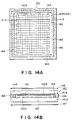
- Figure 14A and 14B illustrate an embodiment of the liquid crystal device according to the present invention.
- Figure 14A is a plan view of the embodiment and
- Figure 14B is a sectional view taken along the line A-A in Figure 14A.
- a cell structure 140 shown in Figure 14 comprises a pair of substrates 141A and 141B made of glass plates or plastic plates which are held with a predetermined gap with spacers 144 and sealed with an adhesive 146 to form a cell structure.
- an electrode group e.g., an electrode group for applying scanning voltages of a matrix electrode structure
- a predetermined pattern e.g., of a stripe pattern.
- another electrode group e.g., an electrode group for applying signal voltages of the matrix electrode structure
- a plurality of transparent electrodes 142B intersecting with the transparent electrodes 142A.
- an alignment control film 145 composed of an inorganic insulating material such as silicon monoxide, silicon dioxide, aluminum oxide, zirconia, magnesium fluoride, cerium oxide, cerium fluoride, silicon nitride, silicon carbide, and boron nitride, or an organic insulating material such as polyvinyl alcohol, polyimide, polyamide-imide, polyester-imide, polyparaxylylene, polyester, polycarbonate, polyvinyl acetal, polyvinyl chloride, polyamide, polystyrene, cellulose resin, melamine resin, urea resin and acrylic resin.
- an inorganic insulating material such as silicon monoxide, silicon dioxide, aluminum oxide, zirconia, magnesium fluoride, cerium oxide, cerium fluoride, silicon nitride, silicon carbide, and boron nitride
- an organic insulating material such as polyvinyl alcohol, polyimide, polyamide-imide, polyester-imide, polyparaxyly
- the alignment control film 145 may be formed by first forming a film of an inorganic insulating material or an organic insulating material as described above and then rubbing the surface thereof in one direction with velvet, cloth, paper, etc.
- the alignment control film 145 may be formed as a film of an inorganic insulating material such as SiO or SiO2 on the substrate 141B by the oblique or tilt vapor deposition.
- the surface of the substrate 141B of glass or plastic per se or a film of the above-mentioned inorganic material or organic material formed on the substrate 141B is subjected to oblique etching to provide the surface with an alignment control effect.
- the alignment control film 145 also functions as an insulating film.
- the alignment control film may preferably have a thickness in the range of 100 ⁇ to 1 micron, especially 500 to 5000 ⁇ .
- the insulating film also has a function of preventing the occurrence of an electric current which is generally caused due to minor quantities of impurities contained in the liquid crystal layer 143, whereby deterioration of the liquid crystal compounds is prevented even on repeating operations.
- ferroelectric liquid crystal 143 a liquid crystal compound or composition as disclosed in U.S. Patent Nos. 4561726, 4614609, 4589996, 4592858, 4596667, 4613209, etc., may be used.
- the device shown in Figures 14A and 14B further comprises polarizers 143 and 148 having polarizing axes crossing each other, preferably at 90 degrees.
- a partial rewriting scanning drive and a whole display picture scanning drive are compatible realized, and further a partial motion picture at a low frame frequency can be effected at a high speed while a still picture display is stably effected by using a ferroelectric liquid crystal material having a strong inclination of monostability.
- a display apparatus comprises (a) a display panel having a display picture area formed by scanning electrodes and data electrodes arranged in a matrix; (b) drive means including a first means for driving the scanning electrodes and a second means for driving the data electrodes; and (c) control means for controlling the drive means so as to repeat a partial rewriting scanning drive comprising applying an scanning selection signal to only a part of the scanning electrodes forming the display picture area.
Abstract
Description
- The present invention relates to a display apparatus, particularly a ferroelectric liquid crystal display apparatus suitable for moving display using a cursor, mouse, etc.
- For a CRT (cathode ray tube) wherein an image is formed by utilizing persistence on a fluorescent screen and a TN-type LCD (twisted nematic-type liquid crystal device) wherein an image is formed by utilizing a transmittance change depending on an effective value of driving voltage, it is necessary to use a sufficiently high frame frequency which is a frequency required for forming one picture based on their display principle. The required frame frequency is generally considered to be 30 Hz or higher. The frame frequency is expressed as the reciprocal of the product of a number of scanning lines and a horizontal scanning time for scanning each scanning line. The scanning processes or modes known at present include the interlaced scanning process (with jumping of one or more lines apart) and the non-interlaced scanning process. Other practical scanning processes may include the pairing process and a process comprising simultaneous and parallel scanning of divided portions of a picture screen, while the latter process is restricted to LCD. The NTSC standard system has adopted an interlaced scanning process comprising a 2 fields/frame and a frame frequency of 30 Hz, wherein the horizontal scanning time is about 63.5 µsec and the number of scanning lines is about 480 (for constituting effective display area). The TN-type LCD has generally adopted a non-interlaced system including 200 - 400 scanning lines and a frame frequency of 30 Hz or higher. Further, for CRT, there has been also adapted a non-interlaced scanning system using a frame frequency of 40 - 60 Hz and 200 - 1000 scanning lines.
- Now, it is assumed to drive a CRT or TN-type LCD comprising 1920 (number of scanning lines) x 2560 pixels. In the case of an interlaced system using a frame frequency of 30 Hz, the horizontal scanning time is about 17.5 µsec and the horizontal dot clock frequency is about 147 MHz (without consideration of horizontal flyback for CRT). In the case of CRT, the horizontal dot clock frequency of 147 MHz leads to a very high beam scanning speed which exceeds by far the maximum electron beam modulation frequency of a beam gun used in picture tubes available at present, so that accurate image formation cannot be effected even by scanning at 17.5 µsec. In the case of TN-type LCD, driving of 1920 scanning lines corresponds to a duty factor of 1/1920 which is much lower than the minimum duty factor of about 1/400 available at present, so that displaying is failed. On the other hand, if driving at a practical horizontal scanning time is considered, the frame frequency becomes lower than 30 Hz so that the scanning state is visually observed and flickering is caused to remarkably impair the display quality. In this way, the enlargement and densification of a picture for CRT and TN-type LCD has been restricted so far because the number of scanning lines cannot be sufficiently increased because of restriction by the display principles and driving elements.
- On the other hand, in recent years, Clark and Lagerwall have proposed a ferroelectric liquid crystal device having both a high-speed responsive characteristic and a memory characteristic (bistability).
- The ferroelectric liquid crystal device shows a chiral smectic C phase (SmC*) or H phase (SmH*) in a specific temperature range, and in this state, shows a bistability, i.e., property of assuming either a first optically stable state or a second optically stable state depending on an applied electric field and retaining the resultant state in the absence of an electric field applied thereto. Further, the ferroelectric liquid crystal device shows a quick response to a change in electric field and is therefore expected to be widely used as a display device of a high speed and memory-type.
- However, it is generally difficult for such a ferroelectric liquid crystal device to show an ideal bistability as proposed by Clark et al but it is liable to show a monostability. Clark et al used an alignment control method, such as application of a shearing force by relative movement or application of a magnetic field in order to realize a permanent bistability. From the viewpoint of production technique, however, it is advantageous to apply uniaxial orientation treatment, such as rubbing or oblique vapor deposition to a substrate. Such a uniaxial orientation treatment applied to a substrate for alignment control has sometimes failed to provide a permanent bistability. In the resultant alignment state failing to provide a permanent bistability, i.e., a so-called monostable alignment state, a biaxial orientation state formed under application of electric fields tends to be transformed into a uniaxial orientation state under no electric field in a period ranging from several milliseconds to several hours. For this reason, a display apparatus using such a ferroelectric liquid crystal device showing monostability has involved a problem that an image formed under application of electric fields is lost in accordance with the removal of the electric fields. Particularly in a multiplexing drive, there has been observed a problem that written states in pixels on non-addressed scanning lines are gradually lost.
- In order to solve such a problem, there has been proposed a driving scheme (refreshing drive scheme) wherein pixels on a selected scanning line are selectively supplied with a voltage for providing "black" or a voltage for providing "white", the scanning lines are sequentially selected in a cycle of one frame or one field, and the cycle is repeated for writing. Such a refreshing drive scheme provides very little fluctuation in transmittance and has obviated difficulties, such as visual recognition of a writing scanning line (where a higher luminance than the other lines can be easily recognized) and occurrence of flickering under a frame frequency lower than 30 Hz. According to our study, a similar effect has been confirmed even under a low frequency as low as about 5 Hz.
- The above facts can be effectively utilized to solve altogether the problems against enlargement and densification of picture arising from the abovementioned essential requirement of CRT and TN-type LCD that a frame frequency of 30 Hz or higher is required for driving.
- However, such a low-frequency refreshing drive as described above is too slow for so-called motion picture display, such as smooth scrolling or cursor movement in character compiling or on a graphic display, thus resulting in deterioration of display performances. In recent years, there have been remarkable developments in computers, peripheral circuits thereof and softwares therefor. For example, for a large picture and high density display, there has been spread a display scheme called a multi-window display scheme, wherein a plurality of pictures are displayed in superposition in a display area. A display apparatus incorporating a ferroelectric liquid crystal device is one which can afford to provide enlargement and densification of a picture area which exceeds by far those realized by conventional display apparatus, such as CRT and TN-type LCD. In accordance with such enlargement and densification, there arise problems that the frame frequency is lowered, and the velocity of smooth scrolling and cursor movement is lowered even further.
- An object of the present invention is to provide a display apparatus having solved the above-described problems, particularly to provide a display apparatus capable of a high-speed cursor movement and mouse movement under scanning drive at a low frame frequency as low as 30 Hz or below.
- According to a principal aspect of the present invention, there is provided a display apparatus, comprising:
- (a) a display panel having a display picture area formed by scanning electrodes and data electrodes arranged in a matrix;
- (b) drive means including a first means for driving the scanning electrodes and a second means for driving the data electrodes; and
- (c) control means for controlling the drive means so as to repeat a partial rewriting scanning drive comprising applying an scanning selection signal to only a part of the scanning electrodes forming the display picture area.
- According to a second aspect of the present invention, there is provided a display apparatus, comprising:
- (a) a display panel having a display picture area formed by scanning electrodes and data electrodes arranged in a matrix;
- (b) drive means including a first means for driving the scanning electrodes and a second means for driving the data electrodes; and
- (c) control means for controlling the drive means so as to scan-select the scanning electrodes with jumping of one or more scanning electrodes apart for one vertical scanning drive of the scanning electrodes constituting the whole picture area and scan-select the scanning electrodes without jumping for scanning drive of only a part of the scanning electrodes constituting the whole picture area.
- According to a third aspect of the present invention, there is provided a display apparatus comprising:
- (a) a display panel having a display picture area formed by scanning electrodes and data electrodes arranged in a matrix;
- (b) drive means including a first means for driving the scanning electrodes and a second means for driving the data electrodes; and
- (c) control means for controlling the drive means so as to scan-select the scanning electrodes with jumping of two or more scanning electrodes apart in one vertical scanning and scan-select non-adjacent scanning electrodes in at least two consecutive times of vertical scanning for scanning drive of the scanning electrodes constituting the whole picture area, and scan-select the scanning electrodes without jumping for scanning drive of only a part of the scanning electrodes constituting the whole picture area.
- These and other objects, features and advantages of the present invention will become more apparent upon a consideration of the following description of the preferred embodiments of the present invention taken in conjunction with the accompanying drawings.
-
- Figure 1 is a block diagram of a display apparatus according to the invention;
- Figure 2 is a time chart showing time correlation between signal transfer and driving;
- Figures 3A - 3D and Figures 4A - 4C respectively show a set of driving signal waveforms used in the invention;
- Figure 5 is a block diagram of an apparatus body;
- Figure 6 is a flow chart showing an operation routine for whole display picture scanning drive and partial rewriting scanning drive; Figure 7 is a flow chart showing an operation routine for partial rewriting scanning drive; Figure 8 is a flow chart showing one frame scanning drive;
- Figure 9 is a flow chart showing a partial rewriting routine; Figure 10 is a whole display picture scanning drive routine;
- Figure 11A is a time table for a case where the number of scanning electrodes for partial rewriting scanning < the number of whole picture scanning electrodes; Figure 11B is a time chart for a case where the number of scanning electrodes for partial rewriting scanning ≧ the number of whole picture scanning electrodes;
- Figure 12 is an illustration of an example of display image used in the invention;
- Figure 13 is a schematic perspective view for illustrating a ferroelectric liquid crystal device used in the invention;
- Figure 14A is a plan view of a device used in the invention; and Figure 14B is a sectional view taken along the line A-A in Figure 14A.
- Figure 1 is a block diagram of a display apparatus according to the present invention showing an arrangement of a liquid crystal display apparatus and an apparatus body for supplying display data signals.
- A display panel 11 comprises a matrix electrode structure composed of 400
scanning electrodes data electrodes 13D between which a ferroelectric liquid crystal is disposed. Thescanning electrodes 12C are connected to a scanningelectrode drive circuit 12 and the data electrode 12D are connected to a data electrode drive circuit 13. The scanningelectrode drive circuit 12 is provided with adecoder 12A and anoutput stage 12B. The data electrode drive circuit 13 is provided with ashift register 13A, a line memory 13B and anoutput stage 13C. - First of all, scanning electrode address data for addressing
scanning electrodes 12C and image data are supplied from anapparatus body 14 to a control circuit through four signal lines PD0, PD1, PD2 and PD3. In this embodiment, scanning electrode address data (A0, A1, A2, ..., A11) and image data (D0, D1, D2, D3, ..., D798, D799) are transferred respectively through the same transmission signal lines PD0 - PD4, so that it is necessary to differentiate the scanning electrode address data and the image data. In this embodiment, a discriminating signal A/D⁻ is used. The A/D⁻ signal at a high level means scanning electrode address data, and the A/D⁻ signal at a low level means image data. The A/D⁻ signal also contains a meaning of a transfer-initiation signal for transfer of display data. - When scanning electrode address data are supplied to the scanning
electrode drive circuit 12 and image data are supplied to the data electrode drive circuit 13, the scanning electrode address data A0 - A11 and the image data D0 - D799 are serially supplied through the signal lines PD0 - PD3. It is necessary to provide a circuit for distributing the scanning electrode address data A0 - A11 and the image data D0 - D799 or extracting the scanning electrode address data A0 - A11. This operation is performed by thecontrol circuit 15. Thecontrol circuit 15 extracts the scanning electrode address data A0 - A11 supplied through the signal lines PD0 - PD3, temporarily stores the data and supplies the data to the scanningelectrode drive circuit 12 in a horizontal scanning period for driving a designatedscanning electrode 12C. The scanning electrode address data A0 - A11 are supplied to thedecoder 12A in the scanningelectrode drive circuit 12 and select ascanning electrode 12C through thedecoder 12A. - On the other hand, the image data D0 - D799 are supplied to the
shift register 13A in the data electrode drive circuit 13 and separated into image data D0 - D799 for pixels corresponding to thedata electrodes 13D (800 lines) while being shifted for 4 pixels each by transfer clock signals CLK. When a shifting operation of the data for one horizontal scanning line is completed by theshift register 13, 800 bits of the image data D0 - D799 in the shift register 13 are transferred to the line memory 13B and memorized therein in a horizontal scanning period. Further, in this embodiment, the drive of the display panel 11 and the generation of the scanning electrode address data A0 - A11 and image data D0 - D799 in theapparatus body 14 are not synchronized, so that it is necessary to synchronize thecontrol circuit 15 and theapparatus body 14 at the time of display data transfer. For this purpose, a synchronizing signal Sync is generated in the control circuit for each horizontal scanning. - The signal Sync is associated with the signal A/D⁻. The
apparatus body 14 always watches the signal Sync to transfer display data when the signal Sync is LOW and does not effect transfer after transfer of data for one horizontal scanning when the signal Sync is HIGH. More specifically, referring to Figure 2, at an instant when the signal Sync is turned LOW, the A/D⁻ signal is turned HIGH at a point A and then thecontrol circuit 15 returns the Sync signal to HIGH during the display data transfer period. Then, at a point B which is one horizontal scanning period counted from the point A, the Sync signal is returned to LOW. If theapparatus body 14 successively transfers display data at the point B, i.e., if a subsequent scanning electrode is driven, the A/D⁻ signal is again turned HIGH to start the transfer. Refresh drive or whole display picture (area) scanning drive is performed in this embodiment, so that the drive is continuously effected line-sequentially. - The above-mentioned one horizontal scanning period (corresponding to one scanning selection period) is prescribed depending on the characteristic of the ferroelectric liquid crystal and the driving method in consideration also of optimum driving conditions. In this embodiment, the one horizontal scanning period was set to about 250 µsec at room temperature so that the frame frequency was about 10 Hz. Further, the transfer clock CLK frequency was 5 MHz, and the transfer time of the scanning electrode address data and image data was about 40.8 µsec, and the waiting time shown in Figure 2 was 209.2 µsec. The control signal CNT is a control signal for generating a desired driving waveform. This is supplied from the
control circuit 15 to therespective drive circuits 12 and 13. The time for outputting CNT is the same as the time for outputting the scanning electrode address data A0 - A11 from thecontrol circuit 15 to the scanningelectrode drive circuit 12 and also the same as the time for transferring the image data in theshift register 13A to the line memory 13B. - The time for outputting the CNT signal is switched at a point which is after the completion of the transfer time (40.8 µsec) from the low level-starting point (A point) of the Sync signal and one horizontal scanning period counted from the access starting point for the previous line. In this embodiment, a C period set between the termination of the transfer time and the point (B) of a subsequent signal turning low is determined at constant.
- The above communication is effect between the
drive circuits 12 and 13, and also between theapparatus body 14 and thecontrol circuit 15, and the display panel is driven according to the above time-sequence. - In the present invention, refreshing drive is performed by an interlaced scanning (jump-scanning) scheme as described below and partial rewriting drive is performed by a non-interlaced scanning (non-jump-scanning) scheme.
- A scanning selection signal is sequentially applied to the scanning electrodes with jumping of N lines apart (N ≧ 1, preferably 4 ≦ N ≦ 20), in one vertical scanning period (corresponding to one field period), and one picture scanning (corresponding to one frame scanning) is effected by N+1 times of field scanning. In the present invention, it is particularly preferred that one vertical scanning is effected two or more scanning electrodes apart and scanning electrodes not adjacent to each other are selected (scanned) in at least two consecutive times of vertical scanning.
- Figure 3A shows a scanning selection signal SS, a scanning non-selection signal SN, a white data signal IW and a black data signal IB. Figure 3B shows a voltage waveform applied to a selected pixel among the pixels on a selected scanning electrode receiving a scanning selection signal (a voltage (IW-SS) applied to a pixel receiving a white data signal IW), a voltage waveform applied to a non-selected pixel on the same selected scanning electrode (a voltage (IB-SS) applied to a pixel receiving a black data signal IB), and voltage waveforms applied to two types of pixels on a non-selected scanning electrode receiving a scanning non-selection signal. According to Figures 3A and 3B, the pixels on a selected scanning electrode are simultaneously supplied with a voltage providing one orientation state of a ferroelectric liquid crystal to be erased into a black state based on such one orientation state of the ferroelectric liquid crystal (a pair of cross nicol polarizers are so arranged as to effect erasure into a black state in this embodiment, but it is also possible to arrange polarizers so as to cause erasure into a white state) in phase t₁ regardless of the kind of a data signal supplied. in a subsequent phase t₂, a selected pixel on the selected scanning electrode (IW-SS) is supplied with a voltage (V₂+V₃) providing a white state based on the other orientation state of the ferroelectric liquid crystal, and the other pixels on the selected scanning electrode (IB-SS) are supplied with a voltage (

- Further, in this embodiment, in a phase t₃, a voltage of a polarity opposite to that of the data signal in the writing phase t₂ is supplied from a data electrode. As a result, a pixel at the time of scanning non-selection is supplied with an AC voltage to improve the threshold characteristic of the ferroelectric liquid crystal. Such a signal applied through a data electrode is called an auxiliary signal and is explained in detail in U.S. Patent No. 4,655,561.
- Figure 3C is a time chart of voltage waveforms for providing a certain display state. In this embodiment, a scanning selection signal is applied to the scanning electrodes three lines apart in one field, and one frame scanning (one picture scanning) is effected by 4 consecutive times of field scanning so that no adjacent pair of scanning electrodes are supplied with a scanning selection signal together in 4 consecutive fields. As a result, a scanning selection period (

- Figure 3D shows an embodiment using driving waveforms shown in Figure 3A. In this embodiment, the scanning electrodes are selected 5 lines (scanning electrodes) apart so that non-adjacent scanning electrodes are selected in 6 times of consecutive field scanning.
- Figures 4A and 4B show another driving embodiment used in the present invention.
- According to Figures 4A and 4B, on a scanning electrode receiving a scanning selection signal SS, all or a prescribed part of the pixels are simultaneously supplied with a voltage for erasure into a black state in phase


- Figure 4C is a time chart of voltage waveforms for providing a certain display state. According to the embodiment shown in Figure 4C, a scanning selection signal is applied to the scanning electrodes with jumping of 4 lines apart in one field so as to complete one frame scanning in 5 fields. Also in this embodiment, non-adjacent scanning electrodes are supplied with a scanning selection signal in consecutive 5 times of field scanning.
- The present invention is not restricted to the above-described embodiments but can be effected generally in such a manner that a scanning selection signal is applied to the scanning electrodes with jumping of one or more lines apart, preferably 4 - 20 lines apart. Further, in the present invention, the peak values of the voltages V₁, -V₂ and ±V₃ may be set to satisfy the relation of


- Partial rewriting may be performed by intermitting the above-mentioned whole display area scanning by refreshing drive in the present invention. Accordingly, some operational relationships between partial scanning of scanning electrodes used in the partial rewriting drive and the whole display picture scanning are set forth hereinbelow.
- (1) When a demand of rewriting a part of a display picture occurs during a whole display picture scanning by refreshing drive, the field scanning at the time of the occurrence is finished and then a partial scanning of scanning electrodes is performed.
- (2) The partial rewriting drive by partial scanning of scanning electrodes is performed by a non-interlaced scanning mode.
- (3) The maximum number of scanning lines for the partial scanning of scanning electrodes is set equal to the number of the total scanning lines constituting the whole display picture area (the number of scanning lines for one frame scanning). In other words, at a point of time when the number of scanning lines for partial scanning exceeds the number of scanning lines for the whole display picture scanning, the partial scanning of scanning lines is interrupted to resume the whole display picture scanning.
- (4) When a partial scanning of scanning lines is terminated while the number of scanning lines for the partial scanning is fewer than the maximum number of scanning lines for the partial scanning defined in the above paragraph (3), the field scanning drive is resumed from a first scanning line for a field scanning which is subsequent to the field scanning effected immediately before the partial scanning of scanning lines.
- (5) Image data rewriting for the VRAM (memory for image data storage) does not depend on the rewriting speed of the display panel.
- (6) Image data transferred to the display panel during the whole display picture scanning are those at the time of being transferred.
- Figure 5 shows a circuit structure for conducting a series of operations defined in the above paragraphs (1) - (6). More specifically, Figure 5 shows a detailed structure of the
apparatus body 14 shown in Figure 1, which is functionally provided with aCPU unit 51, aVRAM unit 52 and asequencer unit 53. - The CPU unit constitutes a control center of the
apparatus body 14 and functions as the instruction source of image data generation. - The
VRAM unit 52 comprises aVRAM 521 and a VRAMtiming signal generator 522 and functions as a memory for storing image data. - The
sequencer unit 53 comprises afirst address switch 531, asecond address switch 532, a 400-line counter 533, a scanning counter (8-line counter) 534, a 50-line counter 535, aflag memory 536, asequencer 537, an input/output port 538, and a 800-dot counter 539. Thesequencer unit 53 controls the access of theCPU unit 51 to theVRAM unit 52 and also theVRAM unit 52 with respect to image data transfer to the display panel 11. - A VA signal for access to an address in the
VRAM 521 is an address signal selected from a BA signal, an ADR signal and an RA signal as follows: - (1) BA signal: A VRAM address signal for access to a partial rewriting drive of the display panel 11.
- (2) ADR signal: A VRAM address signal at the time of image data generation from
CPU 51. - (3) RA signal: A VRAM address signal for access to a whole display picture scanning drive of the display panel.
- The above-mentioned BA signal, ADR signal and RA signal are subjected to selection by the
first address switch 531 to be outputted as a VRAM address VA signal. Thefirst address switch 531 is controlled by thesequencer circuit 537. - The
scanning counter 534 is a counter for defining a scanning scheme and counts the number of scanning lines in jump-scanning for the refreshing drive. In this embodiment, the scanning lines are jump-scanned 7 lines apart. - The 50-
line counter 535 defines the number of scanning lines in one field of the refreshing drive. In this embodiment, 400 scanning lines are jump-scanned 7 lines apart and are frame-scanned in 8 fields, so that 50 scanning lines are counted to make one field. The 400-line counter 533 counts a prescribed number of scanning lines (set to 400 lines in this embodiment) and functions as a frame counter in the whole display picture scanning. In the partial rewriting drive, the 400-line counter 533 generates scanning line address data for the partial scanning of scanning lines and causes an access to the VRAM address. - The
second address switch 532 is a circuit for selecting either one of the BA signal and ADR signal for access (FA) to theflag memory 536. The two kinds of the flag memory address signals are selected by thesequencer circuit 537. - The
flag memory 536 is a memory for allocating one bit of data for each scanning electrode. The one bit of data is hereinafter called a "flag". Flags are generated by writing an image data from theCPU 51 into theVRAM 521. VRAM address signals (ADR) generated at the time of rewriting by theCPU 51 into theVRAM 521 are sampled and converted into address signals (FA) each corresponding to one scanning electrode, based on which a flag of "0" or "1" is written in theflag memory 536. Thus, the location of scanning electrodes is detected based on the writing of image data by theCPU 51, and the detected data are written in theflag memory 536 as flags. Then, in the partial rewriting drive of the display panel 11, the flag data in theflat memory 536 and the BA signals from the 400-line counter 533 are compared, and the flag of "0" (= "OFF") or "1" (= "ON") is examined to designate only the scanning lines for the partial rewriting drive. - The 200-
dot counter 539 is a circuit for counting the amount of image data to be transferred in one horizontal scanning and controlling the input/output port 538. In this embodiment, 800 dots of data are transferred in 4 bits (PD0, PD1, PD2, PD3), so that 200 (= 800/4) counts is set. - The input/
output port 538 transfers the image data PD0, PD1, PD2, PD3, CLK and A/D⁻ comprising scanning electrode address data and image data to thecontrol circuit 15 and receives the Sync signal from the control circuit. - Figure 6 is a flow chart showing an operational relationship between the whole display picture scanning drive and the partial rewriting scanning drive. Figure 7 is a flow chart of the partial rewriting scanning drive. Figure 8 is a flow chart of the whole display picture scanning drive.
- Referring to Figures 5 and 6, first of all, as indicated by "1st ADDRESS SWITCH, RA SELECTION", a VRAM address signal (RA) from the
scanning counter 534 which is a counter for the whole display picture scanning drive and the 50-line counter 535 is supplied to theVRAM 521 as a scanning electrode address data VA. Then, on receiving the "L" level of the Sync signal, the scanning electrode address data VA and image data in the VRAM designated by the VA signal are read out-and transferred to the display panel 11. Then, one increment is given to the 50-line counter 535. If the count is 49 at the time of the increment, the partial rewriting routine is started, and if the count is not 49, the "L" level of the Sync signal is again awaited. Up to now, the operation of a so-called one-field scanning drive has been explained. - Then, when the count reaches 49, the partial rewriting routine is started and operated in the following manner.
- The count of 49 means that the display data to be subsequently sent are for a 49th-scanning electrode in one field, whereby the partial rewriting routine is started from terminal Ⓘ shown in Figure 7. Further, even while the partial rewriting routine is operated, one field scanning drive is operated on the display panel, so that the time relation between the partial rewriting routine and the one-field scanning drive is shown by the notes of 49th LINE TRANSFER and 50th LINE TRANSFER in Figure 7. The transfer in the 49th LINE TRANSFER and 50th LINE TRANSFER refers to transfer of scanning electrode address data and image data from
VRAM 521 in the one-field scanning drive. - As shown by "2nd ADDRESS SWITCH, BA-SELECTION", a flag memory address signal (FA) from the 400-
line counter 533 is supplied to theflag memory 536, and according to 400 times of counting, 400 bits of data in theflag memory 536 are read out. If a data with a flat "1" (= "ON") is present among the data thus read out, the partial rewriting routine is started thereafter. If the flag is "0" (= "OFF"), the operation proceeds to a terminal , i.e., returns to the whole display picture scanning drive. After the completion of the partial rewriting routine, one increment is given to the
scanning counter 534, and another RA signal is set to again perform a one-field scanning drive. - Herein, the flag "1" means that rewriting is caused on a scanning electrode shown by a flat memory address (FA). In contrast thereto, no rewriting is indicated by the flag "0". The operation from the terminal Ⓘ up to now is performed during the 49th-line transfer.
- Then, the operation in case where a bit with a flag "1" is present, will now be explained. When the 50th line transfer is started on receiving Sync = "L", the 400-line counter is first cleared (into "0"), one bit is read out from the
flag memory 536. The readout is effected from the first scanning electrode. Here, again the flag memory is checked whether "1" or "0". If "0", one increment is given to the 400-line counter, and another address signal (FA) is set for a subsequent 1-bit readout. At this time, when the count does not reach 400 as a result of the increment, one bit is read out from theflag memory 536. The operation up to now is repeated until a bit with a flag "1" is encountered. - When a bit with a flag "1" is read out, the operation of the 400-
line counter 533 is interrupted, the address of the flag "1" bit is retained. Under the condition of the operation of the 400-line counter 533 being interrupted; the completion of one field scanning drive is waited for by awaiting a Sync signal at "L" level. - On the other hand, the
first address switch 531 is set to the position of BA-selection, and subsequent to the one-field scanning drive, the flag address held by theflag memory 536 is made the scanning electrode address for the partial rewriting scanning and image data in VRAM designated by the scanning electrode address are transferred. Further, simultaneously with the transfer, the above-mentioned operation after "400-LINE COUNTER ONE INCREMENT" is performed. - The above operation with a flag "1" bit is repeated 400 times. Then, at the 400 times of repetition, i.e., after evaluating the value due to the increment, and then it is judged whether the 400 is given by the number of scanning for the partial rewriting scanning. When 400 is not reached, the operation goes to a terminalto return to the partial rewriting routine, and when 400 is reached, the operation goes to a terminal
 so as to proceed to the whole display picture scanning routine.
 - Next, the operation in the whole display picture scanning is explained.
- Referring to Figure 8, the operation is started from a terminal ⓐ, and the RA signal is selected by the
first address switch 531. Then, a Sync signal at "L" level is awaited, and when it is satisfied, the scanning electrode address data defined by thescanning counter 534 and the 50-line counter 535 and image data designated thereby in VRAM are transferred. Then, one increment is given to the 50-line counter 535. Then, the count given by the increment is judged to be whether it has reached 50, and if it is not 50, a subsequent transfer is performed. If the counter is 50, the one-field scanning drive is judged to be completed and one increment is given to thescanning counter 534 to set a next field. Then, the count in thecounter 534 is judged whether it has reached 8. If it is not 8, another one-field scanning drive is started from the beginning of the next field. If the count in thescanning counter 534 is 8, one frame scanning comprising 8-field scanning drives is judged to be completed, and the operation proceeds to a terminal ⓑ. Then, the whole display picture scanning routine and the partial rewriting routine are repeated as shown in Figure 6. - The above operation corresponds to the driving of the display panel as follows. Thus, while the display panel is not rewritten, the whole display picture scanning drive is always repeated. Search for image rewriting is effected for each one-field scanning drive. In case of rewriting, partial rewriting is performed after the completion of one-field scanning drive. The scanning drive in the partial rewriting is performed according to a non-interlaced mode. When the number of partial rewriting exceeds 400 times before a subsequent one-field scanning, the system is automatically moved to one-field scanning drive according to an interlaced scanning mode. The display panel 11 is subjected to repetition of a series of operations as described above based on image data from the apparatus body.
- As shown in Figures 6 - 8, while image data are generated, the BA signal and the RA signal are only temporarily selected by the
first address switch 531, and otherwise the ADR signal from theCPU 51 is selected. In other words, the data inVRAM 521 are in a condition that the access thereto is always possible by theCPU 51. - Figure 9 is a flow chart showing another partial rewriting routine used in the present invention, and Figure 10 is a flow chart showing a display operation including the partial rewriting. In the operation, it is judged whether new data have came from CPU, and if not, this operation is repeated. When new data appear, the previous data in VRAM are rewritten. Thus, the
apparatus body 14 adds scanning electrode address data to the image data from CPU and transfer the sum to thecontrol circuit 15. - On the other hand, the whole display scanning drive is executed at definite intervals. For this purpose, the main program is interrupted on demand for the whole display picture scanning drive, and the
apparatus body 14 executes the routine shown in Figure 10 at definite intervals according to the interruption demand. In the operation shown in Figure 10, if the partial rewriting is under operation, it is interrupted to refuse new data from CPU. Then, image data for the whole picture are transferred to thecontrol circuit 15. Then, a time until the subsequent whole display picture scanning drive is set (to 1 second in this embodiment). Then, new data from CPU are received. - The operation of the
apparatus body 14 is defined in the above described manner to effect the driving method according to the present invention. - Figures 11A and 11B show time charts for showing the display operation principle according to the present invention, wherein the first frame is a period for the whole display picture scanning drive. If rewriting data are generated during this period, the
apparatus body 14 prepares rewriting data (generates scanning electrode address data and image data serially) in the above described manner. Then, at the beginning of the second frame, the partial rewriting is started according to the routine shown in Figures 9 and 10. After the completion of the partial rewriting and on reaching a prescribed definite time, the whole display picture scanning drive is resumed. - Herein, if the rewriting data does not span the whole picture, i.e., in case of the number of scanning electrodes for the partial scanning < the number of scanning electrodes constituting the whole picture, the whole display picture scanning drive is started as soon as the partial rewriting is completed and a definite time is reached as shown in Figure 11A.
- On the other hand, in case of the number of scanning for the partial rewriting ≧ the number of scanning electrodes constituting the whole picture (e.g., 400 lines), the partial rewriting is interrupted to proceed to the subsequent whole display picture scanning drive when the number of scanning for the partial rewriting exceeds 400. In this embodiment, the whole display picture scanning drive cycle has been set to 1 second.
- Figure 12 is an example of a multi-window picture display. The hole display picture comprises respectively different pictures in various display regions. A
window 1 shows a picture of a categorized total result expressed in a circle. Awindow 2 shows the categorized total at thewindow 1 expressed in a table. Awindow 3 shows the categorized total at thewindow 1 expressed in a bar graph. Awindow 4 shows characters relating to formation of sentences. The back ground is formed in plain white. - Herein, the
window 4 constitutes a picture in operation and the other pictures are in a still picture state. In other words, thewindow 4 is under preparation of a sentence and in a motion picture state. The motion picture state may specifically include motions, such as scrolling; insertion, deletion and copying of words and paragraphs; and regional transfer. These motions generally require a quick movement. More specific display operation examples are given hereinbelow. - First example: One character is additionally displayed in an arbitrary row in the
window 4. - A character font is assumed to be composed of 16x16 dots. The additional display of one character corresponds to rewriting of 16 scanning electrodes. According to the routine shown in Figures 5 - 8, only 16 scanning electrodes are rewritten as follows during the whole display picture scanning. First of all, search of the
flag memory 536 is started from the 49th line in a field in which one character is additionally rewritten inVRAM 521 byCPU 51 and the search is continued until 16 bits of flags "ON" are detected to partially rewrite only 16 scanning electrodes after completing the field scanning drive under way. Then, a subsequent field scanning drive is sequentially effected from a leading scanning electrode. If one horizontal scanning time is assumed to be 250 µsec, the time required for rewriting 16 lines is 16x250 µsec = 3.8 msec, so that a high-speed partial rewriting is performed. The time requires for one field scanning drive is 50x250 µsec = 12.5 msec, so that the time required from the rewriting ofVRAM 521 byCPU 51 until the actual display of the additional character is 16.3 msec at the maximum, which corresponds to about 61 Hz in terms of frequency and provides a very quick response. As a result, a partial scanning drive of scanning electrodes corresponding to a font given by a cursor or mouse may be repeated cyclically for different scanning electrodes to afford a moving display by such a cursor or mouse at a very high speed. - Second example: The whole picture area is scrolled according to the routine shown in Figures 5 - 8.
- The timing for switching from the whole display picture scanning drive to the partial rewriting scanning drive is the same as in the above-mentioned first example. Herein, the partial rewriting is replaced by a whole display picture rewriting scanning, so that the number of scanning electrodes to be scanned for rewriting amounts to 400. Corresponding thereto, in a first one frame, 400 scanning electrodes are scanned by the non-interlaced scanning mode to rewrite the whole picture, and in a subsequently frame, the whole picture is scanned by the interlaced scanning mode. Thus, the display picture is rewritten alternately by the non-interlaced scanning mode and the interlaced scanning mode. Herein, image data transferred from VRAM comprise newest image data even in the interlaced scanning mode. In this example, if one horizontal scanning time is assumed to be 250 µsec, the time required for rewriting one whole picture is 400x250 µsec = 100 msec, which corresponds to a frame frequency of 10 Hz and provides a visually recognizable level of scrolling.
- Third example: A
window 4 is subjected to smooth scrolling according to the routine shown in Figures 9 - 11. - It is assumed that the
window 4 occupies 200 scanning electrodes. The smooth scrolling display corresponds to rewriting of 200 scanning electrodes. The driving of 200 scanning electrodes during the whole display picture scanning drive is effected as shown in Figure 11. In the first frame, the whole display picture scanning drive is performed, and the partial driving of 200 scanning electrodes in 200x250 µsec = 50 msec is performed from the beginning of the second frame and repeated until the subsequent time for initiation of the whole display picture scanning drive. - Figure 13 schematically illustrates an embodiment of a ferroelectric liquid crystal cell which comprises a pair of electrode plates (glass substrates coated with transparent electrodes) 131A and 131B and a layer of ferroelectric liquid crystal having
molecular layers 132 disposed between and perpendicular to the electrode plates. The ferroelectric liquid crystal assumes chiral smectic C phase or H phase and is disposed in a thickness (e.g., 0.5 - 5 microns) thin enough to release the helical structure inherent to the chiral smectic phase. - When an electric field E (or -E) exceeding a certain threshold is applied between the upper and
lower substrates first orientation state 133A. Further, when a reverse electric field -E is applied, the liquid crystal molecule 133 is oriented to asecond orientation state 133B to change its molecular direction. Further, the respective orientation states are retained as far as an electric field E or -E applied thereto does not exceed a certain threshold. - The ferroelectric liquid crystal device used in this embodiment has an inclination of monostability so that the first
stable state 133A and secondstable state 133B are unsymmetrical. As a result, the liquid crystal molecules tend to be oriented to either one of the orientation states or to another stabler third orientation state. The present invention is suitably applied to such a ferroelectric liquid crystal device having an inclination of monostability but can also be applied to a ferroelectric liquid crystal device in an alignment state showing semipermanent or permanent bistability as disclosed by U.S. Patent No. 4,367,924 or a ferroelectric liquid crystal device in an alignment state retaining a helical structure. - Figure 14A and 14B illustrate an embodiment of the liquid crystal device according to the present invention. Figure 14A is a plan view of the embodiment and Figure 14B is a sectional view taken along the line A-A in Figure 14A.
- A
cell structure 140 shown in Figure 14 comprises a pair ofsubstrates 141A and 141B made of glass plates or plastic plates which are held with a predetermined gap withspacers 144 and sealed with an adhesive 146 to form a cell structure. On the substrate 141A is further formed an electrode group (e.g., an electrode group for applying scanning voltages of a matrix electrode structure) comprising a plurality oftransparent electrodes 142A in a predetermined pattern, e.g., of a stripe pattern. On thesubstrate 141B is formed another electrode group (e.g., an electrode group for applying signal voltages of the matrix electrode structure) comprising a plurality oftransparent electrodes 142B intersecting with thetransparent electrodes 142A. - On the
substrate 141B provided with suchtransparent electrodes 142B may be further formed analignment control film 145 composed of an inorganic insulating material such as silicon monoxide, silicon dioxide, aluminum oxide, zirconia, magnesium fluoride, cerium oxide, cerium fluoride, silicon nitride, silicon carbide, and boron nitride, or an organic insulating material such as polyvinyl alcohol, polyimide, polyamide-imide, polyester-imide, polyparaxylylene, polyester, polycarbonate, polyvinyl acetal, polyvinyl chloride, polyamide, polystyrene, cellulose resin, melamine resin, urea resin and acrylic resin. - The
alignment control film 145 may be formed by first forming a film of an inorganic insulating material or an organic insulating material as described above and then rubbing the surface thereof in one direction with velvet, cloth, paper, etc. - In another preferred embodiment according to the present invention, the
alignment control film 145 may be formed as a film of an inorganic insulating material such as SiO or SiO₂ on thesubstrate 141B by the oblique or tilt vapor deposition. - In another embodiment, the surface of the
substrate 141B of glass or plastic per se or a film of the above-mentioned inorganic material or organic material formed on thesubstrate 141B is subjected to oblique etching to provide the surface with an alignment control effect. - It is preferred that the
alignment control film 145 also functions as an insulating film. For this purpose, the alignment control film may preferably have a thickness in the range of 100 Å to 1 micron, especially 500 to 5000 Å. The insulating film also has a function of preventing the occurrence of an electric current which is generally caused due to minor quantities of impurities contained in theliquid crystal layer 143, whereby deterioration of the liquid crystal compounds is prevented even on repeating operations. - As the
ferroelectric liquid crystal 143, a liquid crystal compound or composition as disclosed in U.S. Patent Nos. 4561726, 4614609, 4589996, 4592858, 4596667, 4613209, etc., may be used. - The device shown in Figures 14A and 14B further comprises
polarizers - As described above, according to the present invention, a partial rewriting scanning drive and a whole display picture scanning drive are compatible realized, and further a partial motion picture at a low frame frequency can be effected at a high speed while a still picture display is stably effected by using a ferroelectric liquid crystal material having a strong inclination of monostability.
- A display apparatus comprises (a) a display panel having a display picture area formed by scanning electrodes and data electrodes arranged in a matrix; (b) drive means including a first means for driving the scanning electrodes and a second means for driving the data electrodes; and (c) control means for controlling the drive means so as to repeat a partial rewriting scanning drive comprising applying an scanning selection signal to only a part of the scanning electrodes forming the display picture area.
Claims (4)
- A display control apparatus for forming a display image on a display means having a display area defined by an electrode matrix comprising a plurality of scanning electrodes and a plurality of data electrodes, comprising:
memory means for storing display data to be displayed on the display means by refresh drive means for repetitively performing a display operation comprising sequentially selecting the scanning electrodes and simultaneously applying data signals to the data electrodes,
means for changing the display data stored in the memory means,
means for based on the changed display data, generating image data signals for designating a number of scanning electrodes corresponding to a local display region in the display area corresponding to the changed data and rewriting the display image at the local display region. - An apparatus according to claim 1, wherein said display means comprises a ferroelectric liquid crystal as an optical modulation material.
- An apparatus according to claim 1, said local display region is a window display region.
- An apparatus according to claim 1, wherein said local display region provides a moving display.
Applications Claiming Priority (7)
| Application Number | Priority Date | Filing Date | Title |
|---|---|---|---|
| JP299047/87 | 1987-11-26 | ||
| JP29904787 | 1987-11-26 | ||
| JP62299047A JP2774502B2 (en) | 1987-11-26 | 1987-11-26 | Display device, drive control device thereof, and display method |
| JP285141/88 | 1988-11-11 | ||
| JP28514188 | 1988-11-11 | ||
| JP63285141A JP2584847B2 (en) | 1988-11-11 | 1988-11-11 | Display device and drive device |
| EP88119806A EP0318050B1 (en) | 1987-11-26 | 1988-11-28 | Display apparatus |
Related Parent Applications (2)
| Application Number | Title | Priority Date | Filing Date |
|---|---|---|---|
| EP88119806A Division EP0318050B1 (en) | 1987-11-26 | 1988-11-28 | Display apparatus |
| EP88119806.3 Division | 1988-11-28 |
Publications (2)
| Publication Number | Publication Date |
|---|---|
| EP0690431A1 true EP0690431A1 (en) | 1996-01-03 |
| EP0690431B1 EP0690431B1 (en) | 2001-06-20 |
Family
ID=26555756
Family Applications (3)
| Application Number | Title | Priority Date | Filing Date |
|---|---|---|---|
| EP88119806A Expired - Lifetime EP0318050B1 (en) | 1987-11-26 | 1988-11-28 | Display apparatus |
| EP94114097A Expired - Lifetime EP0640950B1 (en) | 1987-11-26 | 1988-11-28 | Display apparatus |
| EP95109999A Expired - Lifetime EP0690431B1 (en) | 1987-11-26 | 1988-11-28 | Display apparatus |
Family Applications Before (2)
| Application Number | Title | Priority Date | Filing Date |
|---|---|---|---|
| EP88119806A Expired - Lifetime EP0318050B1 (en) | 1987-11-26 | 1988-11-28 | Display apparatus |
| EP94114097A Expired - Lifetime EP0640950B1 (en) | 1987-11-26 | 1988-11-28 | Display apparatus |
Country Status (8)
| Country | Link |
|---|---|
| US (2) | US5091723A (en) |
| EP (3) | EP0318050B1 (en) |
| AT (3) | ATE134785T1 (en) |
| AU (3) | AU619783B2 (en) |
| CA (1) | CA1319767C (en) |
| DE (3) | DE3855039T2 (en) |
| ES (1) | ES2083361T3 (en) |
| GR (1) | GR3019672T3 (en) |
Families Citing this family (102)
| Publication number | Priority date | Publication date | Assignee | Title |
|---|---|---|---|---|
| CA1319767C (en) * | 1987-11-26 | 1993-06-29 | Canon Kabushiki Kaisha | Display apparatus |
| EP0355693B1 (en) * | 1988-08-17 | 1995-04-12 | Canon Kabushiki Kaisha | Display apparatus |
| AU617006B2 (en) * | 1988-09-29 | 1991-11-14 | Canon Kabushiki Kaisha | Data processing system and apparatus |
| JP2632974B2 (en) * | 1988-10-28 | 1997-07-23 | キヤノン株式会社 | Driving device and liquid crystal device |
| US5896118A (en) * | 1988-10-31 | 1999-04-20 | Canon Kabushiki Kaisha | Display system |
| AU634725B2 (en) * | 1988-10-31 | 1993-03-04 | Canon Kabushiki Kaisha | Display system |
| US5815130A (en) * | 1989-04-24 | 1998-09-29 | Canon Kabushiki Kaisha | Chiral smectic liquid crystal display and method of selectively driving the scanning and data electrodes |
| ATE140815T1 (en) * | 1989-09-08 | 1996-08-15 | Canon Kk | DATA PROCESSING SYSTEM WITH DISPLAY PANEL |
| US6124842A (en) * | 1989-10-06 | 2000-09-26 | Canon Kabushiki Kaisha | Display apparatus |
| JP2603347B2 (en) * | 1989-12-19 | 1997-04-23 | キヤノン株式会社 | Information processing device and display device using the same |
| US5146558A (en) * | 1990-01-19 | 1992-09-08 | Canon Kabushiki Kaisha | Data processing system and apparatus |
| US5253340A (en) * | 1990-01-19 | 1993-10-12 | Canon Kabushiki Kaisha | Data processing apparatus having a graphics device with priority scheduling of drawing requests |
| CA2038687C (en) * | 1990-03-22 | 1996-05-07 | Shuzo Kaneko | Method and apparatus for driving active matrix liquid crystal device |
| KR940004138B1 (en) * | 1990-04-06 | 1994-05-13 | Canon Kk | Display apparatus |
| US5436636A (en) * | 1990-04-20 | 1995-07-25 | Canon Kabushiki Kaisha | Display control device which restricts the start of partial updating in accordance with whether the number of lines to be updated exceeds a predetermined number |
| US5357267A (en) * | 1990-06-27 | 1994-10-18 | Canon Kabushiki Kaisha | Image information control apparatus and display system |
| KR920006903A (en) * | 1990-09-27 | 1992-04-28 | 쯔지 하루오 | Control Method and Display Control Device of LCD |
| EP0492542B1 (en) * | 1990-12-28 | 1996-06-05 | Sharp Kabushiki Kaisha | Method of display control |
| JP2826772B2 (en) * | 1991-01-07 | 1998-11-18 | キヤノン株式会社 | Liquid crystal display |
| JPH0748148B2 (en) * | 1991-01-25 | 1995-05-24 | インターナショナル・ビジネス・マシーンズ・コーポレイション | Liquid crystal display controller, liquid crystal display device, and information processing device |
| US5280280A (en) * | 1991-05-24 | 1994-01-18 | Robert Hotto | DC integrating display driver employing pixel status memories |
| JP3227197B2 (en) * | 1991-06-18 | 2001-11-12 | キヤノン株式会社 | Display device |
| JP2868650B2 (en) * | 1991-07-24 | 1999-03-10 | キヤノン株式会社 | Display device |
| EP0537428B1 (en) * | 1991-08-02 | 1998-09-30 | Canon Kabushiki Kaisha | Display control apparatus |
| US5229759A (en) * | 1991-08-23 | 1993-07-20 | Motorola Inc. | Auto-offset lcd vertical scroll mechanism |
| JP3133107B2 (en) * | 1991-08-28 | 2001-02-05 | キヤノン株式会社 | Display device |
| JPH0580721A (en) * | 1991-09-18 | 1993-04-02 | Canon Inc | Display controller |
| JP3171891B2 (en) * | 1991-11-08 | 2001-06-04 | キヤノン株式会社 | Display control device |
| JPH05134626A (en) * | 1991-11-11 | 1993-05-28 | Sharp Corp | Liquid crystal element and driving method therefor |
| JPH05210085A (en) * | 1992-01-30 | 1993-08-20 | Canon Inc | Display controller |
| JPH05216617A (en) * | 1992-01-31 | 1993-08-27 | Canon Inc | Display driving device and information processing system |
| EP0558342B1 (en) * | 1992-02-28 | 1997-08-20 | Canon Kabushiki Kaisha | Display control apparatus and method |
| JP3582082B2 (en) * | 1992-07-07 | 2004-10-27 | セイコーエプソン株式会社 | Matrix display device, matrix display control device, and matrix display drive device |
| US5929831A (en) * | 1992-05-19 | 1999-07-27 | Canon Kabushiki Kaisha | Display control apparatus and method |
| JPH05323904A (en) * | 1992-05-19 | 1993-12-07 | Canon Inc | Unit and method for display control |
| JP3156977B2 (en) * | 1992-05-19 | 2001-04-16 | キヤノン株式会社 | Display control device and method |
| EP0581594B1 (en) * | 1992-07-31 | 1998-09-30 | Canon Kabushiki Kaisha | Display controlling apparatus |
| JP3245229B2 (en) * | 1992-09-04 | 2002-01-07 | キヤノン株式会社 | Display control device and display control method |
| DE69322580T2 (en) * | 1992-09-04 | 1999-06-17 | Canon Kk | Method and device for controlling a display |
| EP0591682B1 (en) * | 1992-09-04 | 1997-12-17 | Canon Kabushiki Kaisha | Display control apparatus |
| DE69328399T2 (en) | 1992-09-30 | 2000-10-19 | Hudson Soft Co Ltd | Voice data processing |
| US5459485A (en) * | 1992-10-01 | 1995-10-17 | Hudson Soft Co., Ltd. | Image and sound processing apparatus |
| GB2271211A (en) * | 1992-10-03 | 1994-04-06 | Central Research Lab Ltd | Addressing a ferroelectric liquid crystal display. |
| DE69317251T2 (en) * | 1992-12-24 | 1998-07-16 | Canon Kk | Method and device for a liquid crystal display |
| EP0608056B1 (en) * | 1993-01-11 | 1998-07-29 | Canon Kabushiki Kaisha | Display line dispatcher apparatus |
| US5583534A (en) * | 1993-02-18 | 1996-12-10 | Canon Kabushiki Kaisha | Method and apparatus for driving liquid crystal display having memory effect |
| US5754157A (en) * | 1993-04-14 | 1998-05-19 | Asahi Glass Company Ltd. | Method for forming column signals for a liquid crystal display apparatus |
| US5701135A (en) * | 1993-05-25 | 1997-12-23 | Canon Kabushiki Kaisha | Display control method and apparatus |
| CA2137723C (en) * | 1993-12-14 | 1996-11-26 | Canon Kabushiki Kaisha | Display apparatus |
| JPH0823536A (en) * | 1994-07-07 | 1996-01-23 | Canon Inc | Image processor |
| EP0701241B1 (en) * | 1994-09-12 | 2001-11-21 | Canon Kabushiki Kaisha | Driving method for a ferroelectric liquid crystal device |
| EP0703561A3 (en) | 1994-09-26 | 1996-12-18 | Canon Kk | Driving method for display device and display apparatus |
| US5808594A (en) * | 1994-09-26 | 1998-09-15 | Canon Kabushiki Kaisha | Driving method for display device and display apparatus |
| US5739808A (en) * | 1994-10-28 | 1998-04-14 | Canon Kabushiki Kaisha | Display control method and apparatus |
| US5563623A (en) * | 1994-11-23 | 1996-10-08 | Motorola, Inc. | Method and apparatus for driving an active addressed display |
| US6107979A (en) * | 1995-01-17 | 2000-08-22 | Texas Instruments Incorporated | Monolithic programmable format pixel array |
| US6078318A (en) * | 1995-04-27 | 2000-06-20 | Canon Kabushiki Kaisha | Data transfer method, display driving circuit using the method, and image display apparatus |
| EP0768360B1 (en) * | 1995-10-12 | 2002-01-09 | Canon Kabushiki Kaisha | Liquid crystal composition, liquid crystal device, and liquid crystal display apparatus using same |
| US6014121A (en) * | 1995-12-28 | 2000-01-11 | Canon Kabushiki Kaisha | Display panel and apparatus capable of resolution conversion |
| US5920299A (en) * | 1995-12-28 | 1999-07-06 | Canon Kabushiki Kaisha | Color display panel and apparatus |
| US7929197B2 (en) | 1996-11-05 | 2011-04-19 | Qualcomm Mems Technologies, Inc. | System and method for a MEMS device |
| JP3342341B2 (en) * | 1997-03-13 | 2002-11-05 | キヤノン株式会社 | Liquid crystal device and driving method of liquid crystal device |
| KR100703140B1 (en) | 1998-04-08 | 2007-04-05 | 이리다임 디스플레이 코포레이션 | Interferometric modulation and its manufacturing method |
| US8928967B2 (en) | 1998-04-08 | 2015-01-06 | Qualcomm Mems Technologies, Inc. | Method and device for modulating light |
| US6888522B1 (en) * | 1999-03-31 | 2005-05-03 | Minolta Co., Ltd. | Information display apparatus |
| WO2003007049A1 (en) | 1999-10-05 | 2003-01-23 | Iridigm Display Corporation | Photonic mems and structures |
| WO2001053882A1 (en) * | 2000-01-21 | 2001-07-26 | Citizen Watch Co., Ltd. | Driving method of liquid crystal display panel and liquid crystal display device |
| JP3620434B2 (en) * | 2000-07-26 | 2005-02-16 | 株式会社日立製作所 | Information processing system |
| US6753845B1 (en) | 2000-11-03 | 2004-06-22 | Electronics For Imaging, Inc. | Methods and apparatus for addressing pixels in a display |
| JP4284857B2 (en) * | 2000-11-06 | 2009-06-24 | コニカミノルタホールディングス株式会社 | Liquid crystal display |
| JP2004517357A (en) * | 2000-12-22 | 2004-06-10 | コーニンクレッカ フィリップス エレクトロニクス エヌ ヴィ | Display with freely programmable multiplex rate |
| DE10102361A1 (en) * | 2001-01-19 | 2002-07-25 | Siemens Ag | Bistable display operating method by applying write voltage so that cells are held unstably in second state and return to initial state when voltage is removed |
| JP2003323164A (en) * | 2002-05-08 | 2003-11-14 | Hitachi Displays Ltd | Liquid crystal display device and its driving method |
| FR2842641B1 (en) * | 2002-07-19 | 2005-08-05 | St Microelectronics Sa | IMAGE DISPLAY ON A MATRIX SCREEN |
| FR2842640B1 (en) * | 2002-07-19 | 2005-08-05 | St Microelectronics Sa | DISPLAYING AN IMAGE ON A MATRIX SCREEN BY SELECTIVE ADDRESSING OF SCREEN LINES |
| EP1383103B1 (en) * | 2002-07-19 | 2012-03-21 | St Microelectronics S.A. | Automatic adaptation of the supply voltage of an electroluminescent panel depending on the desired luminance |
| IL151214A0 (en) * | 2002-08-12 | 2003-04-10 | Doron Neri | Method and apparatus for animal behavior modification |
| JP4581488B2 (en) | 2003-08-12 | 2010-11-17 | セイコーエプソン株式会社 | Display device, driving method thereof, and projection display device |
| US7453478B2 (en) * | 2004-07-29 | 2008-11-18 | Hewlett-Packard Development Company, L.P. | Address generation in a light modulator |
| US7889163B2 (en) | 2004-08-27 | 2011-02-15 | Qualcomm Mems Technologies, Inc. | Drive method for MEMS devices |
| US8310441B2 (en) | 2004-09-27 | 2012-11-13 | Qualcomm Mems Technologies, Inc. | Method and system for writing data to MEMS display elements |
| US7136213B2 (en) | 2004-09-27 | 2006-11-14 | Idc, Llc | Interferometric modulators having charge persistence |
| US8878825B2 (en) | 2004-09-27 | 2014-11-04 | Qualcomm Mems Technologies, Inc. | System and method for providing a variable refresh rate of an interferometric modulator display |
| US7724993B2 (en) | 2004-09-27 | 2010-05-25 | Qualcomm Mems Technologies, Inc. | MEMS switches with deforming membranes |
| US7675669B2 (en) | 2004-09-27 | 2010-03-09 | Qualcomm Mems Technologies, Inc. | Method and system for driving interferometric modulators |
| US7843410B2 (en) | 2004-09-27 | 2010-11-30 | Qualcomm Mems Technologies, Inc. | Method and device for electrically programmable display |
| US7532195B2 (en) | 2004-09-27 | 2009-05-12 | Idc, Llc | Method and system for reducing power consumption in a display |
| US7679627B2 (en) | 2004-09-27 | 2010-03-16 | Qualcomm Mems Technologies, Inc. | Controller and driver features for bi-stable display |
| US7920136B2 (en) | 2005-05-05 | 2011-04-05 | Qualcomm Mems Technologies, Inc. | System and method of driving a MEMS display device |
| US7948457B2 (en) | 2005-05-05 | 2011-05-24 | Qualcomm Mems Technologies, Inc. | Systems and methods of actuating MEMS display elements |
| WO2006121784A1 (en) | 2005-05-05 | 2006-11-16 | Qualcomm Incorporated, Inc. | Dynamic driver ic and display panel configuration |
| US8391630B2 (en) | 2005-12-22 | 2013-03-05 | Qualcomm Mems Technologies, Inc. | System and method for power reduction when decompressing video streams for interferometric modulator displays |
| US7916980B2 (en) | 2006-01-13 | 2011-03-29 | Qualcomm Mems Technologies, Inc. | Interconnect structure for MEMS device |
| US8194056B2 (en) | 2006-02-09 | 2012-06-05 | Qualcomm Mems Technologies Inc. | Method and system for writing data to MEMS display elements |
| US8049713B2 (en) | 2006-04-24 | 2011-11-01 | Qualcomm Mems Technologies, Inc. | Power consumption optimized display update |
| US7702192B2 (en) | 2006-06-21 | 2010-04-20 | Qualcomm Mems Technologies, Inc. | Systems and methods for driving MEMS display |
| US7777715B2 (en) | 2006-06-29 | 2010-08-17 | Qualcomm Mems Technologies, Inc. | Passive circuits for de-multiplexing display inputs |
| US8248358B2 (en) * | 2009-03-27 | 2012-08-21 | Qualcomm Mems Technologies, Inc. | Altering frame rates in a MEMS display by selective line skipping |
| US8736590B2 (en) | 2009-03-27 | 2014-05-27 | Qualcomm Mems Technologies, Inc. | Low voltage driver scheme for interferometric modulators |
| US9401119B2 (en) * | 2012-06-15 | 2016-07-26 | Sharp Kabushiki Kaisha | Display device and display method |
| KR102058855B1 (en) * | 2013-12-31 | 2019-12-26 | 엘지디스플레이 주식회사 | Display device |
| KR102423769B1 (en) | 2015-10-16 | 2022-07-21 | 삼성전자주식회사 | Operating method of receiver, source driver and display driving circuit comprising thereof |
Citations (10)
| Publication number | Priority date | Publication date | Assignee | Title |
|---|---|---|---|---|
| US4367924A (en) | 1980-01-08 | 1983-01-11 | Clark Noel A | Chiral smectic C or H liquid crystal electro-optical device |
| US4561726A (en) | 1983-07-29 | 1985-12-31 | At&T Bell Laboratories | Alignment of ferroelectric LCDs |
| EP0167398A2 (en) * | 1984-07-05 | 1986-01-08 | Seiko Instruments Inc. | Ferro-electric liquid crystal electro-optical device |
| US4589996A (en) | 1983-09-05 | 1986-05-20 | Chisso Corporation | Liquid crystalline carbonic acid esters and liquid crystal compositions containing the same |
| US4592858A (en) | 1984-04-13 | 1986-06-03 | Ajinomoto Company, Inc. | Smectic liquid crystal compound and liquid crystal compositions |
| US4596667A (en) | 1983-01-06 | 1986-06-24 | Chisso Corporation | Liquid crystalline compounds and mixtures thereof |
| US4613209A (en) | 1982-03-23 | 1986-09-23 | At&T Bell Laboratories | Smectic liquid crystals |
| US4614609A (en) | 1983-06-14 | 1986-09-30 | Chisso Corporation | Liquid crystalline biphenyl derivatives and mixtures thereof |
| EP0212563A2 (en) * | 1985-08-14 | 1987-03-04 | Hitachi, Ltd. | Display control method for multi-window system |
| US4655561A (en) * | 1983-04-19 | 1987-04-07 | Canon Kabushiki Kaisha | Method of driving optical modulation device using ferroelectric liquid crystal |
Family Cites Families (14)
| Publication number | Priority date | Publication date | Assignee | Title |
|---|---|---|---|---|
| JPS5577790A (en) * | 1978-12-08 | 1980-06-11 | Seiko Instr & Electronics | Multiplex liquid crystal display unit |
| EP0121015B1 (en) * | 1983-03-31 | 1990-03-07 | International Business Machines Corporation | Presentation space management and viewporting on a multifunction virtual terminal |
| GB2161637B (en) * | 1984-07-12 | 1988-01-13 | Stc Plc | Addressing smectic displays |
| US4691200A (en) * | 1984-10-01 | 1987-09-01 | Xerox Corporation | Matrix display with a fast cursor |
| US4682163A (en) * | 1985-02-01 | 1987-07-21 | Itt Corporation | Method for writing characters on a liquid crystal display |
| JPS61188582A (en) * | 1985-02-18 | 1986-08-22 | 三菱電機株式会社 | Multi-window writing controller |
| US4844590A (en) * | 1985-05-25 | 1989-07-04 | Canon Kabushiki Kaisha | Method and apparatus for driving ferroelectric liquid crystal device |
| JPH0685108B2 (en) * | 1985-08-29 | 1994-10-26 | キヤノン株式会社 | Matrix display panel |
| NL8700627A (en) * | 1987-03-17 | 1988-10-17 | Philips Nv | METHOD FOR CONTROLLING A LIQUID CRYSTAL DISPLAY AND ASSOCIATED DISPLAY. |
| JP2579933B2 (en) * | 1987-03-31 | 1997-02-12 | キヤノン株式会社 | Display control device |
| EP0291252A3 (en) * | 1987-05-12 | 1989-08-02 | Seiko Epson Corporation | Method of video display and video display device therefor |
| DE3852610T2 (en) * | 1987-10-26 | 1995-05-18 | Canon Kk | Driver circuit. |
| CA1319767C (en) * | 1987-11-26 | 1993-06-29 | Canon Kabushiki Kaisha | Display apparatus |
| US5172107A (en) * | 1987-11-26 | 1992-12-15 | Canon Kabushiki Kaisha | Display system including an electrode matrix panel for scanning only scanning lines on which a moving display is written |
-
1988
- 1988-11-25 CA CA000584118A patent/CA1319767C/en not_active Expired - Fee Related
- 1988-11-28 AT AT88119806T patent/ATE134785T1/en not_active IP Right Cessation
- 1988-11-28 US US07/276,548 patent/US5091723A/en not_active Expired - Lifetime
- 1988-11-28 DE DE3855039T patent/DE3855039T2/en not_active Expired - Fee Related
- 1988-11-28 EP EP88119806A patent/EP0318050B1/en not_active Expired - Lifetime
- 1988-11-28 EP EP94114097A patent/EP0640950B1/en not_active Expired - Lifetime
- 1988-11-28 DE DE3856368T patent/DE3856368T2/en not_active Expired - Fee Related
- 1988-11-28 ES ES88119806T patent/ES2083361T3/en not_active Expired - Lifetime
- 1988-11-28 EP EP95109999A patent/EP0690431B1/en not_active Expired - Lifetime
- 1988-11-28 AU AU25990/88A patent/AU619783B2/en not_active Ceased
- 1988-11-28 DE DE3856478T patent/DE3856478T2/en not_active Expired - Fee Related
- 1988-11-28 AT AT95109999T patent/ATE202430T1/en not_active IP Right Cessation
- 1988-11-28 AT AT94114097T patent/ATE185438T1/en not_active IP Right Cessation
-
1991
- 1991-11-12 AU AU87794/91A patent/AU632716B2/en not_active Ceased
- 1991-11-12 AU AU87792/91A patent/AU632715B2/en not_active Ceased
-
1994
- 1994-10-03 US US08/312,982 patent/US5726679A/en not_active Expired - Fee Related
-
1996
- 1996-04-19 GR GR960401049T patent/GR3019672T3/en unknown
Patent Citations (10)
| Publication number | Priority date | Publication date | Assignee | Title |
|---|---|---|---|---|
| US4367924A (en) | 1980-01-08 | 1983-01-11 | Clark Noel A | Chiral smectic C or H liquid crystal electro-optical device |
| US4613209A (en) | 1982-03-23 | 1986-09-23 | At&T Bell Laboratories | Smectic liquid crystals |
| US4596667A (en) | 1983-01-06 | 1986-06-24 | Chisso Corporation | Liquid crystalline compounds and mixtures thereof |
| US4655561A (en) * | 1983-04-19 | 1987-04-07 | Canon Kabushiki Kaisha | Method of driving optical modulation device using ferroelectric liquid crystal |
| US4614609A (en) | 1983-06-14 | 1986-09-30 | Chisso Corporation | Liquid crystalline biphenyl derivatives and mixtures thereof |
| US4561726A (en) | 1983-07-29 | 1985-12-31 | At&T Bell Laboratories | Alignment of ferroelectric LCDs |
| US4589996A (en) | 1983-09-05 | 1986-05-20 | Chisso Corporation | Liquid crystalline carbonic acid esters and liquid crystal compositions containing the same |
| US4592858A (en) | 1984-04-13 | 1986-06-03 | Ajinomoto Company, Inc. | Smectic liquid crystal compound and liquid crystal compositions |
| EP0167398A2 (en) * | 1984-07-05 | 1986-01-08 | Seiko Instruments Inc. | Ferro-electric liquid crystal electro-optical device |
| EP0212563A2 (en) * | 1985-08-14 | 1987-03-04 | Hitachi, Ltd. | Display control method for multi-window system |
Also Published As
| Publication number | Publication date |
|---|---|
| GR3019672T3 (en) | 1996-07-31 |
| DE3856368D1 (en) | 1999-11-11 |
| AU632716B2 (en) | 1993-01-07 |
| DE3855039T2 (en) | 1996-11-14 |
| AU8779291A (en) | 1992-01-16 |
| DE3855039D1 (en) | 1996-04-04 |
| DE3856478D1 (en) | 2001-07-26 |
| DE3856368T2 (en) | 2000-04-06 |
| ES2083361T3 (en) | 1996-04-16 |
| US5091723A (en) | 1992-02-25 |
| EP0690431B1 (en) | 2001-06-20 |
| EP0640950B1 (en) | 1999-10-06 |
| DE3856478T2 (en) | 2001-11-08 |
| ATE185438T1 (en) | 1999-10-15 |
| AU619783B2 (en) | 1992-02-06 |
| EP0318050A2 (en) | 1989-05-31 |
| EP0318050A3 (en) | 1992-03-04 |
| AU8779491A (en) | 1992-02-06 |
| AU2599088A (en) | 1989-06-01 |
| ATE134785T1 (en) | 1996-03-15 |
| ATE202430T1 (en) | 2001-07-15 |
| AU632715B2 (en) | 1993-01-07 |
| EP0318050B1 (en) | 1996-02-28 |
| US5726679A (en) | 1998-03-10 |
| EP0640950A1 (en) | 1995-03-01 |
| CA1319767C (en) | 1993-06-29 |
Similar Documents
| Publication | Publication Date | Title |
|---|---|---|
| EP0318050B1 (en) | Display apparatus | |
| US5543817A (en) | Data processing system and apparatus | |
| EP0606929B1 (en) | Liquid crystal apparatus | |
| US5172107A (en) | Display system including an electrode matrix panel for scanning only scanning lines on which a moving display is written | |
| US5321419A (en) | Display apparatus having both refresh-scan and partial-scan | |
| JP2774502B2 (en) | Display device, drive control device thereof, and display method | |
| EP0607598B1 (en) | Method and apparatus for liquid crystal display | |
| US5675354A (en) | Liquid crystal apparatus | |
| JP2584847B2 (en) | Display device and drive device | |
| JP2633191B2 (en) | Display control device | |
| CA1333427C (en) | Display apparatus | |
| JP2756427B2 (en) | Display device | |
| JPH07109457B2 (en) | Liquid crystal device | |
| JPH0854607A (en) | Liquid crystal device |
Legal Events
| Date | Code | Title | Description |
|---|---|---|---|
| PUAI | Public reference made under article 153(3) epc to a published international application that has entered the european phase |
Free format text: ORIGINAL CODE: 0009012 |
|
| AC | Divisional application: reference to earlier application |
Ref document number: 318050 Country of ref document: EP |
|
| AK | Designated contracting states |
Kind code of ref document: A1 Designated state(s): AT BE CH DE ES FR GB GR IT LI LU NL SE |
|
| 17P | Request for examination filed |
Effective date: 19960626 |
|
| 17Q | First examination report despatched |
Effective date: 19970512 |
|
| GRAG | Despatch of communication of intention to grant |
Free format text: ORIGINAL CODE: EPIDOS AGRA |
|
| GRAG | Despatch of communication of intention to grant |
Free format text: ORIGINAL CODE: EPIDOS AGRA |
|
| GRAH | Despatch of communication of intention to grant a patent |
Free format text: ORIGINAL CODE: EPIDOS IGRA |
|
| GRAH | Despatch of communication of intention to grant a patent |
Free format text: ORIGINAL CODE: EPIDOS IGRA |
|
| GRAA | (expected) grant |
Free format text: ORIGINAL CODE: 0009210 |
|
| AC | Divisional application: reference to earlier application |
Ref document number: 318050 Country of ref document: EP |
|
| AK | Designated contracting states |
Kind code of ref document: B1 Designated state(s): AT BE CH DE ES FR GB GR IT LI LU NL SE |
|
| ITF | It: translation for a ep patent filed |
Owner name: SOCIETA' ITALIANA BREVETTI S.P.A. |
|
| PG25 | Lapsed in a contracting state [announced via postgrant information from national office to epo] |
Ref country code: LI Free format text: LAPSE BECAUSE OF FAILURE TO SUBMIT A TRANSLATION OF THE DESCRIPTION OR TO PAY THE FEE WITHIN THE PRESCRIBED TIME-LIMIT Effective date: 20010620 Ref country code: GR Free format text: LAPSE BECAUSE OF NON-PAYMENT OF DUE FEES Effective date: 20010620 Ref country code: CH Free format text: LAPSE BECAUSE OF FAILURE TO SUBMIT A TRANSLATION OF THE DESCRIPTION OR TO PAY THE FEE WITHIN THE PRESCRIBED TIME-LIMIT Effective date: 20010620 Ref country code: BE Free format text: LAPSE BECAUSE OF FAILURE TO SUBMIT A TRANSLATION OF THE DESCRIPTION OR TO PAY THE FEE WITHIN THE PRESCRIBED TIME-LIMIT Effective date: 20010620 Ref country code: AT Free format text: LAPSE BECAUSE OF FAILURE TO SUBMIT A TRANSLATION OF THE DESCRIPTION OR TO PAY THE FEE WITHIN THE PRESCRIBED TIME-LIMIT Effective date: 20010620 |
|
| REF | Corresponds to: |
Ref document number: 202430 Country of ref document: AT Date of ref document: 20010715 Kind code of ref document: T |
|
| REG | Reference to a national code |
Ref country code: CH Ref legal event code: EP |
|
| REF | Corresponds to: |
Ref document number: 3856478 Country of ref document: DE Date of ref document: 20010726 |
|
| ET | Fr: translation filed | ||
| PG25 | Lapsed in a contracting state [announced via postgrant information from national office to epo] |
Ref country code: SE Free format text: LAPSE BECAUSE OF FAILURE TO SUBMIT A TRANSLATION OF THE DESCRIPTION OR TO PAY THE FEE WITHIN THE PRESCRIBED TIME-LIMIT Effective date: 20010920 |
|
| PG25 | Lapsed in a contracting state [announced via postgrant information from national office to epo] |
Ref country code: LU Free format text: LAPSE BECAUSE OF NON-PAYMENT OF DUE FEES Effective date: 20011128 |
|
| PG25 | Lapsed in a contracting state [announced via postgrant information from national office to epo] |
Ref country code: ES Free format text: LAPSE BECAUSE OF FAILURE TO SUBMIT A TRANSLATION OF THE DESCRIPTION OR TO PAY THE FEE WITHIN THE PRESCRIBED TIME-LIMIT Effective date: 20011220 |
|
| REG | Reference to a national code |
Ref country code: CH Ref legal event code: PL |
|
| REG | Reference to a national code |
Ref country code: GB Ref legal event code: IF02 |
|
| PLBE | No opposition filed within time limit |
Free format text: ORIGINAL CODE: 0009261 |
|
| STAA | Information on the status of an ep patent application or granted ep patent |
Free format text: STATUS: NO OPPOSITION FILED WITHIN TIME LIMIT |
|
| 26N | No opposition filed | ||
| PGFP | Annual fee paid to national office [announced via postgrant information from national office to epo] |
Ref country code: FR Payment date: 20021108 Year of fee payment: 15 |
|
| PGFP | Annual fee paid to national office [announced via postgrant information from national office to epo] |
Ref country code: GB Payment date: 20021127 Year of fee payment: 15 |
|
| PGFP | Annual fee paid to national office [announced via postgrant information from national office to epo] |
Ref country code: DE Payment date: 20021128 Year of fee payment: 15 |
|
| PGFP | Annual fee paid to national office [announced via postgrant information from national office to epo] |
Ref country code: NL Payment date: 20021129 Year of fee payment: 15 |
|
| PG25 | Lapsed in a contracting state [announced via postgrant information from national office to epo] |
Ref country code: GB Free format text: LAPSE BECAUSE OF NON-PAYMENT OF DUE FEES Effective date: 20031128 |
|
| PG25 | Lapsed in a contracting state [announced via postgrant information from national office to epo] |
Ref country code: NL Free format text: LAPSE BECAUSE OF NON-PAYMENT OF DUE FEES Effective date: 20040601 |
|
| PG25 | Lapsed in a contracting state [announced via postgrant information from national office to epo] |
Ref country code: DE Free format text: LAPSE BECAUSE OF NON-PAYMENT OF DUE FEES Effective date: 20040602 |
|
| GBPC | Gb: european patent ceased through non-payment of renewal fee |
Effective date: 20031128 |
|
| PG25 | Lapsed in a contracting state [announced via postgrant information from national office to epo] |
Ref country code: FR Free format text: LAPSE BECAUSE OF NON-PAYMENT OF DUE FEES Effective date: 20040730 |
|
| NLV4 | Nl: lapsed or anulled due to non-payment of the annual fee |
Effective date: 20040601 |
|
| REG | Reference to a national code |
Ref country code: FR Ref legal event code: ST |
|
| PG25 | Lapsed in a contracting state [announced via postgrant information from national office to epo] |
Ref country code: IT Free format text: LAPSE BECAUSE OF NON-PAYMENT OF DUE FEES;WARNING: LAPSES OF ITALIAN PATENTS WITH EFFECTIVE DATE BEFORE 2007 MAY HAVE OCCURRED AT ANY TIME BEFORE 2007. THE CORRECT EFFECTIVE DATE MAY BE DIFFERENT FROM THE ONE RECORDED. Effective date: 20051128 |