EP0683602B1 - Method and apparatus for a low noise, charge coupled device - Google Patents
Method and apparatus for a low noise, charge coupled device Download PDFInfo
- Publication number
- EP0683602B1 EP0683602B1 EP95104482A EP95104482A EP0683602B1 EP 0683602 B1 EP0683602 B1 EP 0683602B1 EP 95104482 A EP95104482 A EP 95104482A EP 95104482 A EP95104482 A EP 95104482A EP 0683602 B1 EP0683602 B1 EP 0683602B1
- Authority
- EP
- European Patent Office
- Prior art keywords
- region
- photogate
- charge
- sink
- bias
- Prior art date
- Legal status (The legal status is an assumption and is not a legal conclusion. Google has not performed a legal analysis and makes no representation as to the accuracy of the status listed.)
- Expired - Lifetime
Links
- 238000000034 method Methods 0.000 title claims description 11
- 230000005855 radiation Effects 0.000 claims description 21
- 238000012546 transfer Methods 0.000 claims description 11
- 230000010354 integration Effects 0.000 claims description 8
- 230000004044 response Effects 0.000 claims description 3
- 238000009825 accumulation Methods 0.000 claims description 2
- 230000003287 optical effect Effects 0.000 description 10
- 238000012937 correction Methods 0.000 description 6
- 238000006243 chemical reaction Methods 0.000 description 3
- 238000005286 illumination Methods 0.000 description 3
- 238000010586 diagram Methods 0.000 description 2
- 230000008569 process Effects 0.000 description 2
- 241001479434 Agfa Species 0.000 description 1
- 230000008901 benefit Effects 0.000 description 1
- 230000005540 biological transmission Effects 0.000 description 1
- 230000008859 change Effects 0.000 description 1
- 230000001419 dependent effect Effects 0.000 description 1
- 230000005684 electric field Effects 0.000 description 1
- 230000001939 inductive effect Effects 0.000 description 1
- 230000004048 modification Effects 0.000 description 1
- 238000012986 modification Methods 0.000 description 1
- 238000012545 processing Methods 0.000 description 1
- 230000007704 transition Effects 0.000 description 1
Images

Classifications
-
- H—ELECTRICITY
- H10—SEMICONDUCTOR DEVICES; ELECTRIC SOLID-STATE DEVICES NOT OTHERWISE PROVIDED FOR
- H10F—INORGANIC SEMICONDUCTOR DEVICES SENSITIVE TO INFRARED RADIATION, LIGHT, ELECTROMAGNETIC RADIATION OF SHORTER WAVELENGTH OR CORPUSCULAR RADIATION
- H10F39/00—Integrated devices, or assemblies of multiple devices, comprising at least one element covered by group H10F30/00, e.g. radiation detectors comprising photodiode arrays
- H10F39/10—Integrated devices
- H10F39/12—Image sensors
- H10F39/15—Charge-coupled device [CCD] image sensors
- H10F39/153—Two-dimensional or three-dimensional array CCD image sensors
-
- H—ELECTRICITY
- H04—ELECTRIC COMMUNICATION TECHNIQUE
- H04N—PICTORIAL COMMUNICATION, e.g. TELEVISION
- H04N25/00—Circuitry of solid-state image sensors [SSIS]; Control thereof
- H04N25/60—Noise processing, e.g. detecting, correcting, reducing or removing noise
- H04N25/62—Detection or reduction of noise due to excess charges produced by the exposure, e.g. smear, blooming, ghost image, crosstalk or leakage between pixels
- H04N25/621—Detection or reduction of noise due to excess charges produced by the exposure, e.g. smear, blooming, ghost image, crosstalk or leakage between pixels for the control of blooming
- H04N25/622—Detection or reduction of noise due to excess charges produced by the exposure, e.g. smear, blooming, ghost image, crosstalk or leakage between pixels for the control of blooming by controlling anti-blooming drains
Definitions
- the present invention relates to image sensing and scanning in general, and more particularly to control of a charge coupled device type of radiation sensor according to the preamble of claim 1.
- Charge coupled devices are radiation sensors that are used to translate information such as graphic images and text into electrical signals.
- a scanned subject matter is exposed to radiation, usually in the form of light. The light reflects off of, or passes through, the scanned subject matter, and each of many sensors on a charge coupled device (CCD) detects the resulting levels of illumination.
- Electronic signals produced by the sensors are related to the intensity of the total incident radiation reflected or passed through the scanned subject matter. The electronic signals are used in the transmission, storage, or modification of the scanned information. Examples of devices in which charge coupled devices are used are the HORIZON, the HORIZON PLUS, and the SELECTSCAN document and transparency scanners manufactured by the Agfa Division of Miles Inc..
- the SELECTSCAN uses a charge coupled device that has anti-blooming circuitry.
- Anti-blooming circuitry is built into a CCD of the type that is commercially available as the LORAL CCD 191 and the Kodak KLI8003, among others. The operation of such a CCD is described in many U.S. patents including U.S. 5,055,667 to Sayag.
- a CCD contains an array of photosensors. Radiation in the form of light impinges on the photosensors of a CCD and charge is generated that is proportional to the light on each photosensor. The photon-generated electrons are transported via the photogate to the transfer gate, and via the transfer gate to the shift registers. The charge in the shift registers is shifted out and converted to an electrical output signal by a charge-to-voltage converter.
- An optical bias is an additional radiation source which contributes to the total incident radiation in the system. Such a bias insures that the level of incident radiation will always be above the level at which the CCD is non-linear, insuring that the CCD operates in a sufficiently linear portion of its characteristic.
- An optical bias involves photo-conversion in that photons are converted to electrons. Photo-conversion is a statistical process featuring a Poisson distribution, so the root-mean-squared (RMS) noise associated with an optical bias is the square root of the freed electrons.
- RMS root-mean-squared
- the maximum desired dark-level drift is 1/4 of the dark noise. Since the dynamic range can be described as the ratio of the dark noise to the saturation voltage, in a CCD system with a dynamic range of 1:15000 (dark noise normalized to 1) for example, the maximum allowable drift would be 1:60000. It is extremely difficult to operate a light emitting diode of the type that is usually used as an optical bias to within such a small drift without controlling the LED temperature. Temperature control of an LED adds complexity and expense to the system.
- US-A-5,055,667 on which the preamble of claim 1 is based describes a method of controlling the dynamic range of a CCD or a similar device.
- a potential is applied to the control gate which is a magnitude causing all charge above a certain charge clipping level in the photogate region to pass the sink region and the magnitude of the potential is caused to vary during the exposure period according to a predetermined function. It however says nothing about how to avoid the non-linearity of the charge coupled devices at very low radiation levels.
- the present invention allows to operate a charge coupled device in such a way as to avoid the need for complicated correction algorithms for illumination non-uniformity that would be otherwise necessary to avoid image artifacts.
- the present invention allows to operate a charge coupled device to avoid both image artifacts and the need for complicated correction algorithms without adding noise, complexity, or cost to the system.
- a charge coupled device is voltage controlled so as to induce a small amount of bias charge in the photogate region. This charge serves to bias the device so that it operates in a linear fashion, especially when exposed to low radiation levels. Since the bias is produced electrically rather than optically, the noise level of the charge coupled device is reduced. The low radiation levels are offset to higher light levels which are in a more linear portion of the radiation response characteristic of the charge coupled device.
- Fig. 2 is a schematic depicting a prior art charge coupled device (CCD).
- the structure of the CCD includes anti-blooming architecture.
- the device contains a photogate region 10 in which a photon generated charge accumulates. The charge is generated in the photogate region 10 by radiant energy impinging upon the photosite 11 limited by light shields 12.
- a photogate electrode 13 overlies the photogate region 10.
- An electrical potential V PG is applied to photogate electrode 13, which maintains an electric field in the photogate region 10 that causes charge to accumulate in the region.
- the transport gate region 16 is adjacent to the photogate region 10. Charge packets accumulated in the photogate region 10 are repeatedly transferred to the transport gate region 16.
- the transport gate region 16 typically forms a part of a shift register or other transport structure for transporting the charge packet received from the photogate region to other circuit structures for processing. Overlying transport gate region 16 is transport gate electrode 17, to which an electrical potential ⁇ T is applied for enabling the accumulation of charge in the transport gate 16. A transfer gate electrode 18 is disposed between photogate region 10 and transport gate 16. The passage of a charge packet from photogate region 10 to transport gate 16 is determined by the electrical potential ⁇ X applied to transfer gate electrode 18.
- Sink region 21 is attached to an electrode 22 to which an electrical potential V SINK is applied to define the potential well for receiving excess charge.
- An integration control gate 23 is between photogate region 10 and sink region 21. In anti-blooming operation, the electrical potential applied to the integration control gate 23, ⁇ IC is used to control flow of excess charge to the sink.
- the sink 21 is used as the source for a bias charge to bias the photogate 10.
- the sink 21 is controlled to act both as an electron source and as a sink.
- the integration control 23 that in anti-blooming operation is used to control flow of excess charge from the photogate 10 to the sink 21 also is used to control the flow of charge from the sink 21 to the photogate 10.
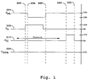
- Fig. 1 is a timing diagram showing voltage and timing control to bias the charge coupled device of Fig. 2.
- Fig. 1 plots voltage vs. time for the electrical potentials (i.e. control voltages) V PG 201, ⁇ X 202, ⁇ IC 210, and V SINK 220.
- the photogate region is biased electrically by controlling the amplitude of the photogate control voltage V PG 201 during the time that charge is not being transferred out of the photogate region for readout.
- this non-transfer time is shown as the time before 230 and after 235.
- V PG would be set below the level at which bias charge is induced during the non-transfer time before 230 and after 235.
- Prior art has stayed away from increasing the photogate control voltage higher than the level at which bias charge is induced exactly because a bias charge causes an offset in the device output signal.
- CCD's however demonstrate nonuniformities and offsets at the output when not exposed to any radiation. This is called the dark signal which is different for every single sensor.
- V PG is set to a level which will induce enough bias charge to bias the CCD such that it operates in a linear portion of its characteristic.
- V PG is shown to be 10 volts during the low time 234 - 235. In practice, we have found various voltages in the range of 8.5 - 15 volts to work well, depending on the particular CCD device.
- the integration control voltage control ⁇ IC 210 is the voltage applied to the integration control gate 23.
- ⁇ IC is used to control the actual exposure time.
- ⁇ IC is set to a low voltage level, the sink region 21 is isolated, and photon-generated charge will accumulate in the photogate region.
- ⁇ IC 210 is set to a high level at time 250, the sink region 21 is no longer isolated from the photogate region.
- V SINK 220 is set to a high voltage such as the 17 volts shown in Fig. 1, during the transition as ⁇ IC 210 is set to a high level, the sink 21 will act as a source and inject charge into the photogate region 10.
- the actual amount of charge transfer is controlled by the voltage differences between V PG , V SINK and ⁇ IC .
- the electrical bias as described here, is temperature dependent.
- a system is best able to use an electrical bias if the temperature of the CCD is held stable. In high end scanning systems, the temperature of the CCD device is held stable and low to reduce output signal drift and dark noise.
- Thermal control insures that constant control voltage levels will produce a stable bias that will not change over time. Since the thermal control is already part of the system, the electrical bias has the additional benefit of being much less complex and less expensive to implement than an additional thermal control that would be necessary to control the temperature of an optical bias source.
- An electrical bias is far superior than the prior art optical bias in that there is greatly reduced noise.
- An electrical bias does not involve a statistical process, and has a noise level that is an order of magnitude less than that of an optical bias.
- V PG 201 is set to a value between 8.0 and 15.5 volts during the transfer time. The value can be different for each CCD. For the most accurate results, each scanning system can be calibrated for that specific device.
- the voltage V PG 201 set is generally higher than the voltage recommended by the device manufacturers for normal operation, but not higher than the maximum rating specified by the device manufacturer.
- the anti-blooming circuitry is not being used for anti-blooming, so the signal levels shown in Fig. 1 are acceptable without additional manipulation of V SINK 220,, ⁇ IC 210, or V PG 201. It should be clear to one skilled in the art that use of the anti-blooming circuitry would require additional manipulation of these signals.
Landscapes
- Engineering & Computer Science (AREA)
- Multimedia (AREA)
- Signal Processing (AREA)
- Solid State Image Pick-Up Elements (AREA)
- Transforming Light Signals Into Electric Signals (AREA)
Description
- The present invention relates to image sensing and scanning in general, and more particularly to control of a charge coupled device type of radiation sensor according to the preamble of
claim 1. - Charge coupled devices are radiation sensors that are used to translate information such as graphic images and text into electrical signals. A scanned subject matter is exposed to radiation, usually in the form of light. The light reflects off of, or passes through, the scanned subject matter, and each of many sensors on a charge coupled device (CCD) detects the resulting levels of illumination. Electronic signals produced by the sensors are related to the intensity of the total incident radiation reflected or passed through the scanned subject matter. The electronic signals are used in the transmission, storage, or modification of the scanned information. Examples of devices in which charge coupled devices are used are the HORIZON, the HORIZON PLUS, and the SELECTSCAN document and transparency scanners manufactured by the Agfa Division of Miles Inc.. The SELECTSCAN uses a charge coupled device that has anti-blooming circuitry. Anti-blooming circuitry is built into a CCD of the type that is commercially available as the LORAL CCD 191 and the Kodak KLI8003, among others. The operation of such a CCD is described in many U.S. patents including U.S. 5,055,667 to Sayag.
- A CCD contains an array of photosensors. Radiation in the form of light impinges on the photosensors of a CCD and charge is generated that is proportional to the light on each photosensor. The photon-generated electrons are transported via the photogate to the transfer gate, and via the transfer gate to the shift registers. The charge in the shift registers is shifted out and converted to an electrical output signal by a charge-to-voltage converter.
- A problem that is well known in the art faces users of charge coupled devices. At very low radiation levels, the analog output is non-linear with respect to the radiation input. There are many reasons for this behavior, among which is Vertical Charge Transfer Loss and depletion of the photosensitive area. In high-precision applications, such non-linearity will complicate corrections made to compensate for non-uniformity of illumination of the array of sensors. This multiplicative type of correction, described in many patents including U.S. 4,748,515 to Van Daele and Pandelaers, is simple to implement if the charge coupled device behaves in a linear fashion. If the charge coupled device is non-linear, the correction can be very complex.
- One solution to avoiding non-linearity that is well known in the prior art is the addition of an optical bias. An optical bias is an additional radiation source which contributes to the total incident radiation in the system. Such a bias insures that the level of incident radiation will always be above the level at which the CCD is non-linear, insuring that the CCD operates in a sufficiently linear portion of its characteristic. An optical bias involves photo-conversion in that photons are converted to electrons. Photo-conversion is a statistical process featuring a Poisson distribution, so the root-mean-squared (RMS) noise associated with an optical bias is the square root of the freed electrons. An optical bias can contribute a significant amount of noise to the system noise.
- There are also thermal issues associated with keeping a constant optical bias level. In a CCD system, the maximum desired dark-level drift is 1/4 of the dark noise. Since the dynamic range can be described as the ratio of the dark noise to the saturation voltage, in a CCD system with a dynamic range of 1:15000 (dark noise normalized to 1) for example, the maximum allowable drift would be 1:60000. It is extremely difficult to operate a light emitting diode of the type that is usually used as an optical bias to within such a small drift without controlling the LED temperature. Temperature control of an LED adds complexity and expense to the system.
- US-A-5,055,667 on which the preamble of
claim 1 is based, describes a method of controlling the dynamic range of a CCD or a similar device. In this method a potential is applied to the control gate which is a magnitude causing all charge above a certain charge clipping level in the photogate region to pass the sink region and the magnitude of the potential is caused to vary during the exposure period according to a predetermined function. It however says nothing about how to avoid the non-linearity of the charge coupled devices at very low radiation levels. - It is an object of the present invention, therefore, to operate a charge coupled device in such a way as to avoid image artifacts such as streaking that would be apparent if a multiplicative correction algorithm was applied to a non-linear device.
- This object is solved by a method having the features of
claim 1. - The present invention allows to operate a charge coupled device in such a way as to avoid the need for complicated correction algorithms for illumination non-uniformity that would be otherwise necessary to avoid image artifacts.
- Further, the present invention allows to operate a charge coupled device to avoid both image artifacts and the need for complicated correction algorithms without adding noise, complexity, or cost to the system.
- A charge coupled device is voltage controlled so as to induce a small amount of bias charge in the photogate region. This charge serves to bias the device so that it operates in a linear fashion, especially when exposed to low radiation levels. Since the bias is produced electrically rather than optically, the noise level of the charge coupled device is reduced. The low radiation levels are offset to higher light levels which are in a more linear portion of the radiation response characteristic of the charge coupled device.
- The objects and features of the invention will best be understood from a detailed description of a preferred embodiment thereof selected for the purposes of illustration and shown in the accompanying drawings.
- Fig. 1
- is a timing diagram showing voltage and timing control to bias the charge coupled device of Fig. 2; and
- Fig. 2
- is a schematic depicting a prior art charge coupled device.
- Fig. 2 is a schematic depicting a prior art charge coupled device (CCD). The structure of the CCD includes anti-blooming architecture. The device contains a
photogate region 10 in which a photon generated charge accumulates. The charge is generated in thephotogate region 10 by radiant energy impinging upon the photosite 11 limited bylight shields 12. A photogate electrode 13 overlies thephotogate region 10. An electrical potential VPG is applied to photogate electrode 13, which maintains an electric field in thephotogate region 10 that causes charge to accumulate in the region. Thetransport gate region 16 is adjacent to the photogateregion 10. Charge packets accumulated in thephotogate region 10 are repeatedly transferred to thetransport gate region 16. Thetransport gate region 16 typically forms a part of a shift register or other transport structure for transporting the charge packet received from the photogate region to other circuit structures for processing. Overlyingtransport gate region 16 istransport gate electrode 17, to which an electrical potential ΦT is applied for enabling the accumulation of charge in thetransport gate 16. A transfer gate electrode 18 is disposed between photogateregion 10 andtransport gate 16. The passage of a charge packet from photogateregion 10 totransport gate 16 is determined by the electrical potential ΦX applied to transfer gate electrode 18. - Adjacent to photogate
region 10, on an opposite side from thetransport gate 16 is the anti-blooming architecture, including the sink region 21. Sink region 21 is attached to anelectrode 22 to which an electrical potential VSINK is applied to define the potential well for receiving excess charge. Anintegration control gate 23 is between photogateregion 10 and sink region 21. In anti-blooming operation, the electrical potential applied to theintegration control gate 23, ΦIC is used to control flow of excess charge to the sink. - In the present invention, the sink 21 is used as the source for a bias charge to bias the
photogate 10. The sink 21 is controlled to act both as an electron source and as a sink. Theintegration control 23 that in anti-blooming operation is used to control flow of excess charge from thephotogate 10 to the sink 21 also is used to control the flow of charge from the sink 21 to thephotogate 10. - Fig. 1 is a timing diagram showing voltage and timing control to bias the charge coupled device of Fig. 2. Fig. 1 plots voltage vs. time for the electrical potentials (i.e. control voltages)
V PG 201,Φ X 202,Φ IC 210, andV SINK 220. - The photogate region is biased electrically by controlling the amplitude of the photogate
control voltage V PG 201 during the time that charge is not being transferred out of the photogate region for readout. In Fig. 1 this non-transfer time is shown as the time before 230 and after 235. In prior art operation VPG would be set below the level at which bias charge is induced during the non-transfer time before 230 and after 235. Prior art has stayed away from increasing the photogate control voltage higher than the level at which bias charge is induced exactly because a bias charge causes an offset in the device output signal. CCD's however demonstrate nonuniformities and offsets at the output when not exposed to any radiation. This is called the dark signal which is different for every single sensor. In professional CCD applications, it is common to correct for all dark signal uniformities and offsets so inducing an extra offset as a consequence of biasing does not cause any extra effort. In the present invention, a small amount of bias charge is used to avoid non-linear CCD response, especially at low radiation levels. The voltage control VPG is set to a level which will induce enough bias charge to bias the CCD such that it operates in a linear portion of its characteristic. In Fig. 1, VPG is shown to be 10 volts during the low time 234 - 235. In practice, we have found various voltages in the range of 8.5 - 15 volts to work well, depending on the particular CCD device. - The integration control
voltage control Φ IC 210 is the voltage applied to theintegration control gate 23. ΦIC is used to control the actual exposure time. When ΦIC is set to a low voltage level, the sink region 21 is isolated, and photon-generated charge will accumulate in the photogate region. WhenΦ IC 210 is set to a high level attime 250, the sink region 21 is no longer isolated from the photogate region. IfV SINK 220 is set to a high voltage such as the 17 volts shown in Fig. 1, during the transition asΦ IC 210 is set to a high level, the sink 21 will act as a source and inject charge into thephotogate region 10. The actual amount of charge transfer is controlled by the voltage differences between VPG, VSINK and ΦIC. - In a very short time (sub-nanoseconds) after the charge transfer from the sink 21 to the
photogate region 10 begins, an electrical equilibrium is reached between the sink region 21 and thephotogate region 10 thereby establishing a bias charge in the photogate region. In the time after the equilibrium is established (250), and before the time ΦIC is lowered (255), any charge generated in the photogate region by photo-conversion disturbs the equilibrium, and the excess charge moves from thephotogate region 10 to the sink region. When ΦIC is lowered attime 255, the equilibrium charge remains in the photogate region. Therefore integration can start since the sink region is again isolated from the photogate region. - The prior art has taught away from the present invention because the electrical bias, as described here, is temperature dependent. A system is best able to use an electrical bias if the temperature of the CCD is held stable. In high end scanning systems, the temperature of the CCD device is held stable and low to reduce output signal drift and dark noise. Thermal control insures that constant control voltage levels will produce a stable bias that will not change over time. Since the thermal control is already part of the system, the electrical bias has the additional benefit of being much less complex and less expensive to implement than an additional thermal control that would be necessary to control the temperature of an optical bias source.
- An electrical bias is far superior than the prior art optical bias in that there is greatly reduced noise. An electrical bias does not involve a statistical process, and has a noise level that is an order of magnitude less than that of an optical bias.
- We have found that approximately 1% of the saturation charge level as an electrical bias will operate the LORAL CCD 191 in a sufficiently linear portion of its characteristic. In the present implementation of the invention,
V PG 201 is set to a value between 8.0 and 15.5 volts during the transfer time. The value can be different for each CCD. For the most accurate results, each scanning system can be calibrated for that specific device. Thevoltage V PG 201 set is generally higher than the voltage recommended by the device manufacturers for normal operation, but not higher than the maximum rating specified by the device manufacturer. - In the embodiment shown in Fig. 1, the anti-blooming circuitry is not being used for anti-blooming, so the signal levels shown in Fig. 1 are acceptable without additional manipulation of
V SINK 220,,Φ IC 210, orV PG 201. It should be clear to one skilled in the art that use of the anti-blooming circuitry would require additional manipulation of these signals.
Claims (3)
- A method of operating a charge coupled device having a radiation responsive photogate region (10), in which a photon generated charge accumulates and is read out, a photogate electrode (13) overlying the photogate region (10), said photogate electrode having an electrical potential of VPG (201) applied thereto, and a sink region (21) connected to the photogate region (10) by an integration control gate (23), said method comprising the step of applying an electrical potential VSINK (220) to the sink region (21) to define a potential well for receiving an excess charge from the photogate region (10),
characterized in that said method further comprises the step of, before accumulation of photon generated charge in the photogate region (10), applying an electrical potential ⊘IC (210) to the integration control gate (23) so that the sink region (21) is used as a potential source for establishing a bias charge in the radiation responsive photogate region (10) sufficient to cause the charge coupled device to operate in a generally linear portion of its radiation response characteristic. - The method according to claim 1 further comprising the steps of
during establishing of bias charge in the photogate region (10)a. setting VSINK(220) to a high voltage; andb. setting ⊘IC (210) to a potential level which is sufficiently high to allow a bias charge to transfer from the sink region (21) to the radiation responsive photogate region (10). - The method according to claim 2 further comprising the step of
during establishing of bias charge in the photogate region (10)
setting VPG (201) to a potential level which is high enough to attract a bias charge from the sink region (21) to the radiation responsive photogate (10).
Applications Claiming Priority (2)
| Application Number | Priority Date | Filing Date | Title |
|---|---|---|---|
| US24294094A | 1994-05-16 | 1994-05-16 | |
| US242940 | 1994-05-16 |
Publications (2)
| Publication Number | Publication Date |
|---|---|
| EP0683602A1 EP0683602A1 (en) | 1995-11-22 |
| EP0683602B1 true EP0683602B1 (en) | 2001-03-07 |
Family
ID=22916720
Family Applications (1)
| Application Number | Title | Priority Date | Filing Date |
|---|---|---|---|
| EP95104482A Expired - Lifetime EP0683602B1 (en) | 1994-05-16 | 1995-03-27 | Method and apparatus for a low noise, charge coupled device |
Country Status (3)
| Country | Link |
|---|---|
| EP (1) | EP0683602B1 (en) |
| JP (1) | JPH0851570A (en) |
| DE (1) | DE69520242T2 (en) |
Families Citing this family (2)
| Publication number | Priority date | Publication date | Assignee | Title |
|---|---|---|---|---|
| US6486503B1 (en) | 1994-01-28 | 2002-11-26 | California Institute Of Technology | Active pixel sensor array with electronic shuttering |
| EP0940029B1 (en) * | 1996-01-22 | 2004-06-23 | California Institute Of Technology | Active pixel sensor array with multiresolution readout |
Family Cites Families (7)
| Publication number | Priority date | Publication date | Assignee | Title |
|---|---|---|---|---|
| US3986198A (en) * | 1973-06-13 | 1976-10-12 | Rca Corporation | Introducing signal at low noise level to charge-coupled circuit |
| EP0033129B1 (en) * | 1980-01-25 | 1984-06-13 | Kabushiki Kaisha Toshiba | Charge transfer apparatus |
| EP0115225B1 (en) * | 1982-12-21 | 1987-05-06 | Thomson-Csf | Method for scanning a line-transfer photosensitive device, and apparatus for carrying out the method |
| US4620231A (en) * | 1984-06-18 | 1986-10-28 | Rca Corporation | CCD imager with photodetector bias introduced via the CCD register |
| DE3579922D1 (en) | 1985-10-07 | 1990-10-31 | Agfa Gevaert Nv | METHOD FOR CORRECTING A VIDEO OUTPUT SIGNAL. |
| US4912560A (en) * | 1988-01-29 | 1990-03-27 | Kabushiki Kaisha Toshiba | Solid state image sensing device |
| US5055667A (en) | 1990-06-21 | 1991-10-08 | Loral Fairchild Corporation | Non-linear photosite response in CCD imagers |
-
1995
- 1995-03-27 DE DE69520242T patent/DE69520242T2/en not_active Expired - Fee Related
- 1995-03-27 EP EP95104482A patent/EP0683602B1/en not_active Expired - Lifetime
- 1995-05-12 JP JP7114978A patent/JPH0851570A/en active Pending
Also Published As
| Publication number | Publication date |
|---|---|
| DE69520242D1 (en) | 2001-04-12 |
| DE69520242T2 (en) | 2001-09-06 |
| JPH0851570A (en) | 1996-02-20 |
| EP0683602A1 (en) | 1995-11-22 |
Similar Documents
| Publication | Publication Date | Title |
|---|---|---|
| US5204761A (en) | Pixel by pixel offset and gain correction in analog data from scanning arrays | |
| US7381936B2 (en) | Self-calibrating anti-blooming circuit for CMOS image sensor having a spillover protection performance in response to a spillover condition | |
| US3953733A (en) | Method of operating imagers | |
| KR100320310B1 (en) | Active type solid-state imaging device | |
| US4678938A (en) | Solid-state image sensing apparatus having an automatic control loop | |
| EP0511644B1 (en) | Solid-state image pickup device | |
| EP0773669B1 (en) | Circuit, pixel, device and method for reducing fixed pattern noise in solid state imaging devices | |
| US6921891B2 (en) | Photodetector with high dynamic range and increased operating temperature | |
| US6342920B2 (en) | Photoelectric conversion device | |
| US20120045146A1 (en) | Apparatus and method for eliminating artifacts in active pixel sensor (aps) imagers | |
| JPH08149376A (en) | Solid-state imaging device | |
| US6995797B2 (en) | Charge detecting device for a solid state imaging device | |
| US6917029B2 (en) | Four-component pixel structure leading to improved image quality | |
| KR100705005B1 (en) | Image pixel of CMOS image sensor | |
| US6445413B1 (en) | System for determining a video offset from dark photosensors in an image sensor array | |
| EP0683602A1 (en) | Method and apparatus for a low noise, charge coupled device | |
| US5642162A (en) | Charge transfer device having a signal processing circuit for correcting output voltage | |
| US7084911B1 (en) | Black level calibration method for imager with hysteresis comparison and adaptive step size | |
| US7327500B2 (en) | Image inputting apparatus | |
| US4562473A (en) | Dark current sensing with a solid-state imager having a CCD line register output | |
| US7236192B2 (en) | Image-sensing device | |
| US7576669B2 (en) | Method and apparatus for calibrating analog-to-digital converters within an imaging device | |
| US20030058358A1 (en) | Image pickup device with high contrast detection capability | |
| US20030098406A1 (en) | Solid-state image sensing device | |
| KR100255400B1 (en) | Ccd solid state image pickup device |
Legal Events
| Date | Code | Title | Description |
|---|---|---|---|
| PUAI | Public reference made under article 153(3) epc to a published international application that has entered the european phase |
Free format text: ORIGINAL CODE: 0009012 |
|
| AK | Designated contracting states |
Kind code of ref document: A1 Designated state(s): BE DE FR GB |
|
| 17P | Request for examination filed |
Effective date: 19960521 |
|
| RAP1 | Party data changed (applicant data changed or rights of an application transferred) |
Owner name: BAYER CORPORATION |
|
| 17Q | First examination report despatched |
Effective date: 19980417 |
|
| RAP1 | Party data changed (applicant data changed or rights of an application transferred) |
Owner name: AGFA CORPORATION |
|
| GRAG | Despatch of communication of intention to grant |
Free format text: ORIGINAL CODE: EPIDOS AGRA |
|
| GRAG | Despatch of communication of intention to grant |
Free format text: ORIGINAL CODE: EPIDOS AGRA |
|
| GRAH | Despatch of communication of intention to grant a patent |
Free format text: ORIGINAL CODE: EPIDOS IGRA |
|
| GRAH | Despatch of communication of intention to grant a patent |
Free format text: ORIGINAL CODE: EPIDOS IGRA |
|
| GRAA | (expected) grant |
Free format text: ORIGINAL CODE: 0009210 |
|
| AK | Designated contracting states |
Kind code of ref document: B1 Designated state(s): BE DE FR GB |
|
| PG25 | Lapsed in a contracting state [announced via postgrant information from national office to epo] |
Ref country code: BE Free format text: LAPSE BECAUSE OF FAILURE TO SUBMIT A TRANSLATION OF THE DESCRIPTION OR TO PAY THE FEE WITHIN THE PRESCRIBED TIME-LIMIT Effective date: 20010307 |
|
| REF | Corresponds to: |
Ref document number: 69520242 Country of ref document: DE Date of ref document: 20010412 |
|
| ET | Fr: translation filed | ||
| REG | Reference to a national code |
Ref country code: GB Ref legal event code: IF02 |
|
| PLBE | No opposition filed within time limit |
Free format text: ORIGINAL CODE: 0009261 |
|
| STAA | Information on the status of an ep patent application or granted ep patent |
Free format text: STATUS: NO OPPOSITION FILED WITHIN TIME LIMIT |
|
| 26N | No opposition filed | ||
| PGFP | Annual fee paid to national office [announced via postgrant information from national office to epo] |
Ref country code: FR Payment date: 20020227 Year of fee payment: 8 |
|
| PGFP | Annual fee paid to national office [announced via postgrant information from national office to epo] |
Ref country code: DE Payment date: 20020327 Year of fee payment: 8 |
|
| PGFP | Annual fee paid to national office [announced via postgrant information from national office to epo] |
Ref country code: GB Payment date: 20020328 Year of fee payment: 8 |
|
| PG25 | Lapsed in a contracting state [announced via postgrant information from national office to epo] |
Ref country code: GB Free format text: LAPSE BECAUSE OF NON-PAYMENT OF DUE FEES Effective date: 20030327 |
|
| PG25 | Lapsed in a contracting state [announced via postgrant information from national office to epo] |
Ref country code: DE Free format text: LAPSE BECAUSE OF NON-PAYMENT OF DUE FEES Effective date: 20031001 |
|
| GBPC | Gb: european patent ceased through non-payment of renewal fee |
Effective date: 20030327 |
|
| PG25 | Lapsed in a contracting state [announced via postgrant information from national office to epo] |
Ref country code: FR Free format text: LAPSE BECAUSE OF NON-PAYMENT OF DUE FEES Effective date: 20031127 |
|
| REG | Reference to a national code |
Ref country code: FR Ref legal event code: ST |