EP0681712B1 - Thin film electro-optical device with electrical connector - Google Patents
Thin film electro-optical device with electrical connector Download PDFInfo
- Publication number
- EP0681712B1 EP0681712B1 EP94904835A EP94904835A EP0681712B1 EP 0681712 B1 EP0681712 B1 EP 0681712B1 EP 94904835 A EP94904835 A EP 94904835A EP 94904835 A EP94904835 A EP 94904835A EP 0681712 B1 EP0681712 B1 EP 0681712B1
- Authority
- EP
- European Patent Office
- Prior art keywords
- electrode
- electrically conductive
- insulator
- connector
- electrically
- Prior art date
- Legal status (The legal status is an assumption and is not a legal conclusion. Google has not performed a legal analysis and makes no representation as to the accuracy of the status listed.)
- Expired - Lifetime
Links
- 239000010409 thin film Substances 0.000 title claims abstract description 49
- 239000000853 adhesive Substances 0.000 claims abstract description 55
- 230000001070 adhesive effect Effects 0.000 claims abstract description 55
- 239000012212 insulator Substances 0.000 claims abstract description 45
- 239000010408 film Substances 0.000 claims description 66
- 239000011159 matrix material Substances 0.000 claims description 28
- -1 poly(phenylene oxide) Polymers 0.000 claims description 27
- 239000002245 particle Substances 0.000 claims description 18
- 239000004983 Polymer Dispersed Liquid Crystal Substances 0.000 claims description 10
- 239000011521 glass Substances 0.000 claims description 8
- 229910052751 metal Inorganic materials 0.000 claims description 7
- 239000002184 metal Substances 0.000 claims description 7
- 229920001169 thermoplastic Polymers 0.000 claims description 7
- 230000008859 change Effects 0.000 claims description 6
- 230000005684 electric field Effects 0.000 claims description 6
- 230000003287 optical effect Effects 0.000 claims description 6
- 229920000728 polyester Polymers 0.000 claims description 5
- 229920001601 polyetherimide Polymers 0.000 claims description 5
- 239000004696 Poly ether ether ketone Substances 0.000 claims description 4
- 239000004697 Polyetherimide Substances 0.000 claims description 4
- 239000004642 Polyimide Substances 0.000 claims description 4
- 239000004820 Pressure-sensitive adhesive Substances 0.000 claims description 4
- 229920002492 poly(sulfone) Polymers 0.000 claims description 4
- 229920002530 polyetherether ketone Polymers 0.000 claims description 4
- 229920001721 polyimide Polymers 0.000 claims description 4
- 239000004416 thermosoftening plastic Substances 0.000 claims description 4
- 238000012546 transfer Methods 0.000 claims description 4
- 229920006380 polyphenylene oxide Polymers 0.000 claims description 3
- 229920001187 thermosetting polymer Polymers 0.000 claims description 3
- 239000004831 Hot glue Substances 0.000 claims description 2
- 230000004044 response Effects 0.000 claims description 2
- 230000037431 insertion Effects 0.000 abstract 1
- 238000003780 insertion Methods 0.000 abstract 1
- 239000000463 material Substances 0.000 description 32
- 239000004973 liquid crystal related substance Substances 0.000 description 22
- RYGMFSIKBFXOCR-UHFFFAOYSA-N Copper Chemical compound [Cu] RYGMFSIKBFXOCR-UHFFFAOYSA-N 0.000 description 20
- 238000010276 construction Methods 0.000 description 14
- 239000011889 copper foil Substances 0.000 description 14
- 239000011248 coating agent Substances 0.000 description 11
- 238000000576 coating method Methods 0.000 description 11
- 238000012360 testing method Methods 0.000 description 10
- 238000003475 lamination Methods 0.000 description 9
- 229920000642 polymer Polymers 0.000 description 8
- 229920002037 poly(vinyl butyral) polymer Polymers 0.000 description 6
- 229920000139 polyethylene terephthalate Polymers 0.000 description 6
- 239000005020 polyethylene terephthalate Substances 0.000 description 6
- BQCADISMDOOEFD-UHFFFAOYSA-N Silver Chemical compound [Ag] BQCADISMDOOEFD-UHFFFAOYSA-N 0.000 description 5
- 229910052802 copper Inorganic materials 0.000 description 5
- 239000010949 copper Substances 0.000 description 5
- 229910052709 silver Inorganic materials 0.000 description 5
- 239000004332 silver Substances 0.000 description 5
- 230000008901 benefit Effects 0.000 description 4
- 230000005540 biological transmission Effects 0.000 description 4
- 239000011888 foil Substances 0.000 description 4
- 238000000034 method Methods 0.000 description 4
- 238000012986 modification Methods 0.000 description 4
- 230000004048 modification Effects 0.000 description 4
- 229920006267 polyester film Polymers 0.000 description 4
- 239000003990 capacitor Substances 0.000 description 3
- 239000004020 conductor Substances 0.000 description 3
- 238000013461 design Methods 0.000 description 3
- 229920006254 polymer film Polymers 0.000 description 3
- PXHVJJICTQNCMI-UHFFFAOYSA-N Nickel Chemical compound [Ni] PXHVJJICTQNCMI-UHFFFAOYSA-N 0.000 description 2
- 229910052782 aluminium Inorganic materials 0.000 description 2
- XAGFODPZIPBFFR-UHFFFAOYSA-N aluminium Chemical compound [Al] XAGFODPZIPBFFR-UHFFFAOYSA-N 0.000 description 2
- 238000000149 argon plasma sintering Methods 0.000 description 2
- 239000000839 emulsion Substances 0.000 description 2
- 230000007613 environmental effect Effects 0.000 description 2
- PCHJSUWPFVWCPO-UHFFFAOYSA-N gold Chemical compound [Au] PCHJSUWPFVWCPO-UHFFFAOYSA-N 0.000 description 2
- 229910052737 gold Inorganic materials 0.000 description 2
- 239000010931 gold Substances 0.000 description 2
- AMGQUBHHOARCQH-UHFFFAOYSA-N indium;oxotin Chemical compound [In].[Sn]=O AMGQUBHHOARCQH-UHFFFAOYSA-N 0.000 description 2
- 238000010030 laminating Methods 0.000 description 2
- 229920001200 poly(ethylene-vinyl acetate) Polymers 0.000 description 2
- 229920003229 poly(methyl methacrylate) Polymers 0.000 description 2
- 239000004417 polycarbonate Substances 0.000 description 2
- 229920000515 polycarbonate Polymers 0.000 description 2
- 238000006116 polymerization reaction Methods 0.000 description 2
- 229920002635 polyurethane Polymers 0.000 description 2
- 239000004814 polyurethane Substances 0.000 description 2
- 238000011160 research Methods 0.000 description 2
- 230000002441 reversible effect Effects 0.000 description 2
- 230000003595 spectral effect Effects 0.000 description 2
- OXBLVCZKDOZZOJ-UHFFFAOYSA-N 2,3-Dihydrothiophene Chemical compound C1CC=CS1 OXBLVCZKDOZZOJ-UHFFFAOYSA-N 0.000 description 1
- NIXOWILDQLNWCW-UHFFFAOYSA-M Acrylate Chemical compound [O-]C(=O)C=C NIXOWILDQLNWCW-UHFFFAOYSA-M 0.000 description 1
- VYZAMTAEIAYCRO-UHFFFAOYSA-N Chromium Chemical compound [Cr] VYZAMTAEIAYCRO-UHFFFAOYSA-N 0.000 description 1
- 235000013175 Crataegus laevigata Nutrition 0.000 description 1
- 239000004988 Nematic liquid crystal Substances 0.000 description 1
- OAICVXFJPJFONN-UHFFFAOYSA-N Phosphorus Chemical compound [P] OAICVXFJPJFONN-UHFFFAOYSA-N 0.000 description 1
- RTAQQCXQSZGOHL-UHFFFAOYSA-N Titanium Chemical compound [Ti] RTAQQCXQSZGOHL-UHFFFAOYSA-N 0.000 description 1
- 239000005083 Zinc sulfide Substances 0.000 description 1
- PNEYBMLMFCGWSK-UHFFFAOYSA-N aluminium oxide Inorganic materials [O-2].[O-2].[O-2].[Al+3].[Al+3] PNEYBMLMFCGWSK-UHFFFAOYSA-N 0.000 description 1
- 238000013459 approach Methods 0.000 description 1
- 230000015572 biosynthetic process Effects 0.000 description 1
- 238000005266 casting Methods 0.000 description 1
- 230000015556 catabolic process Effects 0.000 description 1
- 238000006243 chemical reaction Methods 0.000 description 1
- 229910052593 corundum Inorganic materials 0.000 description 1
- 238000009826 distribution Methods 0.000 description 1
- 230000002708 enhancing effect Effects 0.000 description 1
- 230000008020 evaporation Effects 0.000 description 1
- 238000001704 evaporation Methods 0.000 description 1
- 229920005570 flexible polymer Polymers 0.000 description 1
- 238000010438 heat treatment Methods 0.000 description 1
- 239000012943 hotmelt Substances 0.000 description 1
- 238000010348 incorporation Methods 0.000 description 1
- 238000004519 manufacturing process Methods 0.000 description 1
- 230000007246 mechanism Effects 0.000 description 1
- 230000008018 melting Effects 0.000 description 1
- 238000002844 melting Methods 0.000 description 1
- 150000002739 metals Chemical class 0.000 description 1
- 238000002156 mixing Methods 0.000 description 1
- 239000000203 mixture Substances 0.000 description 1
- 229910052759 nickel Inorganic materials 0.000 description 1
- 230000005693 optoelectronics Effects 0.000 description 1
- 238000005191 phase separation Methods 0.000 description 1
- 239000004926 polymethyl methacrylate Substances 0.000 description 1
- 239000002243 precursor Substances 0.000 description 1
- 238000002360 preparation method Methods 0.000 description 1
- 230000008569 process Effects 0.000 description 1
- 230000005855 radiation Effects 0.000 description 1
- 230000009467 reduction Effects 0.000 description 1
- 238000009877 rendering Methods 0.000 description 1
- 238000005096 rolling process Methods 0.000 description 1
- 238000000926 separation method Methods 0.000 description 1
- 229920002379 silicone rubber Polymers 0.000 description 1
- 239000004945 silicone rubber Substances 0.000 description 1
- 229910001220 stainless steel Inorganic materials 0.000 description 1
- 239000010935 stainless steel Substances 0.000 description 1
- 238000007736 thin film deposition technique Methods 0.000 description 1
- 239000010936 titanium Substances 0.000 description 1
- 229910052719 titanium Inorganic materials 0.000 description 1
- 229910001845 yogo sapphire Inorganic materials 0.000 description 1
- 229910052984 zinc sulfide Inorganic materials 0.000 description 1
- DRDVZXDWVBGGMH-UHFFFAOYSA-N zinc;sulfide Chemical compound [S-2].[Zn+2] DRDVZXDWVBGGMH-UHFFFAOYSA-N 0.000 description 1
Images



Classifications
-
- H—ELECTRICITY
- H01—ELECTRIC ELEMENTS
- H01R—ELECTRICALLY-CONDUCTIVE CONNECTIONS; STRUCTURAL ASSOCIATIONS OF A PLURALITY OF MUTUALLY-INSULATED ELECTRICAL CONNECTING ELEMENTS; COUPLING DEVICES; CURRENT COLLECTORS
- H01R4/00—Electrically-conductive connections between two or more conductive members in direct contact, i.e. touching one another; Means for effecting or maintaining such contact; Electrically-conductive connections having two or more spaced connecting locations for conductors and using contact members penetrating insulation
- H01R4/04—Electrically-conductive connections between two or more conductive members in direct contact, i.e. touching one another; Means for effecting or maintaining such contact; Electrically-conductive connections having two or more spaced connecting locations for conductors and using contact members penetrating insulation using electrically conductive adhesives
-
- G—PHYSICS
- G02—OPTICS
- G02F—OPTICAL DEVICES OR ARRANGEMENTS FOR THE CONTROL OF LIGHT BY MODIFICATION OF THE OPTICAL PROPERTIES OF THE MEDIA OF THE ELEMENTS INVOLVED THEREIN; NON-LINEAR OPTICS; FREQUENCY-CHANGING OF LIGHT; OPTICAL LOGIC ELEMENTS; OPTICAL ANALOGUE/DIGITAL CONVERTERS
- G02F1/00—Devices or arrangements for the control of the intensity, colour, phase, polarisation or direction of light arriving from an independent light source, e.g. switching, gating or modulating; Non-linear optics
- G02F1/01—Devices or arrangements for the control of the intensity, colour, phase, polarisation or direction of light arriving from an independent light source, e.g. switching, gating or modulating; Non-linear optics for the control of the intensity, phase, polarisation or colour
- G02F1/13—Devices or arrangements for the control of the intensity, colour, phase, polarisation or direction of light arriving from an independent light source, e.g. switching, gating or modulating; Non-linear optics for the control of the intensity, phase, polarisation or colour based on liquid crystals, e.g. single liquid crystal display cells
- G02F1/133—Constructional arrangements; Operation of liquid crystal cells; Circuit arrangements
- G02F1/1333—Constructional arrangements; Manufacturing methods
- G02F1/1345—Conductors connecting electrodes to cell terminals
-
- B—PERFORMING OPERATIONS; TRANSPORTING
- B32—LAYERED PRODUCTS
- B32B—LAYERED PRODUCTS, i.e. PRODUCTS BUILT-UP OF STRATA OF FLAT OR NON-FLAT, e.g. CELLULAR OR HONEYCOMB, FORM
- B32B17/00—Layered products essentially comprising sheet glass, or glass, slag, or like fibres
- B32B17/06—Layered products essentially comprising sheet glass, or glass, slag, or like fibres comprising glass as the main or only constituent of a layer, next to another layer of a specific material
- B32B17/10—Layered products essentially comprising sheet glass, or glass, slag, or like fibres comprising glass as the main or only constituent of a layer, next to another layer of a specific material of synthetic resin
- B32B17/10005—Layered products essentially comprising sheet glass, or glass, slag, or like fibres comprising glass as the main or only constituent of a layer, next to another layer of a specific material of synthetic resin laminated safety glass or glazing
- B32B17/10009—Layered products essentially comprising sheet glass, or glass, slag, or like fibres comprising glass as the main or only constituent of a layer, next to another layer of a specific material of synthetic resin laminated safety glass or glazing characterized by the number, the constitution or treatment of glass sheets
- B32B17/10036—Layered products essentially comprising sheet glass, or glass, slag, or like fibres comprising glass as the main or only constituent of a layer, next to another layer of a specific material of synthetic resin laminated safety glass or glazing characterized by the number, the constitution or treatment of glass sheets comprising two outer glass sheets
-
- B—PERFORMING OPERATIONS; TRANSPORTING
- B32—LAYERED PRODUCTS
- B32B—LAYERED PRODUCTS, i.e. PRODUCTS BUILT-UP OF STRATA OF FLAT OR NON-FLAT, e.g. CELLULAR OR HONEYCOMB, FORM
- B32B17/00—Layered products essentially comprising sheet glass, or glass, slag, or like fibres
- B32B17/06—Layered products essentially comprising sheet glass, or glass, slag, or like fibres comprising glass as the main or only constituent of a layer, next to another layer of a specific material
- B32B17/10—Layered products essentially comprising sheet glass, or glass, slag, or like fibres comprising glass as the main or only constituent of a layer, next to another layer of a specific material of synthetic resin
- B32B17/10005—Layered products essentially comprising sheet glass, or glass, slag, or like fibres comprising glass as the main or only constituent of a layer, next to another layer of a specific material of synthetic resin laminated safety glass or glazing
- B32B17/10165—Functional features of the laminated safety glass or glazing
- B32B17/10431—Specific parts for the modulation of light incorporated into the laminated safety glass or glazing
- B32B17/10467—Variable transmission
- B32B17/10495—Variable transmission optoelectronic, i.e. optical valve
- B32B17/10504—Liquid crystal layer
-
- B—PERFORMING OPERATIONS; TRANSPORTING
- B32—LAYERED PRODUCTS
- B32B—LAYERED PRODUCTS, i.e. PRODUCTS BUILT-UP OF STRATA OF FLAT OR NON-FLAT, e.g. CELLULAR OR HONEYCOMB, FORM
- B32B17/00—Layered products essentially comprising sheet glass, or glass, slag, or like fibres
- B32B17/06—Layered products essentially comprising sheet glass, or glass, slag, or like fibres comprising glass as the main or only constituent of a layer, next to another layer of a specific material
- B32B17/10—Layered products essentially comprising sheet glass, or glass, slag, or like fibres comprising glass as the main or only constituent of a layer, next to another layer of a specific material of synthetic resin
- B32B17/10005—Layered products essentially comprising sheet glass, or glass, slag, or like fibres comprising glass as the main or only constituent of a layer, next to another layer of a specific material of synthetic resin laminated safety glass or glazing
- B32B17/1055—Layered products essentially comprising sheet glass, or glass, slag, or like fibres comprising glass as the main or only constituent of a layer, next to another layer of a specific material of synthetic resin laminated safety glass or glazing characterized by the resin layer, i.e. interlayer
- B32B17/10761—Layered products essentially comprising sheet glass, or glass, slag, or like fibres comprising glass as the main or only constituent of a layer, next to another layer of a specific material of synthetic resin laminated safety glass or glazing characterized by the resin layer, i.e. interlayer containing vinyl acetal
-
- H—ELECTRICITY
- H05—ELECTRIC TECHNIQUES NOT OTHERWISE PROVIDED FOR
- H05B—ELECTRIC HEATING; ELECTRIC LIGHT SOURCES NOT OTHERWISE PROVIDED FOR; CIRCUIT ARRANGEMENTS FOR ELECTRIC LIGHT SOURCES, IN GENERAL
- H05B33/00—Electroluminescent light sources
- H05B33/02—Details
- H05B33/06—Electrode terminals
Definitions
- Mori describes an electroluminescent device having an "auxiliary electrode” in the form of a long narrow strip.
- the purpose of the "auxiliary electrode” is to distribute voltage over the entire electroluminescent layer and to provide a connection to the power supply. It consists of a conductive metal layer sandwiched between an insulating layer and an electrically conductive adhesive.
- the "auxiliary electrode,” in turn, is sandwiched between the electroluminescent layer and the electrode of the device such that the insulating layer contacts one face of the electroluminescent layer, while the adhesive contacts one face of the electrode.
- the "auxiliary electrode” is not inserted into the electroluminescent layer.
- the invention provides a reliable electrical connection between the electrode of a thin film device and an external power supply.
- the compact design of the electrical connector (which is placed along only a single edge of the device) facilitates use of thin film devices incorporating the connector in applications such as architectural and automotive panels and windows.
- the connector enables the panel or window to be trimmed to size along its total perimeter except for the relatively small area where the connector is positioned. It also enables the device to be used with a variety of geometrically shaped panels and windows.
- prior art connectors which typically require connections along the length of two opposed edges of the device, could only be used with difficulty in panels and windows having geometries other than square or rectangular.
- the connector is incorporated into the thin film device as part of the lamination procedure, the devices may be readily manufactured in a cost-effective assembly.
- Fig. 1 is a perspective view of a thin film device having an electrical connector according to one embodiment of the invention.
- Fig. 5 is a perspective view of a thin film device having an electrical connector according to a third embodiment of the invention.
- the polymer film also forms a seal around the electrodes and electrically responsive layer following lamination to enhance environmental resistance.
- Suitable materials for the film include poly(vinyl butyral), polyurethanes that flow at the temperatures used for lamination, and ethylene vinyl acetate copolymers, with poly(vinyl butyral) being preferred.
- Suitable materials for the film include copper, silver, aluminum, gold, and other high conductivity metals.
- the film preferably is metallized to the face of the insulator (in which case the film thickness is closer to 0.1 ⁇ m) or adhered to the face using an adhesive; in the latter case, the film is preferably provided in the form of a foil (e.g., a copper foil), in which case the thickness can approach to 100 ⁇ m.
- a connector element having a typical construction comprising a central, 25 ⁇ m thick polyester insulating film, approximately 3cm in width and 10.2cm in length, having a strip of 0.6cm wide copper foil tape (# 1181, available from 3M, St. Paul, MN) adhered to the opposing faces of the insulating film in a staggered configuration such that there was a separation of at least about 1mm between the projection of one strip onto the opposing face of the insulator film and the copper strip on that face of the film.
- a connector element having a typical construction comprising a central, 25 ⁇ m thick polyester insulating film, approximately 3cm in width and 10.2cm in length, having a strip of 0.6cm wide copper foil tape (# 1181, available from 3M, St. Paul, MN) adhered to the opposing faces of the insulating film in a staggered configuration such that there was a separation of at least about 1mm between the projection of one strip onto the opposing face of the insulator film and the copper
- Thin film light modulating devices were prepared by carefully rolling the liquid crystal matrix-free edges of the electrode films back, placing the connector element between the electrode films such that the central insulating strip extended into the cured liquid crystal matrix approximately 3mm, applying a conductive adhesive to the copper foil tape, repositioning the electrode films over the connector element and laminating the device with heat (typically 65-75°C) and pressure (typically 1.5 x 10 5 Pa) for a period of approximately 10-20 sec. All areas of the electrode film that were not separated by the connector element or the cured PDLC matrix were trimmed to prevent electrical shorting of the device.
- the electrode and electrically responsive layer assembly may be displaced relative to both opposed edges of the device.
Landscapes
- Physics & Mathematics (AREA)
- Nonlinear Science (AREA)
- Chemical & Material Sciences (AREA)
- Crystallography & Structural Chemistry (AREA)
- Optics & Photonics (AREA)
- General Physics & Mathematics (AREA)
- Mathematical Physics (AREA)
- Connections Effected By Soldering, Adhesion, Or Permanent Deformation (AREA)
- Liquid Crystal (AREA)
- Coupling Device And Connection With Printed Circuit (AREA)
- Push-Button Switches (AREA)
- Electrochromic Elements, Electrophoresis, Or Variable Reflection Or Absorption Elements (AREA)
- Electroluminescent Light Sources (AREA)
Abstract
Description
- This invention relates to electrical connectors in thin film devices (i.e., devices having one or more thin film electrodes in which the thickness of each electrode is less than about, e.g., 2µm) having an electrically responsive layer designed to deliver electric current from a power supply to an electrode.
- Many types of thin film devices having an electrically responsive layer are known. They include thin film electro-optical devices in which the optical properties of the electrically responsive layer change. Electric current is supplied to the device by means of a connector that delivers current from an external power supply to at least one electrode in contact with the electrically responsive layer.
- One example of a thin film electro-optical device is an electrochromic device. Such a device relies upon a reversible chemical reaction that takes place in the electrically responsive layer upon application of current to cause a change in optical properties.
- A second example is a display device containing a layer of electrically responsive liquid crystal material. Application of an electric field causes the alignment, and thus the optical properties, of the liquid crystal layer to change.
- A third example is the so-called Nematic Curvilinear Aligned Phase ("NCAP") device described, e.g., in Fergason, U.S. Patent No. 4,435,047. These devices include an electrically responsive liquid crystal layer in which nematic liquid crystal material is encapsulated in a polymer matrix. The encapsulated material is prepared by combining the liquid crystal material with the polymer matrix in the form of an aqueous emulsion, and then casting a film from the emulsion. These devices are relatively translucent in the absence of an electric field due to light scattering, but are relatively transparent upon application of a field.
- A fourth example of electro-optical device is the Polymer-Dispersed Liquid Crystal ("PDLC") device described, e.g., in Doane et al., U.S. 4,688,900. These devices include an electrically responsive liquid crystal layer in which liquid crystal droplets are dispersed throughout a polymer matrix. The liquid crystal layer is prepared by combining the liquid crystal material with a polymerizable matrix precursor and then subjecting the mixture to polymerization conditions. Polymerization causes phase separation of the liquid crystal material, resulting in the formation of liquid crystal droplets dispersed throughout the polymerized matrix. Like the NCAP devices, these PDLC devices are translucent in the absence of an electric field due to light scattering and become transparent upon application of the field.
- Reverse mode PDLC devices are also known. These devices are transparent in the absence of an electric field and become translucent upon application of the field.
- A fifth example is an electroluminescent device. In such a device, the electrically responsive layer consists of electrically responsive particles (e.g., zinc sulfide) that luminesce upon application of current.
- In all of these devices, it is necessary to establish an electrical connection between the electrode and the power supply. One example of such a connector is shown in Mori et al., U.S. 4,956,031. Mori describes an electroluminescent device having an "auxiliary electrode" in the form of a long narrow strip. The purpose of the "auxiliary electrode" is to distribute voltage over the entire electroluminescent layer and to provide a connection to the power supply. It consists of a conductive metal layer sandwiched between an insulating layer and an electrically conductive adhesive. The "auxiliary electrode," in turn, is sandwiched between the electroluminescent layer and the electrode of the device such that the insulating layer contacts one face of the electroluminescent layer, while the adhesive contacts one face of the electrode. The "auxiliary electrode" is not inserted into the electroluminescent layer.
- The connection between the power supply and electrode is often the source of failure in thin film devices, resulting in melting and subsequent arcing of the electrode layer. There is a need, therefore, for a compact electrical connector that provides a reliable connection between the power supply and electrode of such thin film devices.
- DE-A-3 638 858 discloses a thin film electro-optical device as specified in the preambles of
claims - The invention is related to a thin film electro-optical device as defined in
claims - More particularly, the device of the present invention comprises an electrical connector placed along a single edge of a thin film device having an electrically responsive layer,
- said connector being configured to deliver electric current from a power supply to at least one electrode in electrical contact with the electrically responsive layer,
- said connector comprising
- a flexible insulator having on at least one face an electrically conductive portion adapted to establish electrical contact between an electrode of a thin film device and a power supply, at least a portion of said insulator being inserted into a portion of the electrically responsive layer of the device, and
- connector means in electrical contact with the electrically conductive portion of said insulator and adapted to establish electrical contact with a power supply.
-
- The inventive device further comprises an electrically conductive adhesive provided on the electrically conductive portion of the insulator adapted to be placed adjacent to the electrode to establish electrical contact with the electrode. The electrically conductive adhesive includes electrically conductive particles dispersed throughout an adhesive matrix in which the effective contact area between the electrically conductive particles and the electrode of the device (i.e., the portion of the adhesive which is actually electrically conductive) is sufficiently high to ensure current transfer while minimizing heat build-up in the area of the electrode directly beneath the conductive particles.
- In most preferred embodiments, the electrically conductive adhesive is flexible. Examples of suitable adhesives include pressure sensitive adhesives, hot melt adhesives, thermoset adhesives, and thermoplastic adhesives. The thickness of the adhesive on each electrically conductive portion preferably is no greater than about 50µm.
- Examples of suitable materials for the insulator include films such as polyester (e.g., poly(ethylene terephthalate) or poly(ethylene naphthalate)), polyimide, polyether imide, polysulfone, poly(phenylene oxide), and polyether ether ketone films. Other suitable materials for the insulator include non-electrically conductive adhesives. One or both faces of the insulator may be provided with an electrically conductive portion; in the latter case (which is useful for establishing electrical connections to multiple electrode areas), both electrically conductive portions are provided with an electrically conductive adhesive.
- The electrically conductive portion of the insulator preferably includes at least one metal strip in contact with at least a portion of a face of the insulator. Contact may be established by adhering or metallizing the strip to the insulator face; the strip may also simply be placed against the insulator face. Preferred materials for the electrically conductive portion include silver and copper.
- In one embodiment, for example, the insulator is a poly(ethylene terephthalate) film and each electrically conductive portion includes a copper foil adhered to at least a portion of a face of the film. In another embodiment, the insulator is also a poly(ethylene terephthalate) film, but each electrically conductive portion includes a silver strip metallized to at least a portion of a face of the film.
- The connector means may include at least one wire connector pad. This pad may be soldered, adhered, or otherwise attached to the electrically conductive portions of the insulator. Alternatively, the electrically conductive portion itself may form the connector means if its thickness is sufficient to provide a mechanically stable and electrically conductive connection.
- The invention features a thin film electro-optical device (e.g., an electro-optical device in which the optical properties of the electrically responsive layer change upon application of electric current) incorporating the above-described electrical connector. Examples of suitable devices include electro-optical devices in which the electrically responsive layer is an electroluminescent layer, an electrochromic layer, a liquid crystal layer, a PDLC layer, or an NCAP layer.
- The electrode of the device (which extends beyond the electrically responsive layer) may be provided with a buss bar to distribute current throughout the electrode. The device may also further include a power supply, e.g., a line-operated zero cross power supply.
- The electrically responsive layer and the electrode of the device preferably are sandwiched between two sheets of optically clear glazing material (e.g., glass or a polymer such as polycarbonate or poly(methyl methacrylate)), and the electrical connector is configured such that the connector means and a portion of the insulator (and its associated electrically conductive portion) lie beyond the edge of at least one of the sheets such that electrical contact with a power supply is established beyond the edge of at least one of the sheets. The inner surfaces of the optically clear glazing material may further be provided with a layer of an optically clear thermoplastic polymer that flows at the temperatures used to laminate the components of the device together. Examples of suitable polymers include poly(vinyl butyral), polyurethanes displaying thermoplastic properties in the range of lamination temperatures, and ethylene vinyl acetate copolymers.
- In one embodiment of the above-described device, the sheets may be offset relative to each other, in which case the connector means and a portion of the insulator (and its associated electrically conductive portion) lie beyond the edge of only one of the sheets such that electrical contact with the power supply is established beyond the edge of only one of the sheets. In another embodiment, the sheets are aligned with each other such that the connector means and a portion of the insulator (and its associated electrically conductive portion) lie beyond the edges of both sheets, in which case electrical contact with the power supply is established beyond the edge of both sheets as well.
- The invention provides a reliable electrical connection between the electrode of a thin film device and an external power supply. In addition, the compact design of the electrical connector (which is placed along only a single edge of the device) facilitates use of thin film devices incorporating the connector in applications such as architectural and automotive panels and windows. The connector enables the panel or window to be trimmed to size along its total perimeter except for the relatively small area where the connector is positioned. It also enables the device to be used with a variety of geometrically shaped panels and windows. In contrast, prior art connectors, which typically require connections along the length of two opposed edges of the device, could only be used with difficulty in panels and windows having geometries other than square or rectangular. Moreover, because the connector is incorporated into the thin film device as part of the lamination procedure, the devices may be readily manufactured in a cost-effective assembly.
- Other features and advantages will be apparent from the following description of the preferred embodiments, and from the claims.
- Fig. 1 is a perspective view of a thin film device having an electrical connector according to one embodiment of the invention.
- Fig. 2 is a cross-sectional view, taken at 2-2, of the structure shown in Fig. 1 expanded to show detail.
- Fig. 3 is a perspective view of a thin film device having an electrical connector according to a second embodiment of the invention.
- Fig. 4 is a cross-sectional view, taken at 4-4, of the structure shown in Fig. 3 expanded to show detail.
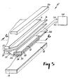
- Fig. 5 is a perspective view of a thin film device having an electrical connector according to a third embodiment of the invention.
- Fig. 6 is a cross-sectional view, taken at 6-6, of the structure shown in Fig. 5 expanded to show detail.
- Referring to Figs. 1 and 2, there is shown an electro-
optical device 10 featuring an electricallyresponsive layer 24 sandwiched between a pair ofelectrodes responsive layer 24 such that there is a gap between the two electrodes. Electricallyresponsive layer 24 may be, e.g., an electroluminescent, electrochromic, liquid crystal, PDLC, or NCAP layer. Suitable materials for the conductive portion ofelectrodes -
Electrodes responsive layer 24, in turn, are sandwiched between a pair of opticallyclear sheets 12, 14 (thickness of each sheet equals approximately 0.3 cm). Suitable materials for the sheet include glass and optically clear polymers such as polycarbonate and poly(methyl methacrylate). The inner surface of each sheet in contact with the electrodes is provided with afilm 16, 18 (each approximately 375µm thick) of a thermoplastic polymer that flows at the lamination temperatures and pressures used to assemble the device. The purpose of the polymer film is two-fold. First, it bonds the electrically responsive layer to opticallyclear sheets sheets - In the embodiment shown in Figs. 1 and 2,
sheets electrodes - An insulator film 26 (thickness approximately 25-100µm) inserted partially into electrically responsive layer and extending beyond the outer edges of
electrodes insulator 26 include polyesters such as poly(ethylene terephthalate) and poly(ethylene naphthalate), polyimides, polyether imides, polysulfones, poly(phenylene oxides), and polyether ether ketone, with poly(ethylene terephthalate) being preferred. Each face ofinsulator 26 is provided with an electricallyconductive film - The portion of
insulator 26 lying betweenelectrodes conductive films - The effective contact area between the electrically conductive particles and the electrode of the device is chosen such that it is sufficiently high to ensure current transfer while minimizing heat build-up in the area of the electrode directly beneath the conductive particles. In this way, electrode breakdown and subsequent arcing is minimized, while at the same time minimizing connector size. The effective contact area for a particular device is chosen based upon factors such as the surface area of the electrodes, the thickness of the adhesive, the thickness of the electrodes, the ability to conduct heat away from the connector area, and the material used to form the electrode (e.g., the conductivity and thermal stability of that material), all of which influence effective contact area. It is within the ability of a person of ordinary skill in the art to select appropriate contact areas based upon these parameters.
- The portion of
insulator 26 extending beyond the outer edge ofelectrodes electrodes 20, 22) andpower supply 54. A pair of insulatingpads 36, 38 (0.16 cm X 0.95 cm), each of which is provided with a copper foil busswire connector pad 40, 42 (thickness approximately 25µm each) connects a pair of wire leads 50, 52 frompower supply 54 todevice 10; the leads are soldered to copper foil busses 40, 42. An adhesive 44, 46 (thickness approximately 12.5µm) placed between the copper busses and the electrically conductive films establishes the electrical connection to the electrically conductive films (and thus electrically responsive layer 24). A variety of electrically conductive adhesives are suitable for adhesive 44, 46. Examples include the Creative Materials 108-10 and 3M 9703 adhesives described above. During lamination, thethermoplastic polymer films pad - A second embodiment is shown in Figs. 3 and 4. This embodiment is similar to the embodiment shown in Figs. 1 and 2, except that optically
clear sheets electrodes insulator 26 and associated conductingfilms wire connector pads pads adhesive portions 44, 46) rests. The advantage of this arrangement is that it obviates the need for a separate clip to hold the connector together, and enables production of a more compact device because the electrical connector does not protrude beyond the outer edge of the device (i.e., beyond the outer edges of bothsheets 12 and 14). - A third embodiment is shown in Figs. 5 and 6. Like the embodiment shown in Figs. 3 and 4,
sheets electrodes responsive layer 24 are displaced relative to one edge ofsheets polymer films cover 56 helps secure the connector elements tosheets films silicone rubber boot 58 preferably surrounds and protects the wire leads 50, 52; other suitable materials for the insulating film include polyester (e.g., poly(ethylene terephthalate) or poly(ethylene naphthalate)), polyimide, polyether imide, polysulfone, poly(phenylene oxide), and polyether ether ketone, together with a suitable non-electrically conductive adhesive. - Another difference between this embodiment and previous embodiments is that in this
embodiment device 10 lacks separate wire connector pads (such as copper foil busses 40, 42 shown in Figs. 1-4) to establish a connection to thewires power supply 54. Instead, electricallyconductive portions 28, 30 (e.g., in the form of copper foils) perform this role. The thickness ofportions portions wires portions wire connector pads - The invention will be further understood by reference to the following examples.
- Three different electrode films (i.e., polymer backing films to which a thin electrically conductive film had been applied) were evaluated in conjunction with the connector devices of the present invention. These materials were:
- Electrode
Film Type A A 50 micron thick polyester film with a vapor deposited Ag coating prepared by standard Ag coating or evaporation techniques, which was 15nm thick, having a resistivity of 4 ohms/square and a luminous transmission of about 50%, further comprising a thin, passivating Al2O3 coating, approximately 45nm thick, which was vapor deposited over the Ag coating using a process similar to that disclosed in Cox, J.T., Hass, G., and Ramsey, J.B., "Improved Dielectric Films for Multilayer Coating and Mirror Protection," J. de Phys. 25 (1964) pp. 250-54 to produce a film having a laminous transmission of about 60-70%; - Electrode
Film Type B A 50 micron thick polyester film with a 120nm thick vapor deposited indium tin oxide (ITO) coating having a resistivity of 70 ohms/square and a luminous transmission of 80%; and - Electrode
Film Type C A 50 micron thick polyester film with a 120nm thick vapor deposited ITO coating having a resistivity of 70 ohms/square and a luminous transmission of 80%, the electrode having an additional stripe of a thicker, substantially opaque Ag buss bar coating underneath the ITO coating approximately 70nm thick and having a resistivity of 0.67 ohms/square along one edge. The ITO coating was applied to the buss bar by standard thin film deposition techniques. -
- Active thin film light modulating PDLC matrices were prepared in a manner similar to the following procedure. Equal parts by weight of liquid crystal material BL036 (available from EM Industries, Hawthorne, New York) and Norland NOA65 (a thiol-ene based matrix material available from Norland Products, Inc., New Brunswick, NJ) were heated to approximately 60°C, with mixing, until the liquid crystal material completely dissolved. The resulting liquid crystal solution was poured between two electrode films which were held with their conductive faces in a facing relationship by the nip rollers of a precision coater. The gap between the nip rollers was set to provide an uncured liquid crystal matrix coating thickness of 15 to 21 microns. The unpolymerized liquid crystal matrix solution was introduced into the space between the two electrode films such that it left an uncoated strip approximately 3cm in width along one edge of the sandwich construction.
- The liquid crystal matrix solution was polymerized by positioning the sandwich construction comprising the two electrode films and the uncured liquid crystal matrix solution between, e.g., a pair of opposed banks of fluorescent phosphor lighting elements, each bank being positioned to illuminate one of the electrode films, to produce the active thin film light modulating matrix. Lighting elements having spectral distribution between 280 and 400nm are suitable for curing the matrix materials. For convenience, a lamp having a maximum output at 351nm was employed. The lighting elements were adjusted so as to provide an average intensity of 1.1 mW/cm2 through each electrode film. Each side of the sandwich construction received a total energy exposure of 100mJ/cm2. The construction as a whole was exposed to a total energy of 200mJ/cm2. The level of incident radiation was determined with an EIT low intensity UVIMAP radiometer having a spectral response in the range of 300 to 400nm with a maximum at 358nm.
- Current was delivered from a power supply to the active thin film modulating PDLC matrix through a connector element having a typical construction comprising a central, 25µm thick polyester insulating film, approximately 3cm in width and 10.2cm in length, having a strip of 0.6cm wide copper foil tape (# 1181, available from 3M, St. Paul, MN) adhered to the opposing faces of the insulating film in a staggered configuration such that there was a separation of at least about 1mm between the projection of one strip onto the opposing face of the insulator film and the copper strip on that face of the film. The copper strips were offset from the edge of the insulating film by at least 3mm and copper wire leads were soldered to one end of each copper foil tape strip to provide an electrical connection to a power supply. Electrical connection between the connector element and the electrodes of the conductor film was achieved by means of a conductive adhesive which was placed between the copper foil strip and the liquid crystal matrix-free portions of the electrode films.
- Thin film light modulating devices were prepared by carefully rolling the liquid crystal matrix-free edges of the electrode films back, placing the connector element between the electrode films such that the central insulating strip extended into the cured liquid crystal matrix approximately 3mm, applying a conductive adhesive to the copper foil tape, repositioning the electrode films over the connector element and laminating the device with heat (typically 65-75°C) and pressure (typically 1.5 x 10⁵ Pa) for a period of approximately 10-20 sec. All areas of the electrode film that were not separated by the connector element or the cured PDLC matrix were trimmed to prevent electrical shorting of the device.
- Examples 1 - 3 examined the role that the electrode film plays in the service life of the active thin film light modulating device. In these Examples, all of the active thin film light modulating devices were connected to a Staco Variac power supply (available from Staco Inc., Dayton, OH) which delivered a 120 volt switch current, the pad area was 6.4 cm2, the window area/connector area ratio was maintained at 154, an approximately 0.05mm thick layer of a conductive pressure sensitive adhesive (an acrylate-based pressure sensitive adhesive having an approximately 5% by weight loading of 20-40 micron sized silver-coated nickel particles, # 9703, available from 3M, St. Paul, MN) was utilized as the connective adhesive between the copper foil strip and the electrode film, and the test current was 0.03 amps.
- The computer-controlled switching test consisted of applying power for 2 seconds, followed by 2 seconds off, while current, voltage, and a.c. power were measured with a Valhalla 2301 power meter (Valhalla Scientific, San Diego, CA). The test ended if the current sharply declined, indicating failure.
- Switching service life data for various electrode film configurations are reported in Table 1.
Electrode Film/Switch Life Data Example Electrode Film Type # Switches before failure 1 Type A 1 2 Type B 15,000 31 Type C 15,000 - The data in Table 1 suggest that the ITO based electrode films, with or without a thick Ag buss bar, are preferred as they provide superior switching service life.
- The impact of the conductive adhesive on the switching service life of active thin film light modulating devices was studied utilizing the device construction of Example 2, except that a 1.3cm wide copper foil tape was used, the pad area was 12.9cm2, the window area/connector area ratio was maintained at 540, a line-operated zero cross power switch was substituted for the Variac, various conductive adhesives were utilized to achieve electrical connection between the copper foil tape and the electrode film, and the test current was 0.23 amps. The device construction of Example 2 was selected for this study as it subjects the electrical connection interface between the connector element and the electrode film to very demanding conditions.
- The thin film device was powered directly from a 120 volt, A.C., 60 Hz power line using a line-operated zero cross switch rated to switch at 3 volts or less (typically 1.8 volts) that displayed a maximum voltage spike of less than about 6 volts. The switch was based in part on a design generally described in Gemp, H., "Applications of Zero Voltage Crossing Optically Isolated Triac Devices," Motorola Optoelectronic Device Data (1988), pp. 9-72, except for modifications which provided for (a) powering the zero cross control circuitry within the device directly from the line (hence the term "line-operated"), rather than using an independent power source, and (b) the incorporation of input and output filters into the circuit. Both modifications were incorporated into the design to minimize the occurrence of switching-induced voltage spikes being fed to the thin film device.
- With respect to the first modification, line-operated power for the zero cross power control circuitry was obtained in space efficient manner using a voltage drop module comprising a capacitor connected in parallel to a current safety bleed resistor. The voltage drop module operated in conjunction with a rectifier module and a filter module comprising a voltage rectifier and capacitor. With respect to the second modification, the input and output filters each comprised a 0.47 µF, 400 volt capacitor, with the input filter incorporated between the power source and the input leads of the thin film device, and the output filter interposed between the zero cross switch output leads and the thin film device.
- A further reduction in the occurrence of switching-induced voltage spikes was realized by keeping the power circuit to the thin film device on at all times and energizing the device by switching the zero cross control circuitry on and off.
- Switching service life data for various conductive adhesives are reported in Table 2.
Conductive Adhesive/Switch Life Data Example Conductive Adhesive Type # Switches before failure 4 Creative Materials 108-10 62,000+ 5 Creative Materials #2524- 41B 1 6 Creative Materials 108-15 1 7 3M 9703 6 8 Adhesive Research 8001 1 9 Adhesive Research 8006 1 - The connector elements were removed from the failed electro-optical devices of Examples 6-9 subsequent to the switch life test and the metallized surface of the electrode films examined under an electron microscope. This examination revealed that metal had been removed from the insulator surface in areas which corresponded to contact areas with the conductive particles in the adhesive.
- These same active thin film light modulating matrices were subsequently reassembled into new electro-optical devices by substituting a new conductive adhesive in place of the original adhesive and the devices functioned normally. These data suggest that localized heating produced during switching caused or contributed to metal removal which interrupted the electrical contact between the connector element and the electrode element, rendering the device nonfunctional.
- The impact of the power supply on the switching service life of an electro-optical device using the connector element of the present invention was examined using electro-optical devices described in Example 4 except that the pad area was 6.4cm2, the window area/connector area ratio was maintained at 1750, and the test current was 0.19 amps. Three power supplies capable of providing 120 volt AC currents of at least 4 amps were studied. The power supplies included: 1) A Staco Variac that was set to 120 volts and displayed both noise and a sharp voltage spike at switching which occurred at a random part of the current cycle (switching voltage spikes ranged from 0 - 70); 2) A computer controlled Kepco BOP-AC supply (available from Kepco, Inc., Fleming, NY) that had substantially no noise but displayed a very sharp voltage spike at switching which occurred at a random part of the current cycle (switching voltage spikes ranged from 0 - 60); and 3) A line-operated zero cross switch as previously described.
- Switching service life data for various power supplies are reported in Table 3.
Power Supply/Switch Life Data Example Power Supply # Switches before failure 10 Variac 81 11 Kepco 500 12 Line-Operated Zero Cross switch 15,000+ - The data in Table 3 show a superior service life advantage for the electro-optical device of Example 12 which used a line-operated zero cross switch, suggesting that a power supply that displays minimum noise and low voltage spikes during switching is preferred.
- The switching service life of electro-optical devices using the connector elements of the present invention as impacted by window area/connector area ratios, conductor film type and power supply type were the subject of additional studies.
- Examples 13 - 17 utilized an electro-optical device of the general construction of the device of Example 1 except that the active thin film light modulating matrix consisted of a flexible window 8.9cm X 112cm which had a series of five connectors of varying area (see Table 4) located along edges of the device, and the test current was 0.03 amps. A Kepco power supply was used in the switching studies for the device.
- Examples 18 - 21 utilized an electro-optical device of the general construction of the device of Example 4 except that the active thin film light modulating matrix consisted of a flexible window 44.5cm X 127cm which had a series of four connectors of varying area (see Table 4) located along one edge of the device, and the test current was 0.19 amps. A Kepco power supply was used in the switching studies for the device.
- Examples 22 - 25 utilized an electro-optical device of the general construction of the device of Example 4 except that the active thin film light modulating matrix consisted of a flexible window 8.9cm X 127cm which had a series of four connectors of varying area (see Table 4) located along one edge of the device, the type B electrode film was replaced with a type C electrode film, a line-operated zero cross power supply was used in the switching studies for the device, and the test current was 0.19 amps.
- The results of the switching studies for these devices are reported in Table 4.
Connector Area/Switch Life Data Example Connector Area (cm2) Window Area/Connector Area # Switches before failure 13 1.6 616 1 14 3.2 308 860 15 6.2 154 15,000+ 16 12.9 77 15,000+ 17 71 14 15,000+ 18 0.4 14,000 1 19 1.6 3,500 100 20 3.2 1,750 500 21 6.4 875 20,000+ 22 0.1 11,200 20,000+ 23 0.2 5,600 20,000+ 24 0.4 2,800 15,000+ 25 1.6 700 15,000+ - The data in Table 4 demonstrate a correlation between the service life of the electro-optical device, the pad area, the conductive adhesive and the power supply. Generally speaking, as the connector area increases the switch life of the device also increases, presumably because there is less demand placed on the individual particles in the conductive adhesive and their ability to conduct current from the connector to the electrode. The data also demonstrate that adhesives having a higher loading of conductive particles (i.e. Creative Materials 108-10 adhesive) provide a significant increase in switch life, presumably for the same reason. The electro-optical device construction emerging from this study indicates that it is possible to obtain durable and reliable devices having a window area/connector area ratio greater than about 5,000 using a type C electrode film in conjunction with a conductive adhesive having a high loading of conductive particles and a line-operated zero cross power switch.
- An active thin film light modulating device prepared utilizing an active thin film light modulating matrix construction similar to Example 25 except that the active thin film light modulating matrix consisted of a flexible panel 29.5cm X 30.5cm having the connector element extending along one edge of the element, the electrode area was 9.7cm2, the window area was 900cm2, and the window area/connector area ratio was 93, was laminated between two glass sheets in the offset glass sheet configuration illustrated in Fig. 5.
- The thin film light modulating device was prepared by laminating the active thin film light modulating matrix between two glass panels, one panel measuring 29.5cm X 30.5cm and the second measuring 30.5cm X 30.5cm, utilizing two 30.5cm X 30.5cm sheets of 11 mil thick poly(vinyl butyral), with the active thin film light modulating matrix positioned such that the electrode extended beyond the edge of the smaller glass panel. An "L" shaped terminal cover made from Ultem™, (a polyether imide, available from General Electric Corp., Pottsville, NY), was placed over the poly(vinyl butyral) such that it abutted the edge of the smaller glass panel and covered the connector element. The resulting construction was placed in an autoclave and laminated at approximately 140°C and 13.9 x 10⁵ Pa for approximately 2 hours to produce a unitized construction. Excess poly(vinyl butyral) was trimmed from the edges of the laminate and the resulting thin film light modulating device subjected to the previously described switch life testing. The device showed no failures after 20,000 switchings.
- Other embodiments are within the following claims.
- For example, the device may be provided with multiple electrode areas, each of which is separately addressable, whereby different portions of device may be addressed by selectively addressing particular electrode areas. Such an arrangement is particularly useful where the device is intended for use as a display device.
- One of the electrodes may be non-transparent.
- In addition, the electrically conductive portion may cover less than the entire insulator face.
- The insulator may be a non-electrically conductive adhesive, rather than a thin film.
- The electrode and electrically responsive layer assembly may be displaced relative to both opposed edges of the device.
- Power supplies and switching mechanisms other than line-operated zero cross systems can be used as well, e.g., MOSFET-based switching systems.
Claims (6)
- A thin film electro-optical device (10) comprisingcharacterized in that at least a portion of said insulator (26) is inserted into a portion of said electrically responsive layer (24) of said device, and the effective contact area between the electrically conductive particles and said electrode is sufficiently high to ensure current transfer while minimizing heat build-up in said electrode in the area beneath the electrically conductive particles.an electrically responsive layer (24) having optical properties that change when exposed to an applied current or electric field ;at least one electrode (20, 22) extending beyond said electrically responsive layer (24) and adapted to deliver electric current to said electrically response layer (24) ; andan electric connector placed along a single edge of said device and configured to deliver electric current from a power supply (54) to said electrode (20, 22), said electrical connector comprisinga flexible insulator (26) having on at least one face an electrically conductive portion (28, 30) adapted to establish electrical contact between said electrode (20, 22) and a power supply (54), an electrically conductive adhesive (32, 34) provided on said electrically conductive portion (28, 30) of said insulator (26) adjacent said electrode (20, 22) to establish electrical contact with said electrode,said electrically conductive adhesive (32, 34) comprising electrically conductive particles dispersed throughout an adhesive matrix, andconnector means (50, 52) in electrical contact with the electrically conductive portion (28, 30) of said insulator (26) and adapted to establish electrical contact with a power supply (54).
- The electrical connector of claim 1 wherein said adhesive (32, 34) comprises a pressure sensitive adhesive, hot melt adhesive, thermoset adhesive, or thermoplastic adhesives.
- The electrical connector of claim 1 wherein said insulator (26) comprises a polyester, polyimide, polyether imide, poly(phenylene oxide), polysulfone, or polyether ether ketone film.
- The electrical connector of claim 1 wherein said electrically conductive portion (28, 30) of said insulator (26) comprises at least one metal strip in contact with at least a portion of a face of said insulator.
- The electrical connector of claim 4 wherein said metal strip is metallized to at least a portion of a face of said insulator.
- A thin film electro-optical device (10) comprisingcharacterized in that(a) an electrically responsive layer (24) having optical properties that change when exposed to an applied current or electric field ;(b) at least one transparent electrode (20, 22) adapted to deliver electric current to said electrically responsive layer (24) ;(c) an electrical connector placed along a single edge of said electro-optical device and configured to deliver electric current from a power supply (54) to said electrode (20, 22), said electrical connector comprisinga flexible thin film insulator (26) having on at least one face an electrically conductive portion (28, 30) adapted to establish electrical contact between said electrode (20, 22) and a power supply (54),an electrically conductive adhesive (32, 34) provided on said electrically conductive portion (28,30) of said insulator (26) adjacent said electrode (20, 22) to establish electrical contact with said electrode,said electrically conductive adhesive (32, 34) comprising electrically conductive particles dispersed throughout an adhesive matrix, andconnector means (50, 52) in electrical contact with the electrically conductive portion (28, 30) of said insulator (26) and adapted to establish electrical contact with a power supply (54) ;(d) a pair of optically clear sheets (12, 14) sandwiching said electrically responsive layer (24) and said electrode (20, 22), said electrical connector being configured such that said connector means (50, 52) and a portion of said insulator (26) and its associated electrically conductive portion (28, 30) lie beyond the edge of at least one of said sheets (12, 14) such that electrical contact with a power supply (54) is established beyond the edge of at least one of said sheets (12, 14) ;the device further comprises a line-operated zero cross power switch (54) for supplying electric current,said electrical responsive layer is a PDLC layer,said sheets are glass sheet,at least a portion of said insulator (26) is inserted into a portion of said electrically responsive layer (24) of said electro-optical device, and the effective contact area between the electrically conductive particles and said electrode is sufficiently high to ensure current transfer while minimizing heat build-up in said electrode in the area beneath the electrically conductive particles.
Applications Claiming Priority (3)
| Application Number | Priority Date | Filing Date | Title |
|---|---|---|---|
| US08/011,973 US5416622A (en) | 1993-02-01 | 1993-02-01 | Electrical connector |
| PCT/US1993/012128 WO1994018599A1 (en) | 1993-02-01 | 1993-12-13 | Electrical connector |
| US11973 | 2001-12-04 |
Publications (2)
| Publication Number | Publication Date |
|---|---|
| EP0681712A1 EP0681712A1 (en) | 1995-11-15 |
| EP0681712B1 true EP0681712B1 (en) | 1999-10-20 |
Family
ID=21752767
Family Applications (1)
| Application Number | Title | Priority Date | Filing Date |
|---|---|---|---|
| EP94904835A Expired - Lifetime EP0681712B1 (en) | 1993-02-01 | 1993-12-13 | Thin film electro-optical device with electrical connector |
Country Status (8)
| Country | Link |
|---|---|
| US (1) | US5416622A (en) |
| EP (1) | EP0681712B1 (en) |
| JP (1) | JPH08506428A (en) |
| KR (1) | KR960700459A (en) |
| AU (1) | AU5871194A (en) |
| CA (1) | CA2152188A1 (en) |
| DE (1) | DE69326842T2 (en) |
| WO (1) | WO1994018599A1 (en) |
Cited By (1)
| Publication number | Priority date | Publication date | Assignee | Title |
|---|---|---|---|---|
| DE102015214628A1 (en) | 2015-07-31 | 2017-02-02 | BSH Hausgeräte GmbH | Heating device for a household appliance |
Families Citing this family (28)
| Publication number | Priority date | Publication date | Assignee | Title |
|---|---|---|---|---|
| US5663542A (en) * | 1994-07-07 | 1997-09-02 | Vdo Adolf Schindling Ag | Contact device for rain sensor of a vehicle |
| GB2336711B (en) * | 1998-04-20 | 2002-01-09 | Olivetti Telemedia Spa | Cables |
| US6164984A (en) * | 1999-04-01 | 2000-12-26 | Schreiner Etiketten Und Selbstkelbetechnik Gmbh & Co. | Electrical connecting element |
| US6569517B1 (en) | 2000-11-17 | 2003-05-27 | 3M Innovative Properties Company | Color tailorable pigmented optical bodies with surface metalization |
| GB0100774D0 (en) | 2001-01-11 | 2001-02-21 | Koninkl Philips Electronics Nv | Connector device |
| GB0112677D0 (en) * | 2001-05-24 | 2001-07-18 | Elumin Ltd | Electroluminescent lamps |
| US20040166335A1 (en) * | 2002-08-06 | 2004-08-26 | O'regan Marie B. | Laminated polymer with integrated lighting, sensors and electronics |
| US6900876B2 (en) * | 2003-02-13 | 2005-05-31 | Eastman Kodak Company | Process and structures for selective deposition of liquid-crystal emulsion |
| DE10319392A1 (en) * | 2003-04-30 | 2004-11-18 | Bayer Materialscience Ag | Metallized plastic molding |
| US7543954B2 (en) * | 2004-09-15 | 2009-06-09 | World Properties, Inc. | Large area EL lamp |
| US20080011289A1 (en) * | 2006-07-14 | 2008-01-17 | National Science And Technology Development Agency | Photovoltaic thermal (PVT) collector |
| US8562130B2 (en) * | 2006-09-11 | 2013-10-22 | Alphamicron Incorporated | Interconnection tab used with optical devices |
| US8016415B2 (en) * | 2006-09-11 | 2011-09-13 | Alphamicron Incorporated | Eyewear incorporating lenses with electronically variable optical properties |
| AR064985A1 (en) | 2007-01-22 | 2009-05-06 | E Vision Llc | FLEXIBLE ELECTROACTIVE LENS |
| BE1018074A3 (en) * | 2008-03-31 | 2010-04-06 | Mactac Europ Sa | ADHESIVE STRUCTURE WITH LIQUID CRYSTALS. |
| JP2011527385A (en) * | 2008-07-07 | 2011-10-27 | サンドビック インテレクチュアル プロパティー アクティエボラーグ | Anti-discoloration silver alloy |
| IN2012DN03193A (en) * | 2009-10-30 | 2015-10-09 | Research Frontiers Inc | |
| US20160335835A1 (en) * | 2015-05-15 | 2016-11-17 | Wms Gaming Inc. | Gaming systems and electronic gaming machines with multi-display device arrangements |
| US10520780B2 (en) * | 2016-12-21 | 2019-12-31 | Southwall Technologies Inc. | Electroactive device provided with a trilayer bus bar |
| JP7060338B2 (en) * | 2017-05-12 | 2022-04-26 | 株式会社カネカ | Electrochromic element |
| KR102590959B1 (en) | 2019-02-25 | 2023-10-18 | 주식회사 엘지화학 | optical device |
| KR102930942B1 (en) * | 2019-08-30 | 2026-02-26 | 삼성디스플레이 주식회사 | Display device |
| KR20220007801A (en) * | 2020-07-10 | 2022-01-19 | 삼성디스플레이 주식회사 | Display moudle and electronic device including the same |
| DE102020129494A1 (en) | 2020-11-09 | 2022-05-12 | Elkamet Kunststofftechnik Gmbh | Arrangement comprising a film layer composite |
| JP7735807B2 (en) * | 2021-11-10 | 2025-09-09 | Toppanホールディングス株式会社 | Manufacturing method of dimming unit |
| JP7773439B2 (en) * | 2022-06-14 | 2025-11-19 | 株式会社ジャパンディスプレイ | dimmer |
| JP2024055126A (en) * | 2022-10-06 | 2024-04-18 | 株式会社ジャパンディスプレイ | Light control device and method for manufacturing the same |
| WO2025253743A1 (en) * | 2024-06-04 | 2025-12-11 | 株式会社ジャパンディスプレイ | Light control device |
Family Cites Families (52)
| Publication number | Priority date | Publication date | Assignee | Title |
|---|---|---|---|---|
| US3132204A (en) * | 1964-05-05 | Electrically conductive pressure sensitive adhesive tapes | ||
| US2735970A (en) * | 1956-02-21 | Electrical condensers | ||
| US3185907A (en) * | 1959-11-02 | 1965-05-25 | Welding Service Inc | Capacitor with metallic embedded plastic electrodes |
| US3177391A (en) * | 1961-11-02 | 1965-04-06 | Gen Electric | Electroluminescent lamp and manufacture thereof |
| GB1129816A (en) * | 1964-12-04 | 1968-10-09 | Thorn Electrical Ind Ltd | Improvements relating to plastics materials with conductive surfaces |
| US3311696A (en) * | 1965-06-18 | 1967-03-28 | Donald A Melnick | Electrically and thermally conductive shield |
| US3474326A (en) * | 1967-01-27 | 1969-10-21 | Gen Electric | Tap changing apparatus for inductive windings |
| US3514326A (en) * | 1967-11-17 | 1970-05-26 | Minnesota Mining & Mfg | Tape |
| US3655972A (en) * | 1969-11-26 | 1972-04-11 | James H Somerset | Cassette |
| US3778306A (en) * | 1971-01-04 | 1973-12-11 | Minnesota Mining & Mfg | Tape |
| US3689810A (en) * | 1971-04-23 | 1972-09-05 | Wilhelm E Walles | All-plastic electric capacitor |
| US3762946A (en) * | 1971-10-21 | 1973-10-02 | Minnesota Mining & Mfg | Small particle loaded electrically conductive adhesive tape |
| US3868676A (en) * | 1971-11-24 | 1975-02-25 | Burroughs Corp | Display panel electrode termination |
| US4113981A (en) * | 1974-08-14 | 1978-09-12 | Kabushiki Kaisha Seikosha | Electrically conductive adhesive connecting arrays of conductors |
| GB1487890A (en) * | 1975-04-09 | 1977-10-05 | Rank Organisation Ltd | Electro-optical displays |
| US4159921A (en) * | 1975-08-06 | 1979-07-03 | Sharp Kabushiki Kaisha | Method of connecting an element having multiple terminals and a multi-lead flexible connector |
| US4020389A (en) * | 1976-04-05 | 1977-04-26 | Minnesota Mining And Manufacturing Company | Electrode construction for flexible electroluminescent lamp |
| CH610453A5 (en) * | 1976-09-09 | 1979-04-12 | Evers Poul Hahn | |
| FR2393386A1 (en) * | 1977-06-01 | 1978-12-29 | Commissariat Energie Atomique | ELECTROLYTIC DISPLAY CELL WITH POROUS SCREEN |
| US4138620A (en) * | 1978-03-24 | 1979-02-06 | Minnesota Mining And Manufacturing Company | Multi-panel electroluminescent light assembly |
| US4396932A (en) * | 1978-06-16 | 1983-08-02 | Motorola, Inc. | Method for making a light-activated line-operable zero-crossing switch including two lateral transistors, the emitter of one lying between the emitter and collector of the other |
| JPS5840728B2 (en) * | 1978-08-23 | 1983-09-07 | 株式会社日立製作所 | liquid crystal display device |
| JPS5836475B2 (en) * | 1979-05-16 | 1983-08-09 | 松下電器産業株式会社 | porcelain luminary |
| US4386293A (en) * | 1980-06-19 | 1983-05-31 | General Electric Company | Flat display cell and cable with electrical and mechanical interconnection structure |
| US4427479A (en) * | 1980-08-29 | 1984-01-24 | David Glaser | Flat-panel display and method of manufacture |
| JPS5835586A (en) * | 1981-08-27 | 1983-03-02 | シャープ株式会社 | Electroluminescence display |
| US4435047A (en) * | 1981-09-16 | 1984-03-06 | Manchester R & D Partnership | Encapsulated liquid crystal and method |
| US4569877A (en) * | 1982-12-20 | 1986-02-11 | Minnesota Mining And Manufacturing Company | Sheet material adapted to provide long-lived stable adhesive-bonded electrical connections |
| US4606962A (en) * | 1983-06-13 | 1986-08-19 | Minnesota Mining And Manufacturing Company | Electrically and thermally conductive adhesive transfer tape |
| WO1985004262A1 (en) * | 1984-03-19 | 1985-09-26 | Kent State University | Light modulating material comprising a liquid crystal dispersion in a synthetic resin matrix |
| US4789858A (en) * | 1984-06-12 | 1988-12-06 | Taliq Corporation | Multifunction switch incorporating NCAP liquid crystal |
| US4699470A (en) * | 1984-06-12 | 1987-10-13 | Taliq Corporation | NCAP liquid crystal apparatus incorporating a control means and an electrode means thereof incorporating a circuit means |
| JPS6130994U (en) * | 1984-07-28 | 1986-02-25 | アルプス電気株式会社 | transparent electrode sheet |
| US4548862A (en) * | 1984-09-04 | 1985-10-22 | Minnesota Mining And Manufacturing Company | Flexible tape having bridges of electrically conductive particles extending across its pressure-sensitive adhesive layer |
| US4618911A (en) * | 1984-11-19 | 1986-10-21 | Sfe Technologies | End termination for chip capacitor |
| US4647337A (en) * | 1984-12-03 | 1987-03-03 | Luminescent Electronics, Inc. | Method of making electroluminescent panels |
| US4904901A (en) * | 1984-12-03 | 1990-02-27 | Lumel, Inc. | Electrolumescent panels |
| US4745334A (en) * | 1985-10-25 | 1988-05-17 | Alps Electric Co., Ltd. | Electroluminescent element and method for connecting its terminals |
| JPS6284198U (en) * | 1985-11-15 | 1987-05-29 | ||
| US5067796A (en) * | 1987-01-26 | 1991-11-26 | Ricoh Company, Ltd. | Liquid crystal display device with cut-out portions in lead electrodes for connection to driving circuit |
| US5045755A (en) * | 1987-05-27 | 1991-09-03 | E-Lite Technologies, Inc. | Electroluminescent panel lamp with integral electrical connector |
| US4806922A (en) * | 1987-09-23 | 1989-02-21 | Taliq Corporation | Display device utilizing a plurality of NCAP liquid crystal modules |
| US4930876A (en) * | 1987-10-30 | 1990-06-05 | Ricoh Company, Ltd. | Liquid crystal display device |
| US4878010A (en) * | 1987-12-10 | 1989-10-31 | Weber Harold J | Electric a.c power switch controller and d.c. power supply method and apparatus |
| JPH01227396A (en) * | 1988-03-05 | 1989-09-11 | Stanley Electric Co Ltd | Long-sized el element |
| DE3909528A1 (en) * | 1988-03-23 | 1989-10-12 | Murata Manufacturing Co | IMPACT FILTER |
| JP2564917B2 (en) * | 1988-04-20 | 1996-12-18 | 株式会社村田製作所 | Noise filter |
| US4837452A (en) * | 1988-10-19 | 1989-06-06 | Spectra-Physics, Inc. | Off-line dc power supply |
| US4999539A (en) * | 1989-12-04 | 1991-03-12 | Planar Systems, Inc. | Electrode configuration for reducing contact density in matrix-addressed display panels |
| US5202677A (en) * | 1991-01-31 | 1993-04-13 | Crystal Images, Inc. | Display apparatus using thermochromic material |
| US5142644A (en) * | 1991-03-08 | 1992-08-25 | General Motors Corporation | Electrical contacts for polymer dispersed liquid crystal films |
| JPH0527251A (en) * | 1991-07-23 | 1993-02-05 | Ricoh Co Ltd | Liquid crystal display electrode connection device |
-
1993
- 1993-02-01 US US08/011,973 patent/US5416622A/en not_active Expired - Lifetime
- 1993-12-13 AU AU58711/94A patent/AU5871194A/en not_active Abandoned
- 1993-12-13 DE DE69326842T patent/DE69326842T2/en not_active Expired - Fee Related
- 1993-12-13 CA CA002152188A patent/CA2152188A1/en not_active Abandoned
- 1993-12-13 WO PCT/US1993/012128 patent/WO1994018599A1/en not_active Ceased
- 1993-12-13 JP JP6518017A patent/JPH08506428A/en active Pending
- 1993-12-13 EP EP94904835A patent/EP0681712B1/en not_active Expired - Lifetime
- 1993-12-13 KR KR1019950703166A patent/KR960700459A/en not_active Ceased
Cited By (2)
| Publication number | Priority date | Publication date | Assignee | Title |
|---|---|---|---|---|
| DE102015214628A1 (en) | 2015-07-31 | 2017-02-02 | BSH Hausgeräte GmbH | Heating device for a household appliance |
| WO2017021075A1 (en) | 2015-07-31 | 2017-02-09 | BSH Hausgeräte GmbH | Heating device for a domestic appliance |
Also Published As
| Publication number | Publication date |
|---|---|
| EP0681712A1 (en) | 1995-11-15 |
| US5416622A (en) | 1995-05-16 |
| DE69326842T2 (en) | 2000-06-15 |
| AU5871194A (en) | 1994-08-29 |
| WO1994018599A1 (en) | 1994-08-18 |
| DE69326842D1 (en) | 1999-11-25 |
| JPH08506428A (en) | 1996-07-09 |
| KR960700459A (en) | 1996-01-20 |
| CA2152188A1 (en) | 1994-08-18 |
Similar Documents
| Publication | Publication Date | Title |
|---|---|---|
| US5416622A (en) | Electrical connector | |
| US5750267A (en) | Transparent conductive laminate | |
| EP2219862B1 (en) | Multilayer element comprising a functional layer having electrically variable optical properties | |
| EP0582457B1 (en) | Transparent panel heater and method for manufacturing same | |
| US4138620A (en) | Multi-panel electroluminescent light assembly | |
| EP0322756A1 (en) | Bus bar arrangement for a heated transparency | |
| EP0415372A2 (en) | AC powder type EL panel and method of manufacturing the same | |
| JP7119305B2 (en) | dimmer | |
| CN102859422B (en) | Sealing tape, dimming element, dimming structure and manufacturing method of dimming structure | |
| JP2023512543A (en) | Connection structure including flexible flat cable | |
| CN115666934B (en) | Laminated glass with electric connection layer and preparation method of laminated glass | |
| US6433476B1 (en) | EL lamp with heater electrode | |
| US7557329B2 (en) | Layered heating plate element | |
| US6714335B2 (en) | Electrochromic dimmer system | |
| JPH0755541Y2 (en) | Electro-optical device and light control device | |
| JP2019020560A (en) | Dimmer | |
| US5246789A (en) | AC powder type EL panel and method of manufacturing the same | |
| CN223977468U (en) | High-reliability electrode-connected dimming assembly and dimming glass | |
| EP1363478B1 (en) | Heating element for fluorescent lamps | |
| JP2022106146A (en) | Power supply member and light control film with power supply member | |
| WO1999049447A1 (en) | Electroluminescent lamp including thermochromic shutters | |
| TWI705288B (en) | Electrode mounting method of liquid crystal element | |
| JPH0820648B2 (en) | EC device with extraction electrodes on the end face | |
| JP7415638B2 (en) | Power supply mechanism and light control body | |
| JP2025174132A (en) | dimmer |
Legal Events
| Date | Code | Title | Description |
|---|---|---|---|
| PUAI | Public reference made under article 153(3) epc to a published international application that has entered the european phase |
Free format text: ORIGINAL CODE: 0009012 |
|
| 17P | Request for examination filed |
Effective date: 19950731 |
|
| AK | Designated contracting states |
Kind code of ref document: A1 Designated state(s): DE FR GB IT |
|
| 17Q | First examination report despatched |
Effective date: 19960625 |
|
| GRAG | Despatch of communication of intention to grant |
Free format text: ORIGINAL CODE: EPIDOS AGRA |
|
| GRAG | Despatch of communication of intention to grant |
Free format text: ORIGINAL CODE: EPIDOS AGRA |
|
| GRAH | Despatch of communication of intention to grant a patent |
Free format text: ORIGINAL CODE: EPIDOS IGRA |
|
| GRAH | Despatch of communication of intention to grant a patent |
Free format text: ORIGINAL CODE: EPIDOS IGRA |
|
| GRAA | (expected) grant |
Free format text: ORIGINAL CODE: 0009210 |
|
| AK | Designated contracting states |
Kind code of ref document: B1 Designated state(s): DE FR GB IT |
|
| REF | Corresponds to: |
Ref document number: 69326842 Country of ref document: DE Date of ref document: 19991125 |
|
| ET | Fr: translation filed | ||
| ITF | It: translation for a ep patent filed | ||
| PLBE | No opposition filed within time limit |
Free format text: ORIGINAL CODE: 0009261 |
|
| STAA | Information on the status of an ep patent application or granted ep patent |
Free format text: STATUS: NO OPPOSITION FILED WITHIN TIME LIMIT |
|
| 26N | No opposition filed | ||
| PGFP | Annual fee paid to national office [announced via postgrant information from national office to epo] |
Ref country code: FR Payment date: 20001117 Year of fee payment: 8 |
|
| PGFP | Annual fee paid to national office [announced via postgrant information from national office to epo] |
Ref country code: GB Payment date: 20001121 Year of fee payment: 8 |
|
| PGFP | Annual fee paid to national office [announced via postgrant information from national office to epo] |
Ref country code: DE Payment date: 20001122 Year of fee payment: 8 |
|
| PG25 | Lapsed in a contracting state [announced via postgrant information from national office to epo] |
Ref country code: GB Free format text: LAPSE BECAUSE OF NON-PAYMENT OF DUE FEES Effective date: 20011213 |
|
| REG | Reference to a national code |
Ref country code: GB Ref legal event code: IF02 |
|
| PG25 | Lapsed in a contracting state [announced via postgrant information from national office to epo] |
Ref country code: DE Free format text: LAPSE BECAUSE OF NON-PAYMENT OF DUE FEES Effective date: 20020702 |
|
| GBPC | Gb: european patent ceased through non-payment of renewal fee |
Effective date: 20011213 |
|
| PG25 | Lapsed in a contracting state [announced via postgrant information from national office to epo] |
Ref country code: FR Free format text: LAPSE BECAUSE OF NON-PAYMENT OF DUE FEES Effective date: 20020830 |
|
| REG | Reference to a national code |
Ref country code: FR Ref legal event code: ST |
|
| PG25 | Lapsed in a contracting state [announced via postgrant information from national office to epo] |
Ref country code: IT Free format text: LAPSE BECAUSE OF NON-PAYMENT OF DUE FEES;WARNING: LAPSES OF ITALIAN PATENTS WITH EFFECTIVE DATE BEFORE 2007 MAY HAVE OCCURRED AT ANY TIME BEFORE 2007. THE CORRECT EFFECTIVE DATE MAY BE DIFFERENT FROM THE ONE RECORDED. Effective date: 20051213 |