EP0680142A1 - Piezoelectric resonators for overtone oscillations - Google Patents
Piezoelectric resonators for overtone oscillations Download PDFInfo
- Publication number
- EP0680142A1 EP0680142A1 EP95108355A EP95108355A EP0680142A1 EP 0680142 A1 EP0680142 A1 EP 0680142A1 EP 95108355 A EP95108355 A EP 95108355A EP 95108355 A EP95108355 A EP 95108355A EP 0680142 A1 EP0680142 A1 EP 0680142A1
- Authority
- EP
- European Patent Office
- Prior art keywords
- vibration
- resonator
- overtone
- energy
- order
- Prior art date
- Legal status (The legal status is an assumption and is not a legal conclusion. Google has not performed a legal analysis and makes no representation as to the accuracy of the status listed.)
- Withdrawn
Links
- 230000010355 oscillation Effects 0.000 title claims description 50
- 239000000758 substrate Substances 0.000 claims abstract description 121
- 239000000463 material Substances 0.000 claims description 16
- 230000007423 decrease Effects 0.000 claims description 15
- 238000000034 method Methods 0.000 claims description 11
- 230000001902 propagating effect Effects 0.000 claims description 11
- 230000005284 excitation Effects 0.000 claims description 9
- 238000005530 etching Methods 0.000 claims description 7
- 238000010276 construction Methods 0.000 description 52
- 239000010453 quartz Substances 0.000 description 20
- VYPSYNLAJGMNEJ-UHFFFAOYSA-N silicon dioxide Inorganic materials O=[Si]=O VYPSYNLAJGMNEJ-UHFFFAOYSA-N 0.000 description 20
- 238000002474 experimental method Methods 0.000 description 14
- 238000004519 manufacturing process Methods 0.000 description 14
- 239000007767 bonding agent Substances 0.000 description 13
- 238000007740 vapor deposition Methods 0.000 description 12
- 229910052751 metal Inorganic materials 0.000 description 8
- 239000002184 metal Substances 0.000 description 8
- 230000003247 decreasing effect Effects 0.000 description 7
- 238000006073 displacement reaction Methods 0.000 description 6
- 239000004020 conductor Substances 0.000 description 5
- 230000000694 effects Effects 0.000 description 5
- 230000004048 modification Effects 0.000 description 5
- 238000012986 modification Methods 0.000 description 5
- XUIMIQQOPSSXEZ-UHFFFAOYSA-N Silicon Chemical compound [Si] XUIMIQQOPSSXEZ-UHFFFAOYSA-N 0.000 description 4
- 239000013078 crystal Substances 0.000 description 4
- 238000009826 distribution Methods 0.000 description 4
- 239000011521 glass Substances 0.000 description 4
- 239000010703 silicon Substances 0.000 description 4
- 229910052710 silicon Inorganic materials 0.000 description 4
- 230000009977 dual effect Effects 0.000 description 3
- 230000033001 locomotion Effects 0.000 description 3
- 230000004044 response Effects 0.000 description 3
- 238000001228 spectrum Methods 0.000 description 3
- 238000010897 surface acoustic wave method Methods 0.000 description 3
- WSMQKESQZFQMFW-UHFFFAOYSA-N 5-methyl-pyrazole-3-carboxylic acid Chemical compound CC1=CC(C(O)=O)=NN1 WSMQKESQZFQMFW-UHFFFAOYSA-N 0.000 description 2
- ZOXJGFHDIHLPTG-UHFFFAOYSA-N Boron Chemical compound [B] ZOXJGFHDIHLPTG-UHFFFAOYSA-N 0.000 description 2
- 229910007541 Zn O Inorganic materials 0.000 description 2
- 238000010521 absorption reaction Methods 0.000 description 2
- 229910052796 boron Inorganic materials 0.000 description 2
- 239000000919 ceramic Substances 0.000 description 2
- 238000004891 communication Methods 0.000 description 2
- 239000002131 composite material Substances 0.000 description 2
- 239000003822 epoxy resin Substances 0.000 description 2
- PCHJSUWPFVWCPO-UHFFFAOYSA-N gold Chemical compound [Au] PCHJSUWPFVWCPO-UHFFFAOYSA-N 0.000 description 2
- 239000010931 gold Substances 0.000 description 2
- 229910052737 gold Inorganic materials 0.000 description 2
- WABPQHHGFIMREM-UHFFFAOYSA-N lead(0) Chemical compound [Pb] WABPQHHGFIMREM-UHFFFAOYSA-N 0.000 description 2
- 230000002093 peripheral effect Effects 0.000 description 2
- 229920000647 polyepoxide Polymers 0.000 description 2
- 229920005989 resin Polymers 0.000 description 2
- 239000011347 resin Substances 0.000 description 2
- 230000000717 retained effect Effects 0.000 description 2
- 238000004544 sputter deposition Methods 0.000 description 2
- 238000001845 vibrational spectrum Methods 0.000 description 2
- OKTJSMMVPCPJKN-UHFFFAOYSA-N Carbon Chemical compound [C] OKTJSMMVPCPJKN-UHFFFAOYSA-N 0.000 description 1
- ATJFFYVFTNAWJD-UHFFFAOYSA-N Tin Chemical compound [Sn] ATJFFYVFTNAWJD-UHFFFAOYSA-N 0.000 description 1
- 239000000853 adhesive Substances 0.000 description 1
- 239000000956 alloy Substances 0.000 description 1
- 229910045601 alloy Inorganic materials 0.000 description 1
- 230000008901 benefit Effects 0.000 description 1
- 239000011230 binding agent Substances 0.000 description 1
- 229910052793 cadmium Inorganic materials 0.000 description 1
- 229910052799 carbon Inorganic materials 0.000 description 1
- 230000015556 catabolic process Effects 0.000 description 1
- 230000008859 change Effects 0.000 description 1
- 238000006243 chemical reaction Methods 0.000 description 1
- 239000011248 coating agent Substances 0.000 description 1
- 238000000576 coating method Methods 0.000 description 1
- 238000012790 confirmation Methods 0.000 description 1
- 230000008878 coupling Effects 0.000 description 1
- 238000010168 coupling process Methods 0.000 description 1
- 238000005859 coupling reaction Methods 0.000 description 1
- 230000007547 defect Effects 0.000 description 1
- 230000002950 deficient Effects 0.000 description 1
- 238000006731 degradation reaction Methods 0.000 description 1
- 238000000151 deposition Methods 0.000 description 1
- 238000013461 design Methods 0.000 description 1
- 230000006866 deterioration Effects 0.000 description 1
- 230000005484 gravity Effects 0.000 description 1
- 229910052744 lithium Inorganic materials 0.000 description 1
- GQYHUHYESMUTHG-UHFFFAOYSA-N lithium niobate Chemical compound [Li+].[O-][Nb](=O)=O GQYHUHYESMUTHG-UHFFFAOYSA-N 0.000 description 1
- 238000003754 machining Methods 0.000 description 1
- 238000005259 measurement Methods 0.000 description 1
- 239000002609 medium Substances 0.000 description 1
- 239000011368 organic material Substances 0.000 description 1
- 239000002245 particle Substances 0.000 description 1
- 238000005498 polishing Methods 0.000 description 1
- 238000007639 printing Methods 0.000 description 1
- 230000007480 spreading Effects 0.000 description 1
- 238000003892 spreading Methods 0.000 description 1
- 238000006467 substitution reaction Methods 0.000 description 1
- 230000008719 thickening Effects 0.000 description 1
Images


Classifications
-
- H—ELECTRICITY
- H03—ELECTRONIC CIRCUITRY
- H03H—IMPEDANCE NETWORKS, e.g. RESONANT CIRCUITS; RESONATORS
- H03H9/00—Networks comprising electromechanical or electro-acoustic devices; Electromechanical resonators
- H03H9/15—Constructional features of resonators consisting of piezoelectric or electrostrictive material
- H03H9/17—Constructional features of resonators consisting of piezoelectric or electrostrictive material having a single resonator
-
- H—ELECTRICITY
- H03—ELECTRONIC CIRCUITRY
- H03B—GENERATION OF OSCILLATIONS, DIRECTLY OR BY FREQUENCY-CHANGING, BY CIRCUITS EMPLOYING ACTIVE ELEMENTS WHICH OPERATE IN A NON-SWITCHING MANNER; GENERATION OF NOISE BY SUCH CIRCUITS
- H03B5/00—Generation of oscillations using amplifier with regenerative feedback from output to input
- H03B5/30—Generation of oscillations using amplifier with regenerative feedback from output to input with frequency-determining element being electromechanical resonator
- H03B5/32—Generation of oscillations using amplifier with regenerative feedback from output to input with frequency-determining element being electromechanical resonator being a piezoelectric resonator
- H03B5/323—Generation of oscillations using amplifier with regenerative feedback from output to input with frequency-determining element being electromechanical resonator being a piezoelectric resonator the resonator having more than two terminals
-
- H—ELECTRICITY
- H03—ELECTRONIC CIRCUITRY
- H03H—IMPEDANCE NETWORKS, e.g. RESONANT CIRCUITS; RESONATORS
- H03H7/00—Multiple-port networks comprising only passive electrical elements as network components
-
- H—ELECTRICITY
- H03—ELECTRONIC CIRCUITRY
- H03H—IMPEDANCE NETWORKS, e.g. RESONANT CIRCUITS; RESONATORS
- H03H7/00—Multiple-port networks comprising only passive electrical elements as network components
- H03H7/01—Frequency selective two-port networks
- H03H7/06—Frequency selective two-port networks including resistors
-
- H—ELECTRICITY
- H03—ELECTRONIC CIRCUITRY
- H03H—IMPEDANCE NETWORKS, e.g. RESONANT CIRCUITS; RESONATORS
- H03H9/00—Networks comprising electromechanical or electro-acoustic devices; Electromechanical resonators
- H03H9/02—Details
- H03H9/02007—Details of bulk acoustic wave devices
- H03H9/02062—Details relating to the vibration mode
- H03H9/0207—Details relating to the vibration mode the vibration mode being harmonic
-
- H—ELECTRICITY
- H03—ELECTRONIC CIRCUITRY
- H03H—IMPEDANCE NETWORKS, e.g. RESONANT CIRCUITS; RESONATORS
- H03H9/00—Networks comprising electromechanical or electro-acoustic devices; Electromechanical resonators
- H03H9/02—Details
- H03H9/02007—Details of bulk acoustic wave devices
- H03H9/02086—Means for compensation or elimination of undesirable effects
- H03H9/02118—Means for compensation or elimination of undesirable effects of lateral leakage between adjacent resonators
-
- H—ELECTRICITY
- H03—ELECTRONIC CIRCUITRY
- H03H—IMPEDANCE NETWORKS, e.g. RESONANT CIRCUITS; RESONATORS
- H03H9/00—Networks comprising electromechanical or electro-acoustic devices; Electromechanical resonators
- H03H9/15—Constructional features of resonators consisting of piezoelectric or electrostrictive material
- H03H9/17—Constructional features of resonators consisting of piezoelectric or electrostrictive material having a single resonator
- H03H9/171—Constructional features of resonators consisting of piezoelectric or electrostrictive material having a single resonator implemented with thin-film techniques, i.e. of the film bulk acoustic resonator [FBAR] type
- H03H9/172—Means for mounting on a substrate, i.e. means constituting the material interface confining the waves to a volume
- H03H9/174—Membranes
-
- H—ELECTRICITY
- H03—ELECTRONIC CIRCUITRY
- H03H—IMPEDANCE NETWORKS, e.g. RESONANT CIRCUITS; RESONATORS
- H03H9/00—Networks comprising electromechanical or electro-acoustic devices; Electromechanical resonators
- H03H9/15—Constructional features of resonators consisting of piezoelectric or electrostrictive material
- H03H9/17—Constructional features of resonators consisting of piezoelectric or electrostrictive material having a single resonator
- H03H9/177—Constructional features of resonators consisting of piezoelectric or electrostrictive material having a single resonator of the energy-trap type
-
- H—ELECTRICITY
- H03—ELECTRONIC CIRCUITRY
- H03H—IMPEDANCE NETWORKS, e.g. RESONANT CIRCUITS; RESONATORS
- H03H9/00—Networks comprising electromechanical or electro-acoustic devices; Electromechanical resonators
- H03H9/46—Filters
- H03H9/54—Filters comprising resonators of piezo-electric or electrostrictive material
- H03H9/56—Monolithic crystal filters
- H03H9/566—Electric coupling means therefor
Definitions
- This invention relates to a piezoelectric resonator, and more particularly a piezoelectric resonator for overtone oscillation capable of oscillating at a desired overtone frequency without requiring a special oscillating circuit.
- SAW surface acoustic wave
- the piezoelectric resonator is designed such that a desired output is extracted through an LC resonance circuit that resonates to a desired overtone frequency or that a LC resonance circuit is inserted into a portion of an oscillation circuit to make the negative resistance of the oscillation circuit sufficiently large at a desired overtone frequency region. In any case, however, it is necessary to use a coil which is extremely inconvenient for the oscillation circuit to be incorporated into an integrated circuit.
- the oscillation frequency of a SAW resonator is principally determined by the material constituting a piezoelectric substrate, and the pitch of interdegital transducer (IDT) electrodes formed on the surface of the piezoelectric substrate so that not only the resonator itself can be miniaturized but also above described circuit problems can be obviated.
- IDT interdegital transducer
- This invention was made in view of the defects of the prior art high frequency resonator and has an object of providing a piezoelectric resonator for an overtone oscillation utilizing a vibration of a higher order symmetrical or asymmetrical mode, which enables oscillation of a desired overtone frequency with substantially the same form as the conventional piezoelectric resonator so that it is not necessary to substantially change the manufacturing steps and to add an LC resonance circuit to the oscillation circuit.
- the overtone oscillation resonator of this invention is constructed as follows: More particularly, for the purpose of utilizing the characteristic in a vibration energy entrapping mode of a higher order symmetric or asymmetric mode vibration which is generated at the time of exciting a piezoelectric resonator, according to the overtone oscillation resonator embodying the invention, a portion having a cutoff frequency f2 is formed around an energy entrapping portion having a cutoff frequency f1 (f1 ⁇ f2) on a piezoelectric substrate so as to strongly excite a higher order symmetric or asymmetric mode vibration, thereby substantially entrapping the vibration energy of an overtone vibration of the order higher than the n-th overtone among the vibrations of the higher order symmetric or asymmetric mode vibration near the energy entrapping portion, and the size of the energy entrapping portion (electrode), an amount of plate back (f2 - f1)/f2 and the substrate thickness are selected such that the vibration energy
- a vibration energy absorbing portion whose cutoff frequency is lower than f2 is applied to a suitable portion near the outer periphery of the piezoelectric substrate so as to efficiently dissipate of the vibration energy of an overtone energy of an order lower than (n-2)th overtone vibration including the fundamental wave vibration spreading over the entire surface of the substrate.
- a resistor having a suitable resistance value may be connected across electrodes attached to both sides of the piezoelectric substrate near the outer periphery thereof so as to facilitate dissipation of the vibration energy spread over the entire surface of the substrate.
- the overtone oscillation resonator according to this invention can be also utilized as a resonator for a GHz band by utilizing a composite material.
- the overtone oscillation resonator of this invention is constructed such that a recess or opening is formed at a proper portion of a block made of silicon, quartz, glass, metal, etc., the recess or opening is covered by a thin layer having a desired thickness and made of the same material as the block, and a piezoelectric portion made of Z n O, etc. and provided with appropriate electrodes is applied onto the thin layer.
- the electrode portion (actually, contact portion to the piezoelectric portion) is used as the vibration energy entrapping portion having a cutoff frequency f1
- the interface between the periphery of the electrode portion and the recess or opening of the block is utilized as a vibration energy propagating portion having a cutoff frequency f2
- the block is utilized as a vibration energy absorbing portion having a cutoff frequency f3.
- the relation among the cutoff frequencies of the various portions are made to be f3 ⁇ f1 ⁇ f2, and various parameters such as electrode size, amount of plate back etc. are suitably selected in accordance with the percentage of entrapping of the vibration energy in the vibration mode being utilized.
- the invention provides an overtone oscillation resonator not depending upon the characteristic of the oscillation circuit.
- the cutoff frequency of the absorbing energy absorption portion near the periphery of the piezoelectric substrate is made to be smaller, preferably much smaller than that of the vibration energy entrapping portion attached with exciting electrodes.
- the invention provides an overtone oscillation resonator capable of compensating for the degradation of the resonator characteristic caused by the shift of the position of an additional vapor deposition necessary for a fine adjustment of the oscillation frequency, greatly decreasing the influence upon the resonator characteristics caused by the difference in the thickness of the piezoelectric substrate, and greatly increasing the upper limit of the resonance frequency.
- the electrode area on the rear surface is made to be larger than the area corresponding to the electrode on the front surface.
- Fig.2a is a diagrammatic sectional view showing an energy entrapping type resonator having an infinite length in the x direction, a limited width 2b in the z direction and electrodes applied to the lateral center of the substrate and having a width of 2a.
- f1 represents a natural resonance frequency of a thickness slip oscillation where it is assumed that the electrode portion (II) has an infinite width, and that f2 represents the natural resonance frequency when it is assumed that portions (I) and (III) not provided with electrodes have infinite widthes
- k' n ⁇ ⁇ 1-(f/f2)2 ⁇ /H
- the upper portion of the double notation of equations (2) (3) and (4) gives symmetric vibration in which a displacement U becomes an even function with respect to the original, whereas the lower portion gives an asymmetric oscillation that becomes an odd function.
- Observable frequency that is the resonance frequency by f where the substrate thickness is varied in region (II) shown in Fig.2a or where electrodes are attached.
- the degree of energy entrapping of the lowest order symmetric mode vibration varies greatly depending upon the dimension of the substrate, whereas the degree of entrapping higher order symmetric and asymmetric mode vibrations can be deemed substantially equal for the infinite area substrate and the limited area substrate.
- the above-mentioned preconditions (2) and (3) can be applied to the limited area substrate as they are.
- the inclinations of the other modes are steep and this tendency becomes remarkable as the mode becomes higher order. This characteristic too is retained in the limited area substrate.
- Fig.3a through Fig.3c are sectional views showing the fundamental construction of the resonator according to this invention and graphs for explaining the principle of this invention.
- electrodes 2 and 2' each having a diameter 2a are attached to both surfaces of the central portion of a piezoelectric substrate 1 having a thickness H for decreasing the cutoff frequency of the central portion to f1 thereby providing a difference (f2 - f1) in the cutoff frequencies between the central portion and the surrounding portion having a cutoff frequency f2.
- the portions at which the electrodes 2 and 2' are attached are used as the vibration energy entrapping portions and the portions 3 and 3' not attached with electrodes are used as the vibration energy propagating portion of unwanted vibration.
- vibration energy absorbing electrodes 4 and 4' On the periphery of the portions 3 and 3' are formed vibration energy absorbing electrodes 4 and 4' having a cutoff frequency f3(where f3 ⁇ f2).
- the foregoing principle teaches that the percentage of the vibration energy entrapping the overtone vibration of the fundamental wave (first order) and of the third order should be small and that the entrapping percentage of the overtone vibration of the fifth and higher order should be large.
- the percentage T5 of entrapping the vibration energy of the fifth order overtone vibration is set to about 80%, for example.
- na ⁇ ⁇ ⁇ /H na ⁇ (f2- f1)/f2 ⁇ /H
- f1 the difference in the cutoff frequencies (f2 - f1) is a quantity directly related to so-called plate back, and since the amount of electrode attached satisfying this quantity is already known, the resonator as shown in Fig.3a can readily be manufactured.
- the cutoff frequency f3 of the vibration energy absorbing portions 4 and 4' may be the same as f1, but if desired the frequency f3 is increased or decreased thereby increasing, as far as possible, the consumption of the vibration energy in the portions 4 and 4'.
- the vibration energies of the fifth, seventh ... overtone oscillations are entrapped in the electrode portions as shown in Fig. 3c, the vibration energies of the overtone vibrations of the fundamental wave (first order) and the third order will not be entrapped in any appreciable amount, and these energies are leaked to the outer periphery of the piezoelectric substrate thereby causing the piezoelectric substrate 1 to vibrate in the vibration energy absorbing portions 4 and 4'.
- the impedance of the lower order overtone vibrations including the fundamental vibration as viewed from the side of the oscillation circuit becomes higher than that of the higher order overtone vibration in which the energy is entrapped.
- the overtone vibrations of the fifth order seventh order ... overtone vibrations whose vibration energies are entrapped in the electrode portions as above described, since the vibration impedance of the fifth order is the minimum, this resonator is one in which the fifth order overtone vibration is the most easy to excite.
- Fig. 4b shows the result of experiments when the vibration energy propagating gap is varied at the time of manufacturing a quartz resonator having the third order overtone vibration (50 MHz).
- the gap (D-a) shown in Fig. 4a is too small, the impedance for the vibration of the fundamental wave (first order) and that for the third order overtone increases proportionally.
- the gap is too large, there is no difference among the impedances for the first and third overtone vibrations. Consequently, it was found that it is advantageous to select a value of about 1.5 for the ratio D/a so as to give a condition under which the third order overtone vibration is most easy to occur.
- the percentage T of entrapping the vibration energy of the fifth order overtone vibration at a desired vibration frequency is set to a value, for example, about 60%, which is considerably lower than 80%.
- the impedance for the seventh order overtone vibration may be somewhat smaller than the impedance for the fifth order overtone vibration.
- the oscillating circuit does not oscillate at the seventh order overtone frequency at which the resonator impedance is the minimum, but at the fifth order overtone frequency the oscillation circuit may happen to oscillate.
- the term "desired overtone vibration” does not always mean an overtone vibration at which the resonator impedance as seen from the side of an oscillating circuit becomes minimum.
- the impedance at the "desired overtone vibration” is greatly smaller than that for the lower order overtone vibration including the fundamental wave vibration.
- the resonator that satisfies the conditions described above may have a plane configuration as shown in Figs. 6a - 6c.
- main vibration energy entrapping electrodes 2 and 2' are disposed at the central portion of a piezoelectric substrate 1, nonelectrode portions 3 and 3' (vibration energy propagating portions) are disposed about the electrodes, vibration energy absorbing electrodes 4 and 4' of a suitable configuration are disposed about the non-electrode portions, both electrodes 2,4 and2',4' are interconnected by lead wires 5 and 5' disposed bout the periphery of the substrate 1, and the vibration absorbing electrodes 4 and 4' are coupled together to have the same potential.
- the electrodes can be utilized as tub electrodes so that the mechanical strength of the lead connections can be ensured.
- the lead pattern extending from the vibration energy entrapping portions may be directly connected to the vibration energy absorbing electrodes 4 and 4' through the vibration energy propagating portions 3 and 3'.
- this construction it was experimentally confirmed that the desired overtone vibration energy too tends to slightly leak through the lead patterns 5 and 5'.
- this construction is advantageous in that since the lead wires are short, not only the ohmic loss can be reduced, but also the position alignment between the piezoelectric substrate and a vapor deposited pattern is not required to be accurate.
- the vibration energy absorbing electrodes 4 and 4' may be formed to completely enclose the vibration energy entrapping portions 2 and 2'. This modified construction increases the consumption of the leakage energy thereby increasing the equivalent resistance for the vibration.
- the vibration energy propagating portion of the piezoelectric substrate 1 are removed by etching, for example, on both or single surface, for increasing the cutoff frequency of these portions.
- This construction reduces the thickness of the attached electrodes which not only reduces the electrode vapor deposition time but also prevents peeling off of thick electrodes.
- the thickness of the main vibration entrapping electrodes 2 and 2' becomes extremely thin whereby the electroconductivity is reduced and the performance of the electrode is lost.
- the portions of the piezoelectric substrate corresponding to the electrodes are slightly recessed as shown in Fig.7c for ensuring necessary electrode thickness.
- a material having a large acoustic loss for example, lead, tin, gold, etc. may be attached, or organic materials 6,6' and 7,7' such as epoxy resin may be attached with thick film printing technique or the like.
- a dot shaped material 8,8' and 9,9' of a large acoustic loss such as an electroconductive binder may be applied onto the electrodes 4,4' for consuming unwanted vibration energy.
- the resonator can be supported at said dot shaped material.
- the CI values for the fundamental wave vibration and the third order overtone vibration are respectively 150 ⁇ and 520 ⁇ , while the CI value after bonding the lead wire to the resonator using an electroconductive bonding agent are respectively 280 ⁇ and 53 ⁇ which proves the correctness of the theory.
- Fig. 8a through 8c are sectional views showing another fundamental construction of a resonator of this invention utilizing the asymmetric mode and a graph for explaining the theory thereof.
- split electrodes 20,20' and 30,30' are applied to both surfaces of the central portion of the piezoelectric substrate 1.
- an asymmetric (a0) vibration of the lowest order will be strongly excited.
- the vibration energy of the overtone vibration higher than the n-th order and entrapped near the peripheries of the split electrodes 20,20' and 30,30' has a higher equivalent resistance as the order of the overtone increases as above described, so that the resonator can vibrate at the n-th overtone frequency without modifying the oscillation circuit.
- Fig.8c shows a basic method of selecting parameters where it is desired to obtain a third order overtone vibration resonator by utilizing an excitation of a0 mode.
- the spacing between the split electrodes may be selected to a suitable value so long as short circuiting does not occur between electrodes.
- each electrode is divided into three or four sections.
- the gradient of each mode frequency spectrum becomes steeper as the order becomes higher so that this is advantageous because it is possible to set large the difference in the percentages of entrapping the n-th order overtone vibration energy and that of the order lower than (n-2)th order.
- the gain of its amplifier generally decreases so that the negative resistance of the circuit varies in reverse proportion to the square of the frequency. Accordingly, it is not always true that the vibration at an overtone frequency at which the resonator impedance as seen from the side of the oscillation circuit becomes a minimum is the most easy.
- Fig.8c for the purpose of manufacturing the fifth order overtone vibration resonator by utilizing the vibration of the lowest order asymmetric (a0) mode vibration
- the parameters are selected such that the percentages of entrapping the vibration energies of the first order (fundamental wave vibration) and the third order overtone vibration are both zero
- the percentage of entrapping the vibration energy of the fifth order overtone vibration will not become sufficiently large with the result that a case may occur in which the equivalent resistance for the fifth order overtone vibration is higher than that for the seventh order overtone vibration.
- the oscillating circuit may oscillate at the frequency of the seventh order overtone.
- the percentage of entrapping the third order overtone vibration energy is made to be slightly larger than zero, and the percentage of entrapping the fifth order overtone vibration energy is selected such that the equivalent resistance for a desired fifth order overtone vibration becomes extremely smaller than that for the third order overtone vibration and that the equivalent resistance is slightly higher than that for the seventh order overtone vibration.
- parameters a and ⁇ can be selected in the same manner as a case wherein a higher order asymmetric mode (a1, a2 ...) vibration or a higher order symmetric mode (S1, S2 ...) vibration.
- An electrode of a conventional resonator is required to be arranged for efficiently deriving out the charge created by the displacement of the piezoelectric substrate.
- it is necessary to coincide the number and positions of the hills or valleys of the charge generated by the vibration mode utilized with those of the split electrode, and to interconnect such that the charges generated at respective electrodes will not cancel with each other.
- split electrodes 20,20' and 30,30' are attached to the front and rear surfaces of the piezoelectric substrate 1 for generating electric charge having a level as shown in Fig.10b and the electrodes are connected in series as shown in Fig.10b or in parallel as shown in Fig.10c. Since the impedance of the parallel connection is 1/4 of that of the series connection, where it is desired to decrease the parallel resistance, parallel connection is preferred.
- a mode of different order for example, a2 mode with respect to a mode will be sufficiently excited.
- the response is inherently very small and in the latter case the response is also small because the number of hills or valleys of the generated charge pattern does not coincide with the electrode division pattern so that the response is also small. In any case, the spurious caused by these facts does not reach a level causing a trouble.
- Figs. 12a through 12d Examples of the wiring pattern to be formed on the piezoelectric substrate of a resonator utilizing an electrode split into two or more sections are shown in Figs. 12a through 12d.
- Figs. 12a and 12b show examples of series and parallel connections of the electrode split into two sections
- Figs. 12c and 12d show examples of series and parallel connections of the electrode split into 3 sections.
- the wiring patterns 50 and 50' are made around the edge of the piezoelectric substrate, a conductor pattern is vapor deposited on edge too or an electroconductive point or bonding agent is coated for interconnecting the patterns on the front and rear surfaces.
- the resonator of this embodiment is constructed to cause the vibration energy of an overtone vibration of the order lower than that of the desired overtone containing the fundamental wave vibration to leak and spread over the entire surface of the piezoelectric substrate, the leakage energy propagates without loss through portions of a large cutoff frequency thereby leaking out through a resonator support provided for the end of the piezoelectric substrate as described before.
- a plurality of vibration energy absorbing portions 60 having an extremely small cutoff frequency f3 are provided on a part or the whole of the edge portion of the piezoelectric substrate 1 as shown in Fig. 13a.
- the energy absorbing portions 60 may be provided either by thickening the piezoelectric substrate 1 or by attaching a conduction film or a resin film of an appropriate mass.
- a mass such as adhesive agent 70 may be attached on the outer surface.
- the cutoff frequency f3 of the energy absorbing portions 60 may be equal to or less than f3, it is preferable to increase or decrease it so as to maximize the consumption of undesired vibration energy at this portion.
- conductor films 8 may be attached at appropriate positions on the front and back surfaces of the edge portion of the piezoelectric substrate 1 with resistors 9 connecting therebetween as shown in Fig. 13c.
- a plurality of different resistors of (2 ⁇ f a C o ) ⁇ 1, (2 ⁇ f b C o ) ⁇ 1 --- can be applied to the periphery of the resonator.
- a resistors of (2 ⁇ f m C o ) ⁇ 1 may be applied where f m represents the mean value of f a , f b --- .
- the resistor is not necessarily to be limited to that utilized to construct an electronic circuit.
- the resistor may take the form of a coating of an electroconductive bonding agent for fixing the support of a conventional quartz vibrator. This measure is advantageous in that it can be used without affecting the productivity of the resonator.
- Fig.14a shows a plan view of a basic third order overtone vibration resonator not provided with a vibration energy absorbing portion according to this invention.
- lead wires 50 led out from the main electrode 20 and 20' split into two section are provided at the center of a circular quarts substrate for connecting in parallel, the front and rear electrodes having the same construction.
- vibration energy absorbing portions 60 are provided for the outer periphery of a quartz substrate.
- the results of measurement of the characteristics of these two types of resonators show that, in the former, the CI values of the third order and the first order (fundamental wave) overtone frequencies are 70 ⁇ and 175 ⁇ respectively.
- these values become 72 ⁇ and 380 ⁇ respectively which proves the correctness of the theory of this invention.
- the CI values of the third order and the first order (fundamental wave) overtone frequencies are 65 ⁇ and 250 ⁇ respectively. Where an electroconductive bonding agent is applied to the holder of the quartz substrate, these values become 65 ⁇ and 1330 ⁇ respectively, thus confirming the effectiveness of the vibration energy absorbing portion.
- Fig.15b shows the variation in the CI values at the first order and third order overtone frequencies where the gap between the exciting electrode and the energy absorbing portion of a resonator provided with the vibration energy absorbing portions shown in Fig.14b is varied.
- the gap increases, the leaked vibration energy of the first order (fundamental wave) frequency is not sufficiently consumed by the energy absorbing portions thus decreasing the effect thereof. Accordingly, it is essential to set the gap between the energy absorbing portion and the exciting electrode to an optimum value.
- the construction of the resonator of this invention varies depending upon various requirements such as characteristic, manufacturing and frequency adjustment, the construction can be variously modified as shown in Figs. 16a through 16d.
- Fig.16a shows a construction in which, for the purpose of obtaining a sufficiently large cutoff frequency difference, the thicknesses of the substrate between the main electrodes 20 and 30 at the center of the substrate and the vibration energy absorbing portions 60 are reduced by etching for increasing the cutoff frequency thereof.
- Fig.16c shows a construction in which the thickness of the substrate is reduced between the main electrodes 20 and 30 and electrodes 80 are attached to the vibration energy absorbing portions 60. Thereby enabling electro-thermic conversion of the vibration energy.
- Fig.16d for the purpose of preventing increase in the electric resistance due to the decrease in the film thickness of main electrodes 20,20' and 30,30', only the electrode contacts to the substrates are etched to reduce their thicknesses.
- the vibration mode of an illustrated resonator is the lowest order asymmetric vibration mode of a quartz substrate excited in Z direction, but the quartz substrate can also be excited in X direction. Furthermore, it is possible to divide the electrode in Z and X directions for exciting vibrations in both directions.
- the vibration energy absorbing portions were provided in the Z direction, these portions can be provided in the X direction, or around substantially the entire periphery of the substrate or the portions can be divided into a plurality of sections.
- the vibration energy absorbing portions becomes more efficient as the area thereof covering the periphery of the substrate increases.
- the invention is not limited to a thickness twist vibration as shown in Figs. 14a and 14b but is also applicable to such vibration mode as thickness longitudinal and thickness slip vibrations.
- various types of the piezoelectric material can also be used.
- the resonator may be a two port resonator having a three terminal electrode construction. This construction makes easy vibration in high frequency bands.
- a filter characteristic having a small spurious over a wide frequency range can be expected.
- Fig.17 shows still another embodiment of this invention in which resistors R having suitable values are connected across electrodes 4 and 4' on both surfaces of the energy absorbing portions near the outer periphery of the piezoelectric substrate.
- the vibration energy of an order lower than the desired overtone order propagates to the vibration energy absorbing portions excites the piezoelectric substrate 1 at the vibration absorbing portions, and the electric charge generated in the electrodes 4 and 4' is converted into heat energy by resistors R and then consumed, whereby the impedance for the lower order overtone vibration containing the fundamental wave vibration increases sufficiently.
- resistor R is set to be substantially equal to (2 ⁇ f n C o ) ⁇ 1 where C o represents the capacitance between electrodes 4 and 4' and fn the frequency of the overtone vibration, the energy thereof is to be converted into heat and consumed. This condition corresponds to the impedance matching of an alternating current circuit so that it is a most efficient measure for absorbing unwanted vibration energy.
- Fig.19a is a plan view showing a modification based on this principle and Fig.19b is a sectional view of this modification taken along a line A-A.
- vibration enrapping electrodes 2 and 2' are provided for both surfaces at the center of a quartz substrate 1, and the electrodes 2 and 2' are connected to vibration energy absorbing electrodes 4 and 4' at suitable portions on the outer periphery of the substrate 1 via patterns 5 and 5'.
- the electrodes 4 and 4' are secured to resonator holding portions 6 upwardly extending from a base, not shown, for supporting the resonator by using an electroconductive bonding agent 7 for making electrical connection and mechanical fixing.
- the bonding agent 8 can be used an epoxy resin containing a controlled quantity of dispersed carbon particles.
- the vibration energy absorbing electrodes 4 and the peripheral surface of the substrate 1 are split as shown in Fig.20, and the split electrodes 9 and 10 are bonded to the front and rear surfaces with the resistive bonding agent 8 described above.
- the resistance value of the bonding agent should correspond to the frequency of the wave motions whose vibration energies are to be absorbed.
- Figs. 21a and 21b show another resonator utilizing a composite material for use in a GHz band.
- boron (B) is doped into one surface of a silicon block 500, and a recess 600 of a desired diameter is formed by etching the opposite surface.
- a flat thin layer 700 having a thickness equal to that of the layer doped with boron and cannot be etched will remain.
- a lower electrode 800 and its lead wire are formed by vapor deposition.
- Z n O2 is sputtered to a desired thickness, and a upper electrode 100 and its lead electrode are vapor deposited on the film of Z n O2.
- the portions covered by the electrodes 800 and 100 are utilized as the vibration energy entrapping portions having a cutoff frequency f1.
- the thin layer 700 extending about the outer peripheries of the electrodes is used as the vibration energy transmitting portion having a cutoff frequency f2, and the not etched portion 500 of the silicon block is used as a vibration energy absorbing portion having a cutoff frequency f3.
- the resonator is not limited to a silicon block. Although the manufacturing steps becomes more or less complicated, as shown in Fig. 22, an opening having a desired diameter is formed at the center of an artificial quartz or glass block 110 by mechanical machining or etching, and a quarts or glass plate 130 is strongly bonded to one surface of the block by a three layer alloy bonding agent 120 consisting of Al-Ag-Jn. After lapping the quartz or glass plate to a desired thickness, upper and lower electrodes 800 and 100 and a piezoelectric portion 900 made of Z n O and sandwitched between the upper and lower electrodes are formed.
- an opening is formed through the central portion of a metal block 140 as shown in Fig.23, and a metal plate 150 of the same material is seam welded to one surface of the metal block 140. Then the metal plate 150 is lapped to a desired thickness thereby forming a vibration portion.
- vibration portion is used as the vibration portion, it can be used as the lower electrode, the piezoelectric substrate can be directly sputtered onto the thin metal plate 150 and an insulating film 160 is applied onto only the lead pattern wiring of the upper electrode attached to the piezoelectric portion 900. Thereafter, the lead pattern is formed.
- the piezoelectric material in addition to Z n O, Al N and C d S can also be used the piezoelectric material, and other method than sputtering can be used as the method of attaching the piezoelectric material.
- the sputtering deposition method is most suitable for preparing extremely thin piezoelectric layer, this method can satisfy the object of this invention for preparing a resonator of an extremely high frequency. In this case, usually since the crystal grows in the axial direction, the vibration mode is limited to the thickness longitudinal vibration.
- a thickness slip vibration mode and a thickness twist vibration mode can be used.
- Fig.26 is a graph showing the result of experiment in which after fixing the size of the exciting electrode 2 made of Ag, the film thickness is varied for varying the entrapping coefficient na ⁇ ⁇ ⁇ /H.
- the amount of Ag of the vibration energy absorbing electrodes 4 was varied to 1, 2, 4 and 8 times of that of the exciting electrode, and the relation between the CI value of the fundamental wave vibration to be suppressed and the CI value of the desired third order overtone vibration was plotted.
- the CI value of the fundamental wave vibration to be suppressed has a peak value except a case wherein the ratio (film thickness ratio) between the thickness of the energy absorbing electrode mode of Ag and that of the excitation electrode is unify, the peak value increasing with the increase in the film thickness ratio.
- the same material a'' as the electrode can further be vapor deposited onto the vibration energy absorbing portion 400 thus formed.
- the cutoff frequency can be made more lower by using a vapor deposited material having a higher specific gravity than that of the electrodes 2 and 2' (Fig. 27b).
- the cutoff frequency f2 of the piezoelectric substrate about the electrodes 2 and 2' is not always necessary to be perfectly the same on both surfaces and a slight difference is permissible. Even when the cutoff frequency f3 of the vibration absorbing portions 400 at the periphery of the piezoelectric substrate varies substantially so long as the condition f3 ⁇ f1 is satisfied, there is no problem.
- Fig.28a is a sectional view showing the fundamental construction of the electrode of such piezoelectric resonator.
- a surface electrode 2 is attached near the central portion of the surface of a piezoelectric substrate 1 and a rear electrode 2' having the same or wider area is attached to the rear surface, and the frequency is adjusted by applying an additional vapor deposition to the electrode 2'.
- Fig.28b shows a construction wherein the rear electrode 2' is extended to cover the entire rear surface of the piezoelectric substrate. This construction has the same advantage as that of the embodiment shown in Fig.28a. However, since the position of the vapor deposition mask utilized at the time of manufacturing the resonator may be rough, the construction shown in Fig.28b is advantageous from the point of produce ability.
- the piezoelectric vibrator having the electrode construction just described is advantageous for the following application.
- the resonance frequency is matched by applying an additional vapor deposited film onto the surface electrode. This measure can eliminate variation in the resonance frequency, but since the amounts of plate back are different, the amount of entrapping the vibration energy is also different. As a consequence, the state of occurrence of the spurious caused thereby is different for respective vibrators.
- the overall thickness of the piezoelectric substrate 1 increases so that an effect equivalent to that obtained when the natural frequency of the substrate itself is adjusted. Consequently, not only the adjustment of resonance frequency of the resonator is possible but also vibrators of less variation in the characteristic can be mass produced.
- This construction is advantageous for obtaining a resonator required to have a high resonance frequency.
- the electrode when preparing a resonator described above, the electrode is desired to have a film thickness sufficient to provide a desired percentage of vibration energy entrapping.
- the parameter that governs the percentage of vibration energy entrapping is called an entrapping coefficient which is given by na ⁇ ⁇ ⁇ /H, where n designates an order number of the overtone, a the electrode size, ⁇ the amount of plate feed back and H the substrate thickness.
- the designer is requested to select parameters of the entrapping coefficient for obtaining desired energy entrapping percentage on a mode curve irrespective of what mode of vibration is used.
- the substrate thickness H is substantially determined by the desired resonance frequency and the electrode size a is obliged to be determined to a predetermined value due to an equivalent inductance etc., so that only the remaining parameter, that is the amount of plate feed back, that is the electrode film thickness (sum of the surface and rear film thicknesses) presents a problem.
- the electrode film thickness becomes thin as the resonance frequency increases. Consequently, in the prior art vibrator, the thin electrode film is divided into equal sections on the front and rear surfaces, the respective sections can not act as the electrodes from the standpoint of electroconductivity. As is well known in the art, the thickness of the electrode film should be larger than 350 ⁇ from the standpoint of electroconductivity irrespective whether what type of metal is used.
- the film thickness of the surface electrode that determines the resonator characteristic for example, the frequency of generating the auxiliary resonances is set near the limit of the electrode thickness, for example about 400 ⁇ , this thickness determines the upper limit of the resonance frequency which is possible to design.
- the film thickness of the large are a electrode covering the entire rear surface has no influence upon such characteristic as the auxiliary resonance, the film thickness can be exclusively used to determine the frequency. For this reason, the thickness of the front and rear electrodes may be 400 ⁇ and more. This measure enables to realize a piezoelectric resonator having a high resonance frequency which has been impossible in the past.
- a trially manufactured AT cut quartz vibrator had a substrate diameter of 5 mm, substrate thickness of 19 ⁇ m, a diameter of the surface and rear electrodes of 3 mm, a film thickness of 700 ⁇ , a diameter of the surface electrode of 1.4 mm, a film thickness of 500 ⁇ and a resonance frequency of 88 MHz. It was found that there was no problem of the auxiliary resonance.
- a quartz substrate having a thickness of about 20 ⁇ m can be manufactured according to the present technique of polishing quartz.
- a resonator having diameter of 5 mm with electrodes of a thickness of about 500 ⁇ close to the limit that satisfies the electrical characteristic attached to both surfaces of the substrate will have a substrate thickness of about 24 microns and its resonance frequency is limited to about 68 MHz.
- the upper limit of the resonance frequency that has been considered possible can be increased by 30%.
- this electrode construction is advantageous for the electrode of an overtone vibration piezoelectric vibrator requiring a delicate adjustment.
- Fig.30a is a plan view showing an overtone resonator resonator, which is the most fundamental resonator utilizing the lowest order symmetric (S0) mode.
- a vibration energy entrapping excitation electrode 2 is provided at the center of the piezoelectric substrate 1 and leaked vibration energy absorbing electrodes 4 and 4' are attached to suitable positions on the outer periphery of the piezoelectric substrate, the electrodes 2, 4 and 4' being formed as conductor vapor deposited patterns.
- the overtone vibrating resonator of this invention is constructed to generate an overtone vibration (a high frequency vibration) by utilizing the inherent characteristic of the resonator without utilizing any special means, for example a LC tuning circuit, the fact that the fundamental frequency of the vibrator is high is a desirable characteristic. Accordingly, when the electrode construction just described is applied to this overtone vibrating vibrator not only the problem occurring at the time of adjusting the vibrator characteristic can be solved but also the resonance frequency of the resonator can be increased, which are extremely advantageous.
- a balancing pattern 5a acting as a counter balance weight is added to a suitable portion of the exciting electrode.
- This construction can also be applied to a two port resonator wherein the exciting electrode is divided into a plurality of sections or to a dual mode filter having a similar electrode construction.
- Fig.32a shows the electrode construction when the present invention is applied to a two port vibrator or a dual mode filter.
- Fig.32b shows the electrode construction when the present invention is applied to an overtone vibration vibrator utilizing the lowest order asymmetrical (a0) mode vibration
- Fig.32c shows the electrode construction when the present invention is applied to an overtone vibration vibrator utilizing a higher order symmetric (S1) mode vibration
- the problem of spurious caused by the displacement of the vapor deposition portion can be eliminated with simplified adjustment, etc. by merely varying the area or thickness of the electrode on the front or rear side of the vibrator.
- variation in the resonator characteristic caused by the variation in the percentage of vibration energy entrapping caused by the variation in the thickness of the piezoelectric substrate, when the vibration frequency thereof is adjusted.
- the frequency of the resonator As it is possible to increase the upper limit of the frequency of the resonator, it has an excellent temperature characteristic and capable acting as a frequency source for various-electronic apparatus and devices, the operating frequency increasing in recent years.
- the resonator of this invention can readily generate an overtone frequency without changing the manufacturing steps of the prior art or without adding to the oscillation circuit any specific circuit, for example, a LC tuning circuit. Accordingly, the resonator of this invention can be advantageously used as a frequency source of various electronic apparatus and devices which are desired to operate at higher frequencies and to be constructed as integrated circuits of higher densities.
- the thickness of the piezoelectrics substrate becomes extremely small, thus making it difficult to manufacture.
- the resonator can be readily excited at an overtone frequency so that the thickness of the piezoelectric substrate can be selected in a range of ready manufacture thereby decreasing the manufacturing cost.
Abstract
Description
- This invention relates to a piezoelectric resonator, and more particularly a piezoelectric resonator for overtone oscillation capable of oscillating at a desired overtone frequency without requiring a special oscillating circuit.
- In recent years, demand for higher frequency operation and miniaturization has become further increased in electric communication apparatus and various electronic apparatus. To satisfy such demand, in addition to the utilization of overtone vibrations of conventional piezoelectric resonator such as a quartz resonator, a surface acoustic wave (SAW) resonator is now being used in many fields of application.
- The piezoelectric resonator is designed such that a desired output is extracted through an LC resonance circuit that resonates to a desired overtone frequency or that a LC resonance circuit is inserted into a portion of an oscillation circuit to make the negative resistance of the oscillation circuit sufficiently large at a desired overtone frequency region. In any case, however, it is necessary to use a coil which is extremely inconvenient for the oscillation circuit to be incorporated into an integrated circuit.
- On the other hand, as is well known in the art, the oscillation frequency of a SAW resonator is principally determined by the material constituting a piezoelectric substrate, and the pitch of interdegital transducer (IDT) electrodes formed on the surface of the piezoelectric substrate so that not only the resonator itself can be miniaturized but also above described circuit problems can be obviated. However, this type of resonator is defective in that its frequency-temperature characteristic is much inferior than that of an AT cut crystal resonator.
- This invention was made in view of the defects of the prior art high frequency resonator and has an object of providing a piezoelectric resonator for an overtone oscillation utilizing a vibration of a higher order symmetrical or asymmetrical mode, which enables oscillation of a desired overtone frequency with substantially the same form as the conventional piezoelectric resonator so that it is not necessary to substantially change the manufacturing steps and to add an LC resonance circuit to the oscillation circuit.
- To accomplish the object described above, the overtone oscillation resonator of this invention is constructed as follows:
More particularly, for the purpose of utilizing the characteristic in a vibration energy entrapping mode of a higher order symmetric or asymmetric mode vibration which is generated at the time of exciting a piezoelectric resonator, according to the overtone oscillation resonator embodying the invention, a portion having a cutoff frequency f₂ is formed around an energy entrapping portion having a cutoff frequency f₁ (f₁ < f₂) on a piezoelectric substrate so as to strongly excite a higher order symmetric or asymmetric mode vibration, thereby substantially entrapping the vibration energy of an overtone vibration of the order higher than the n-th overtone among the vibrations of the higher order symmetric or asymmetric mode vibration near the energy entrapping portion, and the size of the energy entrapping portion (electrode), an amount of plate back
- Further, a vibration energy absorbing portion whose cutoff frequency is lower than f₂ is applied to a suitable portion near the outer periphery of the piezoelectric substrate so as to efficiently dissipate of the vibration energy of an overtone energy of an order lower than (n-2)th overtone vibration including the fundamental wave vibration spreading over the entire surface of the substrate.
- A resistor having a suitable resistance value may be connected across electrodes attached to both sides of the piezoelectric substrate near the outer periphery thereof so as to facilitate dissipation of the vibration energy spread over the entire surface of the substrate.
- The overtone oscillation resonator according to this invention can be also utilized as a resonator for a GHz band by utilizing a composite material.
- More particularly, the overtone oscillation resonator of this invention is constructed such that a recess or opening is formed at a proper portion of a block made of silicon, quartz, glass, metal, etc., the recess or opening is covered by a thin layer having a desired thickness and made of the same material as the block, and a piezoelectric portion made of ZnO, etc. and provided with appropriate electrodes is applied onto the thin layer. The electrode portion (actually, contact portion to the piezoelectric portion) is used as the vibration energy entrapping portion having a cutoff frequency f₁, the interface between the periphery of the electrode portion and the recess or opening of the block is utilized as a vibration energy propagating portion having a cutoff frequency f₂, and the block is utilized as a vibration energy absorbing portion having a cutoff frequency f₃. The relation among the cutoff frequencies of the various portions are made to be f₃ <f₁< f₂, and various parameters such as electrode size, amount of plate back etc. are suitably selected in accordance with the percentage of entrapping of the vibration energy in the vibration mode being utilized.
- Furthermore, the invention provides an overtone oscillation resonator not depending upon the characteristic of the oscillation circuit.
- To provide such resonator, in the resonator of this invention, the cutoff frequency of the absorbing energy absorption portion near the periphery of the piezoelectric substrate is made to be smaller, preferably much smaller than that of the vibration energy entrapping portion attached with exciting electrodes.
- Furthermore, the invention provides an overtone oscillation resonator capable of compensating for the degradation of the resonator characteristic caused by the shift of the position of an additional vapor deposition necessary for a fine adjustment of the oscillation frequency, greatly decreasing the influence upon the resonator characteristics caused by the difference in the thickness of the piezoelectric substrate, and greatly increasing the upper limit of the resonance frequency.
- For this reason, in the resonator of this invention, the electrode area on the rear surface is made to be larger than the area corresponding to the electrode on the front surface.
- In the accompanying drawings:
- Fig.1a is a diagrammatic sectional view of a piezoelectric substrate useful to explain the concept of this invention;
- Fig.1b shows vibration spectra in the symmetric and asymmetric modes;
- Fig.2a is a model of a substrate for proving the fact that the vibration spectra hold even on a substrate of a limited area;
- Fig.2b are graphs showing the result of theoretical analysis;
- Fig.3a is a sectional view showing the basic construction of one embodiment of the resonator according to this invention;
- Fig.3b is a graph showing the method of setting parameters;
- Fig.3c is a graph showing vibration energy distributions;
- Fig.4a and 4b are sectional views and graphs showing the result of experiment for determining the size of a gap at the vibration energy propagating portion;
- Fig.5 is a graph for explaining the relationship among the impedance and the negative resistance of the oscillation circuit at respective overtone frequencies of the resonator;
- Fig.6a is plan view showing one embodiment of the resonator according to this invention;
- Fig.6b is a side view of the resonator shown in Fig.6a;
- Figs. 6c - 6e are plan views showing resonators having different plan configurations;
- Figs. 7a through 7f are sectional views showing different sectional configurations of the resonator embodying the invention;
- Fig.8a is a sectional view showing the basic construction of another embodiment of the overtone oscillation resonator according to this invention;
- Fig.8b shows a vibration energy distribution in various vibration modes generated by the resonator shown in Fig.8a;
- Fig.8c is a graph for explaining the basic method of selecting various parameters of the resonator;
- Fig.9 is a graph for explaining another method of setting parameters necessary for constituting an overtone oscillation resonator embodying the invention.
- Fig.10a shows a charge distribution generated by a resonator utilizing an asymmetric mode oscillation of the lowest order;
- Fig.10b shows a series connection of the electrodes;
- Fig.10c shows a parallel connection of the electrodes;
- Fig.11a and 11b shows examples of the series connection and parallel connection of the electrodes of a resonator utilizing a S₁ mode oscillation;
- Fig.12a and 12b are perspective views showing series connection and a parallel connection of the electrode divided into two sections;
- Fig.12c and 12d are perspective views showing a series connection and a parallel connection of the electrode divided into three sections;
- Fig.13a through fig.13c are sectional views showing different constructions of the vibration energy absorbing portion;
- Fig.14a and 14b are plan views showing the constructions of the resonators utilized for the confirmation experiments of this invention in which Fig.14a shows a resonator not provided with a vibration energy absorbing portion, and Fig.14b shows a resonator provided with a vibration energy absorbing portion;
- Figs.15a and 15b are graphs showing the results of experiments showing the characteristics of the resonators respectively shown in Fig.14a and Fig.14b;
- Fig.16a through 16d are sectional views showing different constructions of the resonators embodying the invention;
- Fig.17 is a sectional view showing the basic construction of the other embodiment of the overtone oscillation piezoelectric resonator according to this invention;
- Fig.18 is a plan view showing the basic principle of a resonator in which there are a plurality of overtone vibrations, the vibration energies thereof are to be absorbed;
- Fig.19a is a plan view showing another embodiment of this invention;
- Fig.19b is a sectional view taken along a line A-A in Fig.19a;
- Fig.20 is a plan view showing still another embodiment of this invention;
- Fig.21a is a sectional view showing the other embodiment of the overtone oscillation piezoelectric resonator;
- Fig.21b is a plan view of the embodiment shown in Fig.21a;
- Fig.22 and 23 are sectional views showing other embodiments;
- Fig.24 is a graph showing the relationship between the resonator impedance and the characteristic of the oscillation circuit of overtone frequencies of respective orders of the resonator embodying the invention;
- Fig.25 is a plan view of a resonator utilized for the experiment made for investigating the film thickness ratio of the vibration energy absorbing portion;
- Fig.26 is a graph showing the result of experiment for investigating a CI value regarding an overtone oscillation of an order at which oscillation is desired for a film thickness ratio of the vibration energy absorbing portion and the CI value of the overtone vibration of a lower order to be suppressed;
- Fig.27a through 27c are sectional views showing different constructions of the vibration energy absorbing portion;
- Figs.28a and 28b show different electrode constructions according to this inventions;
- Fig.29a and 29b are sectional views for explaining the fact that the characteristic does not vary even when the frequency is adjusted where the size of the piezoelectric substrate of the resonator of this invention varies;
- Fig.30a and 30b are front and rear views of an overtone oscillation piezoelectric oscillator of one embodiment of this invention; Fig.31a and 31b are plan views showing different electrode constructions utilized in the embodiment shown in Figs.30a and 30b; and
- Fig.32a through 32c are sectional views respectively showing a two port oscillator or a dual mode filter, an overtone oscillator utilizing an asymmetric (a₀) mode oscillation at the lowest order, and an overtone oscillator utilizing a symmetric (S₁) mode oscillation of the highest order.
- In the following, the theory of this invention and the embodiments shown in the drawings will be described.
- Prior to the description of the preferred embodiments, the theory of this invention will firstly be described to have better understanding of the invention.
- The facts on which the inventive concept is based are as follows.
- (1) The theory of entrapping energy by Schockley and other scientists is a pure elastic analysis in which among various waves, a SH wave is analyzed. As the vibration medium, metal, quartz lithium tantalate, lithium neobate, or a dense material such as piezoelectric ceramic is employed. Even when the vibration energy propagation direction and the order of the overtone are different for all vibration modes including a thickness slip, a thickness twist, and thickness longitudinal, etc., it has been known that this theory is applicable for the qualitative performance.
- (2) According to the energy entrapping theory of Schockley, where a portion having a cutoff frequency f₂ presents around a portion having a cutoff frequency f₁ as shown in Fig.1a, the vibration energy will be entrapped in a portion (a portion of f₁) having a low cutoff frequency and the extent of entrapping will be shown by Fig. 1b.
In Fig.1b, the ordinate shows normalized resonance frequency expressed by an equation

On the other hand, a case wherein Ψ = 0 means contrary to the above description that all vibration energy is entrapped in a portion having a cutoff frequency f₁. A parameter na√
Considering Fig.1b, it can be noted that where the entrapping coefficient na√
- (3) In the entrapping coefficient described above, where a, √

- (4) Where the order n of the overtone and the piezoelectric substrate frequency,(that is by H) are given, the parameter that varies the entrapping coefficient corresponds to the size of a portion (generally, electrode contacts) having a cutoff frequency f₁ the amount of frequency decrease Δ being caused by an addition of a certain mass.
However, where such materials having high bonding properties as quartz is used as the oscillation medium, the effect of frequency decrease caused by the piezoelectric nature of the material becomes remarkable so that where it is impossible to sufficiently vary Δ, variation of the size a is of a portion having the cutoff frequency f₁ effective. - (5) Regarding the vibration whose energy is entrapped: as the order of overtone increase, the equivalent resistance becomes large.
As can be clearly noted from Fig. 1b, the vibration energy is not perfectly entrapped in a portion having a small cutoff frequency but more or less leaks to the peripheral portions having high cutoff frequencies, but if a portion which absorbs the leakage energy and converts the same into heat presents extremely close to a portion having a small cutoff frequency, the equivalent resistance for the vibration becomes large.
In this regard, in a conventional quartz oscillator, sufficiently thick electrodes are attached to the center of the quartz substrate so as to increase the difference in the cutoff frequency so as to entrap in the electrode portion the vibration energy of the overtones of all orders. Accordingly, the vibration at the fundamental frequency at which the CI value becomes minimum is the easiest to occur. As above described, if one wants to cause the crystal resonator to vibrate in an overtone mode, some modification is necessary for the oscillation circuit. - (6) The characteristic of a higher order symmetric or asymmetric mode shown in Fig.1b is the result of theoretical analysis regarding an infinite area piezoelectric substrate. However, when this characteristic can be preserved substantially, even in a substrate of a limited area, since the vibration energy spreads over the entire surface of the substrate, the energy will leak from a holding portion for the substrate edges or dissipate in the holding portion. Accordingly, the equivalent resistance for the vibration will become extremely high.
- Based on the facts described above, let us consider that the characteristic of the vibration of the higher order symmetric or asymmetric mode on the infinite are a substrate described in items (2) and (3) can be retained in what degree on the limited area.
- Fig.2a is a diagrammatic sectional view showing an energy entrapping type resonator having an infinite length in the x direction, a
limited width 2b in the z direction and electrodes applied to the lateral center of the substrate and having a width of 2a. - Among the wave motions, it is necessary to consider only a SH wave having a displacement parallel to the x axis, and the displacement U can be expressed by an equation

according to Onoue and Jumonji's paper entitled "Analysis of an energy entrapping type piezoelectric resonator" (1965, September, Journal of the Institute of Electronics and Communication Engineers of Japan, Vol. 48, No. 9) where

where A, B and C are constants. - Let us assume that f₁ represents a natural resonance frequency of a thickness slip oscillation where it is assumed that the electrode portion (II) has an infinite width, and that f₂ represents the natural resonance frequency when it is assumed that portions (I) and (III) not provided with electrodes have infinite widthes, the propagation constants k and k' of respective regions II, and I and III are expressed as follows
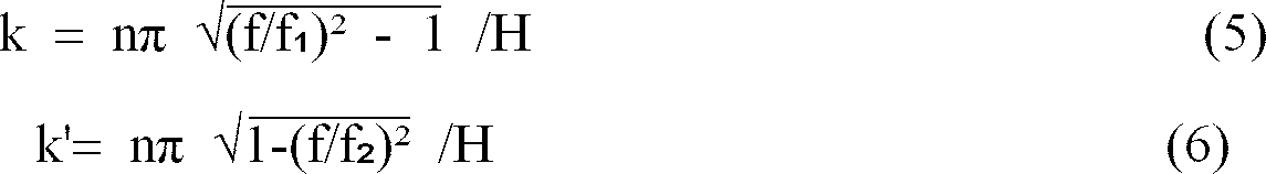
- In equations (1) through (6) described above, the following equation of frequency can be derived out from the boundary condition that the displacement and stress are continuous when


Let us determine an equation of approximation of equation (7) when f₁ is slightly lower than f₂. - Let us denote the observable frequency, that is the resonance frequency by f where the substrate thickness is varied in region (II) shown in Fig.2a or where electrodes are attached.
- Then two normalizing frequencies δ and Δ that satisfy the following equation are introduced.


This equation shows the relationship between the normalized resonance frequency Ψ utilizing b/a as a parameter and the resonator dimension na √
- The frequency spectra of the higher order symmetric and asymmetric mode vibrations where

- As can be clearly noted from Fig.2b, the degree of energy entrapping of the lowest order symmetric mode vibration varies greatly depending upon the dimension of the substrate, whereas the degree of entrapping higher order symmetric and asymmetric mode vibrations can be deemed substantially equal for the infinite area substrate and the limited area substrate.
- More particularly, the above-mentioned preconditions (2) and (3) can be applied to the limited area substrate as they are. When compared with the characteristic of the lowest order symmetric (S₀) mode, the inclinations of the other modes are steep and this tendency becomes remarkable as the mode becomes higher order. This characteristic too is retained in the limited area substrate.
- The above-mentioned facts (1) through (5) constitute the premise of invention,
Fig.3a through Fig.3c are sectional views showing the fundamental construction of the resonator according to this invention and graphs for explaining the principle of this invention. - As shown in Fig.3a,
electrodes 2 and 2' each having adiameter 2a are attached to both surfaces of the central portion of apiezoelectric substrate 1 having a thickness H for decreasing the cutoff frequency of the central portion to f₁ thereby providing a difference (f₂ - f₁) in the cutoff frequencies between the central portion and the surrounding portion having a cutoff frequency f₂. The portions at which theelectrodes 2 and 2' are attached are used as the vibration energy entrapping portions and theportions 3 and 3' not attached with electrodes are used as the vibration energy propagating portion of unwanted vibration. On the periphery of theportions 3 and 3' are formed vibrationenergy absorbing electrodes 4 and 4' having a cutoff frequency f₃(where f₃ < f₂). - When this resonator is used as an overtone vibration resonator of the fifth order, for example, the foregoing principle teaches that the percentage of the vibration energy entrapping the overtone vibration of the fundamental wave (first order) and of the third order should be small and that the entrapping percentage of the overtone vibration of the fifth and higher order should be large. For this reason, as shown in Fig.3b, the percentage T₅ of entrapping the vibration energy of the fifth order overtone vibration is set to about 80%, for example. As can be noted from Fig.3b, the entrapping coefficient na√


- When such material of high bonding property as lithium niobate, lithium tantalate or a piezoelectric ceramic is used as the piezoelectric substrate, as an extremely small amount of the electrode attached results in an extremely large frequency decrease, it is advantageous to vary the electrode size on the assumption that the amount of frequency decrease has already given.
- The cutoff frequency f₃ of the vibration
energy absorbing portions 4 and 4' may be the same as f₁, but if desired the frequency f₃ is increased or decreased thereby increasing, as far as possible, the consumption of the vibration energy in theportions 4 and 4'. - In the resonator manufactured as above described, the vibration energies of the fifth, seventh ... overtone oscillations are entrapped in the electrode portions as shown in Fig. 3c, the vibration energies of the overtone vibrations of the fundamental wave (first order) and the third order will not be entrapped in any appreciable amount, and these energies are leaked to the outer periphery of the piezoelectric substrate thereby causing the
piezoelectric substrate 1 to vibrate in the vibrationenergy absorbing portions 4 and 4'. Thus the energy is converted into heat in these portions and dissipated, the impedance of the lower order overtone vibrations including the fundamental vibration as viewed from the side of the oscillation circuit becomes higher than that of the higher order overtone vibration in which the energy is entrapped. This phenomenon can readily be understood if one imagines the energy distribution of the free electrode mounting portions of the so-called multimode piezoelectric monolithic filter in which a plurality of closely adjacent free electrodes are disposed between electrodes. - On the other hand, the overtone vibrations of the fifth order, seventh order ... overtone vibrations whose vibration energies are entrapped in the electrode portions as above described, since the vibration impedance of the fifth order is the minimum, this resonator is one in which the fifth order overtone vibration is the most easy to excite.
- When the lengths of the vibration
energy propagating portions 3 and 3' between the vibrationenergy entrapping portions 2 and 2' and the vibrationenergy absorbing portions 4 and 4' are extremely small, a portion of the entrapped vibration energy is consumed by the vibration energy absorbing portions. Conversely when the lengths are too large, the leakage energy propagate without any loss, so that theoretically, it can be deemed that the oscillation energy absorbing elements do not present as has been described above. - Accordingly, there must be optimum values for the lengths. However, as it is difficult to qualitatively determine the loss, let us determine the same by experiments. Fig. 4b shows the result of experiments when the vibration energy propagating gap is varied at the time of manufacturing a quartz resonator having the third order overtone vibration (50 MHz). When the gap (D-a) shown in Fig. 4a is too small, the impedance for the vibration of the fundamental wave (first order) and that for the third order overtone increases proportionally. Conversely, when the gap is too large, there is no difference among the impedances for the first and third overtone vibrations. Consequently, it was found that it is advantageous to select a value of about 1.5 for the ratio D/a so as to give a condition under which the third order overtone vibration is most easy to occur.
- The basic principle of this invention has been described hereinabove, actually, however, a resonator having a similar effect can be prepared even when the principle is more or less deviated.
- More particularly, as the frequency of an oscillation circuit increases, the gain of the amplifier decreases, the negative resistance of the circuit varies in reverse proportion to the square of the frequency. Accordingly, it is not always true that the oscillation at an overtone frequency at which the resonator impedance as seen from the side of the oscillation circuit becomes a minimum, is easiest.
- For example, in Fig.3b, when the percentage T of entrapping the vibration energy of the fifth order overtone vibration at a desired vibration frequency is set to a value, for example, about 60%, which is considerably lower than 80%. Qualitatively, the impedance for the seventh order overtone vibration may be somewhat smaller than the impedance for the fifth order overtone vibration. In such a case too, due to the characteristic of the oscillation circuit, the oscillating circuit does not oscillate at the seventh order overtone frequency at which the resonator impedance is the minimum, but at the fifth order overtone frequency the oscillation circuit may happen to oscillate.
- Accordingly, the term "desired overtone vibration" does not always mean an overtone vibration at which the resonator impedance as seen from the side of an oscillating circuit becomes minimum. Thus it is sufficient that the impedance at the "desired overtone vibration" is greatly smaller than that for the lower order overtone vibration including the fundamental wave vibration.
- The resonator that satisfies the conditions described above may have a plane configuration as shown in Figs. 6a - 6c.
- More particularly, as shown in Figs. 6a and 6b, main vibration
energy entrapping electrodes 2 and 2' are disposed at the central portion of apiezoelectric substrate 1,nonelectrode portions 3 and 3' (vibration energy propagating portions) are disposed about the electrodes, vibrationenergy absorbing electrodes 4 and 4' of a suitable configuration are disposed about the non-electrode portions, bothelectrodes lead wires 5 and 5' disposed bout the periphery of thesubstrate 1, and thevibration absorbing electrodes 4 and 4' are coupled together to have the same potential. - Thus, by connecting the vibrators and the circuit at the vibration energy absorbing electrode contacts, the electrodes can be utilized as tub electrodes so that the mechanical strength of the lead connections can be ensured.
- As shown in Fig.6c the lead pattern extending from the vibration energy entrapping portions may be directly connected to the vibration
energy absorbing electrodes 4 and 4' through the vibrationenergy propagating portions 3 and 3'. With this construction, however, it was experimentally confirmed that the desired overtone vibration energy too tends to slightly leak through thelead patterns 5 and 5'. However, this construction is advantageous in that since the lead wires are short, not only the ohmic loss can be reduced, but also the position alignment between the piezoelectric substrate and a vapor deposited pattern is not required to be accurate. - Furthermore, it is not always necessary to integrate the
lead wires 5 and 5' from the vibrationenergy entrapping electrodes 2 and 2' with the vibrationenergy absorbing electrodes 4 and 4', but instead they may be separated as shown in Fig.6d, or as shown in Fig. 6e, the vibrationenergy absorbing electrodes 4 and 4' may be formed to completely enclose the vibrationenergy entrapping portions 2 and 2'. This modified construction increases the consumption of the leakage energy thereby increasing the equivalent resistance for the vibration. - It should be understood that the construction of the resonator of this invention can be modified as shown in Figs. 7a through 7f.
- More particularly, in the constructions shown in Figs. 7a and 7b, the vibration energy propagating portion of the
piezoelectric substrate 1 are removed by etching, for example, on both or single surface, for increasing the cutoff frequency of these portions. This construction reduces the thickness of the attached electrodes which not only reduces the electrode vapor deposition time but also prevents peeling off of thick electrodes. - As the frequency is increased, the thickness of the main
vibration entrapping electrodes 2 and 2' becomes extremely thin whereby the electroconductivity is reduced and the performance of the electrode is lost. To obviate this problem, the portions of the piezoelectric substrate corresponding to the electrodes are slightly recessed as shown in Fig.7c for ensuring necessary electrode thickness. - It is not always necessary to attach the electrodes to the vibration energy absorbing portions on the outermost periphery of the piezoelectric substrate, but as shown in Fig.7d, the thickness of the substrate at that portion is increased for consuming unwanted vibration energy by thick end portions 4''.
- To attain the above described object, it is not always necessary to increase the thickness of the
piezoelectric substrate 1 at the outermost periphery, but a material having a large acoustic loss, for example, lead, tin, gold, etc. may be attached, ororganic materials - As shown in Fig.7f, a dot shaped
material electrodes 4,4' for consuming unwanted vibration energy. The resonator can be supported at said dot shaped material. - The result of experiment made on the characteristics of the resonator of this embodiment will be described in brief.
- In this experiment, a resonator having a construction as shown in Fig.4 and the following specification was used.
Quarts (AT cut) substrate dia. 7 mm Vibration frequency (overtone order) 50 MHz (third order) Vibration entrapping portion gold electrode, film thickness 350 Å electrode size 2mm x 2mm Gap between vibration entrapping electrode and absorbing electrode 0.5 mm Direction of arrangement of vibration energy absorbing electrode Z' direction - In this resonator, the CI values for the fundamental wave vibration and the third order overtone vibration are respectively 150Ω and 520Ω, while the CI value after bonding the lead wire to the resonator using an electroconductive bonding agent are respectively 280Ω and 53Ω which proves the correctness of the theory.
- Fig. 8a through 8c are sectional views showing another fundamental construction of a resonator of this invention utilizing the asymmetric mode and a graph for explaining the theory thereof. As shown in Fig.8a, split
electrodes piezoelectric substrate 1. When the resonator is excited, an asymmetric (a₀) vibration of the lowest order will be strongly excited. - Denoting the order of the overtone at which the resonator is desired to vibrate by n, where the parameters a and Δ are selected such that the position of the entrapping coefficient (n-2) a √


split electrodes 20,20'; and 30,30' as shown in Fig.8b, while the vibration energy of the overtone vibration of lower than (n-2)th order will spread over the entire surface of thepiezoelectric substrate 1 and a substantial amount of the energy will leak and consumed through the substrate supporting portion supporting the periphery of the substrate. - The vibration energy of the overtone vibration higher than the n-th order and entrapped near the peripheries of the
split electrodes - Fig.8c shows a basic method of selecting parameters where it is desired to obtain a third order overtone vibration resonator by utilizing an excitation of a₀ mode. The percentage T of entrapping the a₀ mode vibration energy becomes zero when the entrapping coefficient na
√

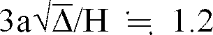
The spacing between the split electrodes may be selected to a suitable value so long as short circuiting does not occur between electrodes. Where the interelectrode spacing is extremely small, as is well known in the art, as a result of an acoustic coupling of the asymmetric mode vibration with a symmetric mode vibration which are simultaneously excited, two types of different vibration frequencies are generated. However, in the resonator of this embodiment, it is sufficient to derive out one of the frequencies, that is in this example only the resonance frequency of the asymmetric mode vibration, so that there is no problem. - Where it is desired to utilize the vibration of the higher mode, for example, S₁ mode or a₁ mode, each electrode is divided into three or four sections. In this case, as shown in Fig.2b, the gradient of each mode frequency spectrum becomes steeper as the order becomes higher so that this is advantageous because it is possible to set large the difference in the percentages of entrapping the n-th order overtone vibration energy and that of the order lower than (n-2)th order.
- In the above, the basic principle of this embodiment has been described. Actually, however, a resonator having similar performance can be obtained even when the principle is more or less deviated.
- More particularly, as the frequency of an oscillating circuit increases, the gain of its amplifier generally decreases so that the negative resistance of the circuit varies in reverse proportion to the square of the frequency. Accordingly, it is not always true that the vibration at an overtone frequency at which the resonator impedance as seen from the side of the oscillation circuit becomes a minimum is the most easy.
- For example, in Fig.8c for the purpose of manufacturing the fifth order overtone vibration resonator by utilizing the vibration of the lowest order asymmetric (a₀) mode vibration, when the parameters are selected such that the percentages of entrapping the vibration energies of the first order (fundamental wave vibration) and the third order overtone vibration are both zero, as shown in Fig.9, the percentage of entrapping the vibration energy of the fifth order overtone vibration will not become sufficiently large with the result that a case may occur in which the equivalent resistance for the fifth order overtone vibration is higher than that for the seventh order overtone vibration.
- In such a case, where the difference between the equivalent resistances for the fifth and seventh order overtone vibrations is small, it can be considered that the vibration of the fifth order overtone frequency is possible in view of the relation to the above described characteristic of the oscillation circuit. However, when the difference between the equivalent resistances for the fifth and seventh order overtone vibrations is large, the oscillating circuit may oscillate at the frequency of the seventh order overtone.
- In order to avoid this unstability, the percentage of entrapping the third order overtone vibration energy is made to be slightly larger than zero, and the percentage of entrapping the fifth order overtone vibration energy is selected such that the equivalent resistance for a desired fifth order overtone vibration becomes extremely smaller than that for the third order overtone vibration and that the equivalent resistance is slightly higher than that for the seventh order overtone vibration.
- It should be noted that, in this invention, it is not always necessary to make the vibration energy of an overtone vibration (including the fundamental wave vibration) of the order lower than the order of the overtone desired to vibration to be a perfectly not entrapped mode.
- In the foregoing, the invention was described by taking a case utilizing the lowest order asymmetric (a₀) mode vibration as an example, parameters a and Δ can be selected in the same manner as a case wherein a higher order asymmetric mode (a₁, a₂ ...) vibration or a higher order symmetric mode (S₁, S₂ ...) vibration.
- Having completed the description of the basic concept of this embodiment, the concrete electrode connection and wirings, necessary for manufacturing a resonator of this invention will be described in detail as follows.
- An electrode of a conventional resonator is required to be arranged for efficiently deriving out the charge created by the displacement of the piezoelectric substrate. As a consequence, in the resonator of this invention too, it is necessary to coincide the number and positions of the hills or valleys of the charge generated by the vibration mode utilized with those of the split electrode, and to interconnect such that the charges generated at respective electrodes will not cancel with each other.
- Where the vibration of the lowest order asymmetric (a₀) mode is to be utilized, as shown in Fig.10a, split
electrodes piezoelectric substrate 1 for generating electric charge having a level as shown in Fig.10b and the electrodes are connected in series as shown in Fig.10b or in parallel as shown in Fig.10c. Since the impedance of the parallel connection is 1/4 of that of the series connection, where it is desired to decrease the parallel resistance, parallel connection is preferred. - The spurious of a resonator utilizing a split electrode will now be considered. Where the utilized vibration mode is a higher order symmetric (S₁, S₂ ...) mode, an electrically asymmetric (a₀, a₁, a₂ ...) mode will not be excited, while where the vibration of a higher order asymmetric mode is to be utilized, the symmetric mode will not be excited. However, due to manufacturing errors of the resonator, some other modes are actually excited.
- Among the vibration modes utilized, a mode of different order, for example, a₂ mode with respect to a mode will be sufficiently excited.
- In the former case, however, the response is inherently very small and in the latter case the response is also small because the number of hills or valleys of the generated charge pattern does not coincide with the electrode division pattern so that the response is also small. In any case, the spurious caused by these facts does not reach a level causing a trouble.
- For the sake of reference, methods of connecting an electrode split into three sections and utilizing the S₁ mode are shown in Figs.11a and 11b.
- Examples of the wiring pattern to be formed on the piezoelectric substrate of a resonator utilizing an electrode split into two or more sections are shown in Figs. 12a through 12d. Figs. 12a and 12b show examples of series and parallel connections of the electrode split into two sections, while Figs. 12c and 12d show examples of series and parallel connections of the electrode split into 3 sections. Where the
wiring patterns 50 and 50' ---are made around the edge of the piezoelectric substrate, a conductor pattern is vapor deposited on edge too or an electroconductive point or bonding agent is coated for interconnecting the patterns on the front and rear surfaces. - Since the resonator of this embodiment is constructed to cause the vibration energy of an overtone vibration of the order lower than that of the desired overtone containing the fundamental wave vibration to leak and spread over the entire surface of the piezoelectric substrate, the leakage energy propagates without loss through portions of a large cutoff frequency thereby leaking out through a resonator support provided for the end of the piezoelectric substrate as described before.
- However, it is very important to consume the leakage energy effectively in order to increase the equivalent resistance of the vibration. For this purpose, a plurality of vibration
energy absorbing portions 60 having an extremely small cutoff frequency f₃ are provided on a part or the whole of the edge portion of thepiezoelectric substrate 1 as shown in Fig. 13a. With this construction, the amplitude of the leaking vibration energy is increased at this portion where the vibration energy is converted into thermal energy which is consumed thereat. Theenergy absorbing portions 60 may be provided either by thickening thepiezoelectric substrate 1 or by attaching a conduction film or a resin film of an appropriate mass. Alternatively, as shown in Fig. 13b, a mass such asadhesive agent 70 may be attached on the outer surface. - Although the cutoff frequency f₃ of the
energy absorbing portions 60 may be equal to or less than f₃, it is preferable to increase or decrease it so as to maximize the consumption of undesired vibration energy at this portion. - Further, in order to positively consume the leakage energy,
conductor films 8 may be attached at appropriate positions on the front and back surfaces of the edge portion of thepiezoelectric substrate 1 withresistors 9 connecting therebetween as shown in Fig. 13c. The resistance value r of the resistors can be basically determined as follows:
- fn
- : frequency of vibration to be converted into heat
- Co
- : capacitance between the conductor films provided on front and back surfaces.
- When there are a plurality of vibration frequencies whose energy is to be absorbed, a plurality of different resistors of (2πfa Co)⁻¹, (2πfb Co)⁻¹ --- can be applied to the periphery of the resonator. Alternatively, a resistors of (2πfm Co)⁻¹ may be applied where fm represents the mean value of fa, fb --- .
- The resistor is not necessarily to be limited to that utilized to construct an electronic circuit. For example, the resistor may take the form of a coating of an electroconductive bonding agent for fixing the support of a conventional quartz vibrator. This measure is advantageous in that it can be used without affecting the productivity of the resonator.
- Two different constructions of the overtone vibration resonator utilizing a lower order asymmetric (a₀) mode vibration and manufactured based on the principle described above and their characteristics will be described hereunder.
- Fig.14a shows a plan view of a basic third order overtone vibration resonator not provided with a vibration energy absorbing portion according to this invention. As shown,
lead wires 50 led out from themain electrode 20 and 20' split into two section are provided at the center of a circular quarts substrate for connecting in parallel, the front and rear electrodes having the same construction. - In Fig.14b, vibration
energy absorbing portions 60 are provided for the outer periphery of a quartz substrate. The results of measurement of the characteristics of these two types of resonators show that, in the former, the CI values of the third order and the first order (fundamental wave) overtone frequencies are 70Ω and 175Ω respectively. When a small quantity of an electroconductive bonding agent as applied these values become 72Ω and 380Ω respectively which proves the correctness of the theory of this invention. - The CI values of the third order and the first order (fundamental wave) overtone frequencies are 65Ω and 250Ω respectively. Where an electroconductive bonding agent is applied to the holder of the quartz substrate, these values become 65Ω and 1330Ω respectively, thus confirming the effectiveness of the vibration energy absorbing portion.
- In the resonator shown in Fig.14a, when the quartz substrate holder is fixed by the electroconductive bonding agent and then the electrode film thickness is varied. The difference between the CI values at the third order and the first order overtone frequencies decrease as shown in Fig.15a.
- This means that in the construction shown in Fig.12a, when Δ is caused to vary depending upon the electrode film thickness and both of the first order and the third order overtone vibrations are entrapped, the difference in the CI values decreases. Consequently, it will be clear that various parameters including the electrode film thickness should be set to maintain sufficiently large the difference between their CI values.
- Fig.15b shows the variation in the CI values at the first order and third order overtone frequencies where the gap between the exciting electrode and the energy absorbing portion of a resonator provided with the vibration energy absorbing portions shown in Fig.14b is varied.
- As can be noted, as the gap increases, the leaked vibration energy of the first order (fundamental wave) frequency is not sufficiently consumed by the energy absorbing portions thus decreasing the effect thereof. Accordingly, it is essential to set the gap between the energy absorbing portion and the exciting electrode to an optimum value.
- Since the construction of the resonator of this invention varies depending upon various requirements such as characteristic, manufacturing and frequency adjustment, the construction can be variously modified as shown in Figs. 16a through 16d.
- More particularly in the construction shown in Fig.16a, resin films 70' are applied to the vibration
energy absorbing portions 60 on the periphery of the piezoelectric substrate for decreasing the cutoff frequency of theportions 60. Fig.16b shows a construction in which, for the purpose of obtaining a sufficiently large cutoff frequency difference, the thicknesses of the substrate between themain electrodes energy absorbing portions 60 are reduced by etching for increasing the cutoff frequency thereof. Fig.16c shows a construction in which the thickness of the substrate is reduced between themain electrodes electrodes 80 are attached to the vibrationenergy absorbing portions 60. Thereby enabling electro-thermic conversion of the vibration energy. In Fig.16d, for the purpose of preventing increase in the electric resistance due to the decrease in the film thickness ofmain electrodes - The foregoing embodiments illustrate only few examples of the construction of the resonator of this invention, and if desired, suitable combinations of these constructions can be used.
- Although in the foregoing embodiment, a resonator utilizing the lowest order asymmetric (a₀) mode vibration and having simplest construction was described, it should be understood that the invention is not limited to this construction but can use higher order symmetric (S₁, S₂ ---) mode vibrations as well as higher order asymmetric mode vibrations.
- The vibration mode of an illustrated resonator is the lowest order asymmetric vibration mode of a quartz substrate excited in Z direction, but the quartz substrate can also be excited in X direction. Furthermore, it is possible to divide the electrode in Z and X directions for exciting vibrations in both directions.
- Although in Fig.14b, the vibration energy absorbing portions were provided in the Z direction, these portions can be provided in the X direction, or around substantially the entire periphery of the substrate or the portions can be divided into a plurality of sections. The vibration energy absorbing portions becomes more efficient as the area thereof covering the periphery of the substrate increases.
- The invention is not limited to a thickness twist vibration as shown in Figs. 14a and 14b but is also applicable to such vibration mode as thickness longitudinal and thickness slip vibrations. In addition, various types of the piezoelectric material can also be used.
- Although not shown in the drawing, the resonator may be a two port resonator having a three terminal electrode construction. This construction makes easy vibration in high frequency bands. When the invention is applied to a monolithic crystal filter, a filter characteristic having a small spurious over a wide frequency range can be expected.
- Fig.17 shows still another embodiment of this invention in which resistors R having suitable values are connected across
electrodes 4 and 4' on both surfaces of the energy absorbing portions near the outer periphery of the piezoelectric substrate. - With this modification, the vibration energy of an order lower than the desired overtone order propagates to the vibration energy absorbing portions excites the
piezoelectric substrate 1 at the vibration absorbing portions, and the electric charge generated in theelectrodes 4 and 4' is converted into heat energy by resistors R and then consumed, whereby the impedance for the lower order overtone vibration containing the fundamental wave vibration increases sufficiently. - The value of resistor R is set to be substantially equal to (2π fn Co)⁻¹ where Co represents the capacitance between
electrodes 4 and 4' and fn the frequency of the overtone vibration, the energy thereof is to be converted into heat and consumed. This condition corresponds to the impedance matching of an alternating current circuit so that it is a most efficient measure for absorbing unwanted vibration energy. - Where it is necessary to consume a plurality of vibration energies of the fundamental (first order) and the third order overtones such as the fifth order overtone vibration resonator, a frequency fm intermediate of the fundamental wave frequency fn1 and the third order overtone frequency fn3 is used for setting the value of resistor to

energy absorbing electrodes 4 and 4' are divided and resistors having values of
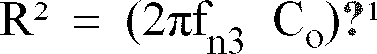
- Fig.19a is a plan view showing a modification based on this principle and Fig.19b is a sectional view of this modification taken along a line A-A. In this modification,
vibration enrapping electrodes 2 and 2' are provided for both surfaces at the center of aquartz substrate 1, and theelectrodes 2 and 2' are connected to vibrationenergy absorbing electrodes 4 and 4' at suitable portions on the outer periphery of thesubstrate 1 viapatterns 5 and 5'. - The
electrodes 4 and 4' are secured to resonator holdingportions 6 upwardly extending from a base, not shown, for supporting the resonator by using anelectroconductive bonding agent 7 for making electrical connection and mechanical fixing. - In this case, care should be taken not to short circuit the front and
rear electrodes 4 and 4' by theelectroconductive bonding agent 7. - By applying a
bonding agent 8 having a desired resistance value to suitable portions of theelectrodes 4 and 4', absorption of the unwanted vibration energy can be increased. - As the
bonding agent 8 can be used an epoxy resin containing a controlled quantity of dispersed carbon particles. - Where there are a plurality of wave motions whose vibration energies are to be absorbed, the vibration
energy absorbing electrodes 4 and the peripheral surface of thesubstrate 1 are split as shown in Fig.20, and thesplit electrodes resistive bonding agent 8 described above. Of course, the resistance value of the bonding agent should correspond to the frequency of the wave motions whose vibration energies are to be absorbed. - Figs. 21a and 21b show another resonator utilizing a composite material for use in a GHz band. As shown, boron (B) is doped into one surface of a
silicon block 500, and arecess 600 of a desired diameter is formed by etching the opposite surface. - Then a flat
thin layer 700 having a thickness equal to that of the layer doped with boron and cannot be etched will remain. Then alower electrode 800 and its lead wire are formed by vapor deposition. After that, Zn O₂ is sputtered to a desired thickness, and aupper electrode 100 and its lead electrode are vapor deposited on the film of Zn O₂. The portions covered by theelectrodes thin layer 700 extending about the outer peripheries of the electrodes is used as the vibration energy transmitting portion having a cutoff frequency f₂, and the not etchedportion 500 of the silicon block is used as a vibration energy absorbing portion having a cutoff frequency f₃. Then a relation f₃ > f₁ > f₂ holds automatically so that by suitably controlling the ratio between f₁ and f₂, the absolute value of f₂ and the diameters of theelectrodes - As is well known in the art as it is possible to manufacture extremely
thin layer 700 and sputtered ZnO, and hence having a high fundamental wave vibration frequency, it will be clear that it is possible to provide a high frequency oscillation circuit having 3, 5 or 7 times frequency and not requiring any special circuit, for example, a LC tuning circuit. - The resonator is not limited to a silicon block. Although the manufacturing steps becomes more or less complicated, as shown in Fig. 22, an opening having a desired diameter is formed at the center of an artificial quartz or
glass block 110 by mechanical machining or etching, and a quarts orglass plate 130 is strongly bonded to one surface of the block by a three layeralloy bonding agent 120 consisting of Aℓ-Ag-Jn. After lapping the quartz or glass plate to a desired thickness, upper andlower electrodes piezoelectric portion 900 made of Zn O and sandwitched between the upper and lower electrodes are formed. - Alternatively, an opening is formed through the central portion of a
metal block 140 as shown in Fig.23, and ametal plate 150 of the same material is seam welded to one surface of themetal block 140. Then themetal plate 150 is lapped to a desired thickness thereby forming a vibration portion. When such vibration portion is used as the vibration portion, it can be used as the lower electrode, the piezoelectric substrate can be directly sputtered onto thethin metal plate 150 and an insulatingfilm 160 is applied onto only the lead pattern wiring of the upper electrode attached to thepiezoelectric portion 900. Thereafter, the lead pattern is formed. - In addition to Zn O, Aℓ N and Cd S can also be used the piezoelectric material, and other method than sputtering can be used as the method of attaching the piezoelectric material. However, as the sputtering deposition method is most suitable for preparing extremely thin piezoelectric layer, this method can satisfy the object of this invention for preparing a resonator of an extremely high frequency. In this case, usually since the crystal grows in the axial direction, the vibration mode is limited to the thickness longitudinal vibration.
- Also, in this embodiment, a thickness slip vibration mode and a thickness twist vibration mode can be used.
- In the vibration
energy absorbing portion 4 shown in Fig.3a, the consumption of an overtone vibration on energy of an order lower than that of the desired overtone vibration after converting it into heat, is not sufficient as that the impedance at a corresponding frequency does not rise sufficiently. Thus a desired overtone vibration may become impossible in view of the negative resistance characteristic of the oscillation circuit as shown in Fig.24. - Accordingly, an experiment was carried out by using an overtone vibration resonator shown in Fig. 25 in which the amount of attaching the vibration
energy absorbing electrode 4 was varied for determining the difference between the CI value of the fundamental wave vibration and the CI value of the desired third order overtone vibration. - Fig.26 is a graph showing the result of experiment in which after fixing the size of the
exciting electrode 2 made of Ag, the film thickness is varied for varying the entrapping coefficient na√
energy absorbing electrodes 4 was varied to 1, 2, 4 and 8 times of that of the exciting electrode, and the relation between the CI value of the fundamental wave vibration to be suppressed and the CI value of the desired third order overtone vibration was plotted. - As can be noted from Fig.26, the CI value of the fundamental wave vibration to be suppressed has a peak value except a case wherein the ratio (film thickness ratio) between the thickness of the energy absorbing electrode mode of Ag and that of the excitation electrode is unify, the peak value increasing with the increase in the film thickness ratio.
- The same tendency was observed in the fifth order and the seventh order overtone vibration resonators although figures were omitted for the sake of simplicity.
- Above described result of experiment shows that it is necessary to make lower the cutoff frequency of the vibration energy absorbing portion than that of the vibration energy absorbing portion attached with an excitation electrode. Otherwise, it is impossible to have a sufficient difference between the CI value of the overtone vibration of an order at which the vibration is desired and that of the lower order overtone vibration containing the fundamental wave vibration to be suppressed, thus disenabling stable vibration at a desired frequency.
- When designing an overtone vibration piezoelectric resonator as shown in Fig.3a, it is essential to select the relation between a film thickness ratio at which the CI value for an overtone vibration of an order at which the vibration is desired to be extremely low while the CI value of the overtone vibration of a lower order including the fundamental wave vibration is extremely high, and the value of the entrapping coefficient by taking into consideration the result of experiment described above.
- The result of experiment shown in Fig.26 shows that optimum parameters for the third order overtone vibration resonator can be obtained when the film thickness ratio of the energy absorbing portion to the excitation electrode is selected to be 4 and the entrapping coefficient na√

- For decreasing the cutoff frequency of the vibration energy absorbing portion, it is not only possible to elongate only the vapor deposition time of a conductor to the portion, and to form a recess at the central portion of the
piezoelectric substrate 1 as shown in Figs. 27a through 27c for creating a difference between cutoff frequencies. Alternatively, as shown in Fig.27a, the same material a'' as the electrode can further be vapor deposited onto the vibrationenergy absorbing portion 400 thus formed. The cutoff frequency can be made more lower by using a vapor deposited material having a higher specific gravity than that of theelectrodes 2 and 2' (Fig. 27b). - Further, as shown in Fig.27c, for the purpose of obtaining a higher overtone vibration frequency, where the portions of the piezoelectric substrate on which the electrodes are to be attached are made particularly thin, it is sufficient to increase the thickness of the portions of the substrate which constitute the vibration energy absorbing portions.
- The cutoff frequency f₂ of the piezoelectric substrate about the
electrodes 2 and 2' is not always necessary to be perfectly the same on both surfaces and a slight difference is permissible. Even when the cutoff frequency f₃ of thevibration absorbing portions 400 at the periphery of the piezoelectric substrate varies substantially so long as the condition f₃ < f₁ is satisfied, there is no problem. - An electrode construction of the piezoelectric resonator will now be described that enables to compensate for the deterioration of the resonator characteristic caused by the deviation of the position of additional vapor deposition effected for the purpose of fine adjustment of the vibration frequency, and to greatly decrease the influence upon the resonator characteristic caused by the difference in the thickness of the piezoelectric substrate thereby increasing the upper limit of the resonance frequency.
- Fig.28a is a sectional view showing the fundamental construction of the electrode of such piezoelectric resonator.
- More particularly, a
surface electrode 2 is attached near the central portion of the surface of apiezoelectric substrate 1 and a rear electrode 2' having the same or wider area is attached to the rear surface, and the frequency is adjusted by applying an additional vapor deposition to the electrode 2'. - With this measure, even when the position of the additional vapor deposition for the fine adjustment of the frequency displaces a little, since the area of the additional vapor deposition is substantially wider than the area of the surface electrode, for example by about 1.5 times, there is no possibility of resulting in a new spurious. Even when the spurious is generated it is possible to limit it to an extremely low level, thereby causing no problem. Fig.28b shows a construction wherein the rear electrode 2' is extended to cover the entire rear surface of the piezoelectric substrate. This construction has the same advantage as that of the embodiment shown in Fig.28a. However, since the position of the vapor deposition mask utilized at the time of manufacturing the resonator may be rough, the construction shown in Fig.28b is advantageous from the point of produce ability.
- The piezoelectric vibrator having the electrode construction just described is advantageous for the following application.
- It is inevitable that the thickness of a piezoelectric substrate varies more or less during the manufacturing steps. In such case, in the prior art vibrator, the resonance frequency is matched by applying an additional vapor deposited film onto the surface electrode. This measure can eliminate variation in the resonance frequency, but since the amounts of plate back are different, the amount of entrapping the vibration energy is also different. As a consequence, the state of occurrence of the spurious caused thereby is different for respective vibrators.
- When this electrode construction is applied to such case, there arises an effect as shown in Figs. 29a and 29b.
- More particularly, when an additional
vapor deposition film 300 is added to the entire surface of the rear electrode 2' covering the entire rear surface as shown in Fig.29b for matching the resonance frequency to that of Fig.29a, the overall thickness of thepiezoelectric substrate 1 increases so that an effect equivalent to that obtained when the natural frequency of the substrate itself is adjusted. Consequently, not only the adjustment of resonance frequency of the resonator is possible but also vibrators of less variation in the characteristic can be mass produced. - This construction is advantageous for obtaining a resonator required to have a high resonance frequency.
- More particularly, when preparing a resonator described above, the electrode is desired to have a film thickness sufficient to provide a desired percentage of vibration energy entrapping. The parameter that governs the percentage of vibration energy entrapping is called an entrapping coefficient which is given by na √

- Where a resonator having a high resonance frequency is desired, the designer is requested to select parameters of the entrapping coefficient for obtaining desired energy entrapping percentage on a mode curve irrespective of what mode of vibration is used.
- There is an optimum value of the entrapping coefficient that minimizes accompanying auxiliary resonances.
- When investigating respective parameters of the entrapping coefficient, the substrate thickness H is substantially determined by the desired resonance frequency and the electrode size a is obliged to be determined to a predetermined value due to an equivalent inductance etc., so that only the remaining parameter, that is the amount of plate feed back, that is the electrode film thickness (sum of the surface and rear film thicknesses) presents a problem.
- As can be noted from the definition of the entrapping coefficient, the electrode film thickness becomes thin as the resonance frequency increases. Consequently, in the prior art vibrator, the thin electrode film is divided into equal sections on the front and rear surfaces, the respective sections can not act as the electrodes from the standpoint of electroconductivity. As is well known in the art, the thickness of the electrode film should be larger than 350 Å from the standpoint of electroconductivity irrespective whether what type of metal is used.
- Assuming that the film thickness of the surface electrode that determines the resonator characteristic, for example, the frequency of generating the auxiliary resonances is set near the limit of the electrode thickness, for example about 400 Å, this thickness determines the upper limit of the resonance frequency which is possible to design.
- Since the film thickness of the large are a electrode covering the entire rear surface has no influence upon such characteristic as the auxiliary resonance, the film thickness can be exclusively used to determine the frequency. For this reason, the thickness of the front and rear electrodes may be 400 Å and more. This measure enables to realize a piezoelectric resonator having a high resonance frequency which has been impossible in the past.
- A trially manufactured AT cut quartz vibrator had a substrate diameter of 5 mm, substrate thickness of 19 µm, a diameter of the surface and rear electrodes of 3 mm, a film thickness of 700 Å, a diameter of the surface electrode of 1.4 mm, a film thickness of 500 Å and a resonance frequency of 88 MHz. It was found that there was no problem of the auxiliary resonance.
- Assuming a diameter of 5 mm, a quartz substrate having a thickness of about 20 µm can be manufactured according to the present technique of polishing quartz. However, a resonator having diameter of 5 mm with electrodes of a thickness of about 500 Å close to the limit that satisfies the electrical characteristic attached to both surfaces of the substrate will have a substrate thickness of about 24 microns and its resonance frequency is limited to about 68 MHz. Thus, by using the electrode construction of this invention, the upper limit of the resonance frequency that has been considered possible can be increased by 30%.
- Furthermore this electrode construction is advantageous for the electrode of an overtone vibration piezoelectric vibrator requiring a delicate adjustment.
- Fig.30a is a plan view showing an overtone resonator resonator, which is the most fundamental resonator utilizing the lowest order symmetric (S₀) mode. As shown, a vibration energy entrapping
excitation electrode 2 is provided at the center of thepiezoelectric substrate 1 and leaked vibrationenergy absorbing electrodes 4 and 4' are attached to suitable positions on the outer periphery of the piezoelectric substrate, theelectrodes - In the prior art, the construction of the rear electrode is the same as that shown in Fig.30a.
- In an overtone resonator having above described electrode construction, unless the gap between the
exciting electrode 2 and the vibrationenergy absorbing portion 4 is maintained at a suitable value, that is when the gap is too large, the leaked vibration energy will not be consumed sufficiently. Consequently, when the gap is too small the vibration energy of a desired overtone vibration too is absorbed and consumed, thus disenabling vibration at the desired frequency. Consequently, where the position of the additional vapor deposition to theexcitation electrode 2 for the purpose of frequency adjustment becomes different, a serious problem occurs. - The problem described can be eliminated and the adjusting steps can be simplified by providing a
rear electrode 6 on the rear surface of the substrate, which covers both of theexcitation electrode 2 and the vibrationenergy absorbing portions 4, as shown in Fig.30b. - Since the overtone vibrating resonator of this invention is constructed to generate an overtone vibration (a high frequency vibration) by utilizing the inherent characteristic of the resonator without utilizing any special means, for example a LC tuning circuit, the fact that the fundamental frequency of the vibrator is high is a desirable characteristic. Accordingly, when the electrode construction just described is applied to this overtone vibrating vibrator not only the problem occurring at the time of adjusting the vibrator characteristic can be solved but also the resonance frequency of the resonator can be increased, which are extremely advantageous.
- In a resonator having a single
exciting electrode 2, whether the rear electrode 2' has a small area (Fig.31a) or a large area covering the entire rear surface (Fig.31b) it is necessary to lead out alead pattern 5. However, the relative size of the rear electrode 2' and thelead pattern 5 causes an unbalance of the mechanical vibration of the piezoelectric substrate. To alleviate such unbalance, abalancing pattern 5a acting as a counter balance weight is added to a suitable portion of the exciting electrode. - This construction can also be applied to a two port resonator wherein the exciting electrode is divided into a plurality of sections or to a dual mode filter having a similar electrode construction.
- Fig.32a shows the electrode construction when the present invention is applied to a two port vibrator or a dual mode filter. Fig.32b shows the electrode construction when the present invention is applied to an overtone vibration vibrator utilizing the lowest order asymmetrical (a₀) mode vibration, and Fig.32c shows the electrode construction when the present invention is applied to an overtone vibration vibrator utilizing a higher order symmetric (S₁) mode vibration
- With these electrode constructions, the problem of spurious caused by the displacement of the vapor deposition portion can be eliminated with simplified adjustment, etc. by merely varying the area or thickness of the electrode on the front or rear side of the vibrator. In addition, variation in the resonator characteristic caused by the variation in the percentage of vibration energy entrapping caused by the variation in the thickness of the piezoelectric substrate, when the vibration frequency thereof is adjusted.
- Moreover, as it is possible to increase the upper limit of the frequency of the resonator, it has an excellent temperature characteristic and capable acting as a frequency source for various-electronic apparatus and devices, the operating frequency increasing in recent years.
- Since the resonator of this invention is constructed as above described the resonator can readily generate an overtone frequency without changing the manufacturing steps of the prior art or without adding to the oscillation circuit any specific circuit, for example, a LC tuning circuit. Accordingly, the resonator of this invention can be advantageously used as a frequency source of various electronic apparatus and devices which are desired to operate at higher frequencies and to be constructed as integrated circuits of higher densities.
- Further in a conventional piezoelectric resonator, especially in such thickness vibration type resonator as an AT cut quartz resonator having an excellent temperature characteristic, when it is desired to obtain a high frequency at the fundamental wave vibration, the thickness of the piezoelectrics substrate becomes extremely small, thus making it difficult to manufacture. However, according to this invention, the resonator can be readily excited at an overtone frequency so that the thickness of the piezoelectric substrate can be selected in a range of ready manufacture thereby decreasing the manufacturing cost.
Claims (22)
- An overtone vibration piezoelectric resonator in which
a portion having a cutoff frequency f₂ is provided on a piezoelectric substrate (1) about an energy entrapping portion having a cutoff frequency f₁ (where f₁<f₂) so as to excite higher order mode vibrations,
among said vibrations, the vibration energy of an overtone vibration of an order above n-th order overtone vibration is substantially entrapped near the periphery of said energy entrapping portion,
parameters including the size of said energy entrapping portion, percentage of frequency decrease [(f₂-f₁)/f₂] and the thickness of said piezoelectric substrate (1) are selected such that the vibration energy of an overtone vibration of less than (n-2)th order including the fundamental wave vibration of the vibration of said mode is caused to spread over the entire surface of said piezoelectric substrate (1), thereby making easier the oscillation caused by said desired n-th order overtone vibration than the vibration caused by the overtone vibration of a lower order including fundamental wave vibration,
a vibration energy absorbing portion having a cutoff frequency smaller than said cutoff frequency f₂ is added to a given point near the outer periphery of said piezoelectric substrate (1) for efficiently consuming the vibration energy of an overtone vibration at an order lower than (n-2)th order overtone vibration including said fundamental wave vibration to be spread over the entire surface of said substrate (1),
characterized in that
the energy absorbing portions are provided with electrical electrodes (4,4';80). - The resonator as set forth in claim 1 wherein said energy entrapping portion comprises a single energy entrapping portion.
- The resonator as set forth in claim 1 wherein said energy entrapping portion is split into at least two sections.
- The resonator as set forth in one of claims 1-3 wherein said higher mode vibration comprises a symmetric mode vibration.
- The resonator as set forth in one of claims 1-3 wherein said higher order mode vibration comprises an asymmetric mode vibration.
- The resonator as set forth in one of claims 1-5 wherein excitation electrodes (2,2';20,20'; 30,30') and the energy absorbing portion are manufactured in a common process.
- The resonator as set forth in one of claims 1-6 wherein the excitation electrodes (2,2';20,20'; 30,30') and the energy absorbing portion are made of the same material.
- The resonator as set forth in one of claims 1-7 wherein a resistor (90) of a predetermined resistance value is connected across electrodes (80) attached to both surfaces near the outer periphery of said piezoelectric substrate (1), thereby increasing consumption of the vibration energy spread over the entire surface of said substrate (1).
- The resonator as set forth in claim 8 wherein the value of the resistor (90) connected across electrodes (80) which are attached to both surfaces of said vibration energy absorbing portion is made substantially equal to (2π fn Co)⁻¹ where Co represents the capacitance between said electrodes, and fn represents an overtone frequency whose vibration energy is to be absorbed.
- The resonator as set forth in claim 8 wherein the value of the resistor (90) connected across the electrodes (80) attached to the opposite surfaces of said vibration energy absorbing portion is made to be equal to (2π fm Co)⁻¹ where fm represents a predetermined frequency between a plurality of overtone frequencies including a fundamental wave vibration to be absorbed.
- The resonator as set forth in claim 8 wherein each of the electrodes (4) attached to both surfaces of said vibration energy absorbing portion is divided into a plurality of sections and the values of resistances connected across the electrode sections are made to be substantially equal to (2π fn1 Co)⁻¹, (2π fn3 Co)⁻¹ ... respectively where fn1,fn3,... represent a fundamental frequency and a third order overtone frequency ...
- The resonator as set forth in one of claims 1-11 wherein the cutoff frequency f₃ of said vibration energy absorbing portion is smaller than that f₁ of said vibration energy entrapping portion.
- The resonator as set forth in one of claims 1-11 wherein the cutoff frequency f₃ of said vibration energy absorbing portion is equal to the cutoff frequency f₁ of said vibration energy entrapping portion.
- The resonator as set forth in one of claims 1-13 wherein a surface electrode (2) of a predetermined area is attached near the central portion of said piezoelectric substrate (1) and a rear electrode (2') having a larger area than said surface electrode (2) is attached to the rear surface of said piezoelectric substrate (1) so as to decrease variation in the resonator characteristic caused by adjustment of the film thickness or the area of the electrode (2,2').
- The resonator as set forth in claim 14 wherein the rear electrode (2') covers the entire rear surface of the piezoelectric substrate (1).
- The resonator as set forth in claim 14 or 15 wherein said surface electrode (2) is divided into a plurality of sections.
- The resonator as set forth in one of claims 14-16 wherein a balance pattern having a mass corresponding to that of a lead pattern extending better said surface electrode and the periphery of said substrate (1) is provided for the surface of said piezoelectric substrate for balancing the vibration mode of said resonator.
- The resonator as set forth in one of claims 1-17 wherein the vibration absorbing electrodes (4,4') are electrically coupled together to have the same potential.
- The resonator as set forth in one of claims 1-18 wherein the vibration absorbing electrodes (4,4') enclose the vibration energy entrapping portions (2,2').
- A resonator, preferably as set forth in one of claims 1-19, wherein the relation of the frequencies of the vibration energy entrapping portion, the vibration energy propagating portion and the energy absorbing portion is influenced by etching the piezoelectric substrate.
- The resonator as set forth in claim 20 wherein the thickness of the vibration energy propagating portion is reduced compared with the thickness of the vibration energy entrapping portion by etching the piezoelectric substrate.
- The resonator as set forth in claim 20 wherein the thickness of the vibration energy entrapping portion is reduced compared with the thickness of the vibration energy propagating portion by etching the piezoelectric substrate.
Applications Claiming Priority (13)
| Application Number | Priority Date | Filing Date | Title |
|---|---|---|---|
| JP60077065A JPS61236208A (en) | 1985-04-11 | 1985-04-11 | Piezoelectric resonator for over-tone oscillation |
| JP77065/85 | 1985-04-11 | ||
| JP119055/85 | 1985-05-31 | ||
| JP60119055A JPS61277214A (en) | 1985-05-31 | 1985-05-31 | Electrode structure for piezoelectric resonator for overtone oscillation |
| JP9756/86 | 1986-01-20 | ||
| JP61009756A JP2640936B2 (en) | 1986-01-20 | 1986-01-20 | Piezoelectric resonator for overtone oscillation using higher-order mode vibration |
| JP61010826A JPH0777334B2 (en) | 1986-01-21 | 1986-01-21 | Piezoelectric resonator for overtone oscillation |
| JP10825/86 | 1986-01-21 | ||
| JP10826/86 | 1986-01-21 | ||
| JP10824/86 | 1986-01-21 | ||
| JP61010824A JPS62169508A (en) | 1986-01-21 | 1986-01-21 | Electrode structure for piezoelectric vibrator |
| JP61010825A JP2640937B2 (en) | 1986-01-21 | 1986-01-21 | Overtone oscillation piezoelectric resonator with composite structure |
| EP86902487A EP0220320B1 (en) | 1985-04-11 | 1986-04-11 | Piezo-electric resonator for generating overtones |
Related Parent Applications (1)
| Application Number | Title | Priority Date | Filing Date |
|---|---|---|---|
| EP86902487.7 Division | 1986-04-11 |
Publications (1)
| Publication Number | Publication Date |
|---|---|
| EP0680142A1 true EP0680142A1 (en) | 1995-11-02 |
Family
ID=27548225
Family Applications (2)
| Application Number | Title | Priority Date | Filing Date |
|---|---|---|---|
| EP86902487A Expired - Lifetime EP0220320B1 (en) | 1985-04-11 | 1986-04-11 | Piezo-electric resonator for generating overtones |
| EP95108355A Withdrawn EP0680142A1 (en) | 1985-04-11 | 1986-04-11 | Piezoelectric resonators for overtone oscillations |
Family Applications Before (1)
| Application Number | Title | Priority Date | Filing Date |
|---|---|---|---|
| EP86902487A Expired - Lifetime EP0220320B1 (en) | 1985-04-11 | 1986-04-11 | Piezo-electric resonator for generating overtones |
Country Status (5)
| Country | Link |
|---|---|
| US (1) | US4870313A (en) |
| EP (2) | EP0220320B1 (en) |
| KR (1) | KR920005610B1 (en) |
| DE (1) | DE3650562T2 (en) |
| WO (1) | WO1986006228A1 (en) |
Cited By (5)
| Publication number | Priority date | Publication date | Assignee | Title |
|---|---|---|---|---|
| GB2325336A (en) * | 1997-05-15 | 1998-11-18 | Tron Ind Inc M | Selected overtone resonator with two or more coupled resonant thicknesses |
| US6016025A (en) * | 1997-05-15 | 2000-01-18 | M-Tron Industries, Inc. | Selected overtone resonator with channels |
| CN1074213C (en) * | 1996-08-27 | 2001-10-31 | 株式会社村田制作所 | Piezoresonator and electronic element for using it |
| EP1170862A2 (en) | 2000-06-23 | 2002-01-09 | Murata Manufacturing Co., Ltd. | Piezoelectric resonator and piezoelectric filter using the same |
| WO2008034597A1 (en) * | 2006-09-21 | 2008-03-27 | Atmel Duisburg Gmbh | Integrated circuit arrangement and use of supply cables |
Families Citing this family (73)
| Publication number | Priority date | Publication date | Assignee | Title |
|---|---|---|---|---|
| DE3650562T2 (en) * | 1985-04-11 | 1997-03-20 | Toyo Communication Equip | PIEZOELECTRIC RESONATOR FOR GENERATING HARMONICS |
| US5345134A (en) * | 1988-06-29 | 1994-09-06 | Raytheon Company | Saw device and method of manufacture |
| JP2813996B2 (en) * | 1989-11-30 | 1998-10-22 | セイコープレシジョン株式会社 | 3rd overtone AT-cut crystal unit |
| US5112642A (en) * | 1990-03-30 | 1992-05-12 | Leybold Inficon, Inc. | Measuring and controlling deposition on a piezoelectric monitor crystal |
| US5668057A (en) * | 1991-03-13 | 1997-09-16 | Matsushita Electric Industrial Co., Ltd. | Methods of manufacture for electronic components having high-frequency elements |
| US5747857A (en) * | 1991-03-13 | 1998-05-05 | Matsushita Electric Industrial Co., Ltd. | Electronic components having high-frequency elements and methods of manufacture therefor |
| JPH06291587A (en) * | 1992-07-08 | 1994-10-18 | Matsushita Electric Ind Co Ltd | Piezoelectric vibrator |
| US5446429A (en) * | 1993-04-08 | 1995-08-29 | Murata Mfg. Co., Ltd. | Piezoelectric vibrator for reduction of undesired vibrations |
| US5455475A (en) * | 1993-11-01 | 1995-10-03 | Marquette University | Piezoelectric resonant sensor using the acoustoelectric effect |
| US5495135A (en) * | 1994-09-21 | 1996-02-27 | Motorola, Inc. | Piezoelectric resonator with an attenuated spurious response |
| JP3432321B2 (en) * | 1995-01-31 | 2003-08-04 | 太平洋セメント株式会社 | Multilayer ceramic piezoelectric element |
| US5705201A (en) * | 1995-09-01 | 1998-01-06 | Ibar; Jean-Pierre | Apparatus for controlling gas assisted injection molding to produce hollow and non-hollow plastic parts and modify their physical characteristics |
| US5869763A (en) * | 1995-10-19 | 1999-02-09 | The United States Of America As Represented By The Secretary Of The Army | Method for measuring mass change using a quartz crystal microbalance |
| FR2745667B1 (en) * | 1996-03-01 | 1998-05-22 | Ecole Nale Sup Artes Metiers | PIEZOELECTRIC RESONATOR WITH SELECTIVE EXCITATION |
| EP0818882A3 (en) * | 1996-07-10 | 1999-12-15 | Matsushita Electric Industrial Co., Ltd. | Energy trapping piezoelectric device and producing method thereof |
| JPH1098350A (en) * | 1996-07-31 | 1998-04-14 | Daishinku Co | Piezoelectric vibrating device |
| JP3262007B2 (en) * | 1997-01-10 | 2002-03-04 | 株式会社村田製作所 | Energy trap type thickness-slip resonator and electronic components using this resonator |
| US5939815A (en) * | 1997-07-23 | 1999-08-17 | The United States Of America As Represented By The Secretary Of The Army | Field trapping electrodes |
| JPH11168343A (en) * | 1997-12-04 | 1999-06-22 | Murata Mfg Co Ltd | Thickness vertical piezoelectric resonator |
| EP1078453B1 (en) | 1998-05-08 | 2003-04-16 | Infineon Technologies AG | Thin-layered piezo-resonator |
| JP2000134060A (en) * | 1998-10-26 | 2000-05-12 | Murata Mfg Co Ltd | Energy confinement type piezoelectric resonator, and energy confinement type piezoelectric resonator component |
| JP2000252786A (en) * | 1999-03-01 | 2000-09-14 | Matsushita Electric Ind Co Ltd | Piezoelectric vibrating element |
| DE19914468C1 (en) * | 1999-03-30 | 2000-09-07 | Siemens Ag | Piezo-resonator, used as signal filter, impedance matcher and transformer of mobile telecommunications device, has pairs of interdigital electrodes of finger size less than the produced HF mechanical vibration wavelength |
| JP3317274B2 (en) * | 1999-05-26 | 2002-08-26 | 株式会社村田製作所 | Surface acoustic wave device and method of manufacturing surface acoustic wave device |
| FI107660B (en) * | 1999-07-19 | 2001-09-14 | Nokia Mobile Phones Ltd | resonator |
| JP2001144576A (en) * | 1999-11-12 | 2001-05-25 | Murata Mfg Co Ltd | Piezoelectric resonator |
| JP2001144577A (en) * | 1999-11-15 | 2001-05-25 | Murata Mfg Co Ltd | Piezoelectric resonator |
| FR2806225B1 (en) * | 2000-03-10 | 2006-12-29 | Sagem | VIBRATION MOTORS |
| CN1459128A (en) * | 2000-07-17 | 2003-11-26 | 长浦善昭 | Piezoelectric device and acousto-electric transducer and method for manufacturing the same |
| JP2002299998A (en) * | 2001-04-02 | 2002-10-11 | Matsushita Electric Ind Co Ltd | Piezoelectric vibrator and piezoelectric filter |
| JP2002368571A (en) * | 2001-06-11 | 2002-12-20 | Matsushita Electric Ind Co Ltd | Piezoelectric vibrator and filter using the same |
| JP3954395B2 (en) * | 2001-10-26 | 2007-08-08 | 富士通株式会社 | Piezoelectric thin film resonator, filter, and method of manufacturing piezoelectric thin film resonator |
| WO2004001849A2 (en) * | 2002-04-30 | 2003-12-31 | Hrl Laboratories, Llc | Quartz-based nanoresonators and method of fabricating same |
| WO2004001964A1 (en) * | 2002-06-20 | 2003-12-31 | Ube Industries, Ltd. | Thin film piezoelectric oscillator, thin film piezoelectric device, and manufacturing method thereof |
| JP4215717B2 (en) * | 2002-07-19 | 2009-01-28 | シーメンス アクチエンゲゼルシヤフト | Device for detecting substance and method for detecting substance |
| SE0300375D0 (en) | 2003-02-12 | 2003-02-12 | Attana Ab | Piezoelectric resonator |
| US8766745B1 (en) | 2007-07-25 | 2014-07-01 | Hrl Laboratories, Llc | Quartz-based disk resonator gyro with ultra-thin conductive outer electrodes and method of making same |
| US7994877B1 (en) | 2008-11-10 | 2011-08-09 | Hrl Laboratories, Llc | MEMS-based quartz hybrid filters and a method of making the same |
| JP4222513B2 (en) * | 2003-08-19 | 2009-02-12 | 日本碍子株式会社 | Mass measuring apparatus and method |
| ATE515108T1 (en) * | 2003-09-12 | 2011-07-15 | Panasonic Corp | TUNABLE THIN FILM VOLUME WAVE RESONATOR, PRODUCTION METHOD THEREOF, FILTER, MULTI-LAYER COMPOSITE ELECTRONIC COMPONENT AND COMMUNICATION DEVICE |
| US6903629B1 (en) * | 2003-09-24 | 2005-06-07 | The United States Of America As Represented By The Secretary Of The Army | Electrode-free resonator structures for frequency control, filters and sensors |
| KR100662865B1 (en) * | 2003-10-08 | 2007-01-02 | 삼성전자주식회사 | Film bulk acoustic resonator and the method for manufacturing the same |
| JP4434082B2 (en) * | 2004-09-07 | 2010-03-17 | 株式会社村田製作所 | Method for manufacturing piezoelectric resonator |
| JP3838260B2 (en) * | 2004-10-14 | 2006-10-25 | 株式会社村田製作所 | Energy-confined piezoelectric resonator |
| WO2006062082A1 (en) * | 2004-12-07 | 2006-06-15 | Matsushita Electric Industrial Co., Ltd. | Thin film elastic wave resonator |
| JPWO2006062083A1 (en) * | 2004-12-07 | 2008-06-12 | 松下電器産業株式会社 | Thin film acoustic wave resonator |
| US7568377B2 (en) * | 2005-07-28 | 2009-08-04 | University Of South Florida | High frequency thickness shear mode acoustic wave sensor for gas and organic vapor detection |
| US7183698B1 (en) * | 2005-08-29 | 2007-02-27 | Zippy Technology Corp. | Piezoelectric structure |
| US7185695B1 (en) * | 2005-09-01 | 2007-03-06 | United Technologies Corporation | Investment casting pattern manufacture |
| DE102005043034A1 (en) * | 2005-09-09 | 2007-03-15 | Siemens Ag | Apparatus and method for moving a liquid |
| US7555824B2 (en) | 2006-08-09 | 2009-07-07 | Hrl Laboratories, Llc | Method for large scale integration of quartz-based devices |
| US7884930B2 (en) * | 2007-06-14 | 2011-02-08 | Hrl Laboratories, Llc | Integrated quartz biological sensor and method |
| US10266398B1 (en) | 2007-07-25 | 2019-04-23 | Hrl Laboratories, Llc | ALD metal coatings for high Q MEMS structures |
| US8151640B1 (en) | 2008-02-05 | 2012-04-10 | Hrl Laboratories, Llc | MEMS on-chip inertial navigation system with error correction |
| US7802356B1 (en) | 2008-02-21 | 2010-09-28 | Hrl Laboratories, Llc | Method of fabricating an ultra thin quartz resonator component |
| US8487719B2 (en) * | 2008-04-29 | 2013-07-16 | Triquint Semiconductor, Inc. | Bulk acoustic wave resonator |
| US8349611B2 (en) * | 2009-02-17 | 2013-01-08 | Leversense Llc | Resonant sensors and methods of use thereof for the determination of analytes |
| US8176607B1 (en) | 2009-10-08 | 2012-05-15 | Hrl Laboratories, Llc | Method of fabricating quartz resonators |
| US8912711B1 (en) | 2010-06-22 | 2014-12-16 | Hrl Laboratories, Llc | Thermal stress resistant resonator, and a method for fabricating same |
| US9250074B1 (en) | 2013-04-12 | 2016-02-02 | Hrl Laboratories, Llc | Resonator assembly comprising a silicon resonator and a quartz resonator |
| JP2014212409A (en) * | 2013-04-18 | 2014-11-13 | セイコーエプソン株式会社 | Mems vibrator, electronic apparatus and movable object |
| US9599470B1 (en) | 2013-09-11 | 2017-03-21 | Hrl Laboratories, Llc | Dielectric high Q MEMS shell gyroscope structure |
| US9977097B1 (en) | 2014-02-21 | 2018-05-22 | Hrl Laboratories, Llc | Micro-scale piezoelectric resonating magnetometer |
| US9991863B1 (en) | 2014-04-08 | 2018-06-05 | Hrl Laboratories, Llc | Rounded and curved integrated tethers for quartz resonators |
| JP2016019225A (en) * | 2014-07-10 | 2016-02-01 | 富士通株式会社 | Crystal oscillator |
| US10308505B1 (en) | 2014-08-11 | 2019-06-04 | Hrl Laboratories, Llc | Method and apparatus for the monolithic encapsulation of a micro-scale inertial navigation sensor suite |
| US9791503B1 (en) * | 2015-09-30 | 2017-10-17 | Integrated Device Technology, Inc. | Packaged oscillators with built-in self-test circuits that support resonator testing with reduced pin count |
| US10031191B1 (en) | 2015-01-16 | 2018-07-24 | Hrl Laboratories, Llc | Piezoelectric magnetometer capable of sensing a magnetic field in multiple vectors |
| US9503045B2 (en) | 2015-01-19 | 2016-11-22 | Seiko Epson Corporation | Resonator element, resonator, oscillator, electronic apparatus, and moving object |
| US10110198B1 (en) | 2015-12-17 | 2018-10-23 | Hrl Laboratories, Llc | Integrated quartz MEMS tuning fork resonator/oscillator |
| US10175307B1 (en) | 2016-01-15 | 2019-01-08 | Hrl Laboratories, Llc | FM demodulation system for quartz MEMS magnetometer |
| CN111010100A (en) * | 2019-03-02 | 2020-04-14 | 天津大学 | Bulk acoustic wave resonator with piezoelectric layer having recessed structure, filter, and electronic device |
| CN111786636A (en) * | 2020-07-24 | 2020-10-16 | 苏州汉天下电子有限公司 | Tunable resonator and method of manufacturing the same |
Citations (3)
| Publication number | Priority date | Publication date | Assignee | Title |
|---|---|---|---|---|
| US3382381A (en) * | 1965-05-27 | 1968-05-07 | Piezo Technology Inc | Tab plateback |
| DE2641571B1 (en) * | 1976-09-15 | 1977-06-08 | Siemens Ag | THICK SHEAR VIBRATORS USED AS OBSERVE QUARTZ |
| GB2020898A (en) * | 1978-04-05 | 1979-11-21 | Citizen Watch Co Ltd | Piezoelectric vibrator |
Family Cites Families (20)
| Publication number | Priority date | Publication date | Assignee | Title |
|---|---|---|---|---|
| FR439666A (en) * | 1912-02-02 | 1912-06-20 | Gilbert Bougnol | Improvements in the construction of fencing weapons, épées, foils and sabers |
| US2249933A (en) * | 1938-09-24 | 1941-07-22 | Telefunken Gmbh | Piezoelectric plate |
| US3495105A (en) * | 1967-07-19 | 1970-02-10 | Ngk Spark Plug Co | Three-terminal piezoelectric resonator |
| US3384768A (en) * | 1967-09-29 | 1968-05-21 | Clevite Corp | Piezoelectric resonator |
| US3747176A (en) * | 1969-03-19 | 1973-07-24 | Murata Manufacturing Co | Method of manufacturing an energy trapped type ceramic filter |
| US3585418A (en) * | 1969-07-22 | 1971-06-15 | Clevite Corp | Piezoelectric resonators and method of tuning the same |
| AU448240B2 (en) * | 1970-06-18 | 1974-04-19 | Amalgamated Wireless (Australia) Ltd | Quartz crystals |
| US3699484A (en) * | 1970-06-24 | 1972-10-17 | Vernitron Corp | Width extensional resonator and coupled mode filter |
| US3684905A (en) * | 1971-04-15 | 1972-08-15 | Mccoy Electronics Co | Piezoelectric crystal device including loading elements having the shape of chordal sections |
| JPS515196A (en) * | 1974-07-02 | 1976-01-16 | Takeshi Uchida | JODOME SOCHI |
| DE2516307A1 (en) * | 1975-04-15 | 1976-10-28 | Licentia Gmbh | Quartz crystal oscillator element - has high frequency stability over whole of life span |
| US4365181A (en) * | 1979-07-18 | 1982-12-21 | Murata Manufacturing Co., Ltd. | Piezoelectric vibrator with damping electrodes |
| US4381469A (en) * | 1979-07-20 | 1983-04-26 | Murata Manufacturing Company, Ltd. | Temperature stable piezoelectric device |
| GB2069752A (en) * | 1980-02-06 | 1981-08-26 | Gen Electric Co Ltd | Piezoelectric resonators |
| JPS5831609A (en) * | 1981-08-19 | 1983-02-24 | Nec Corp | Thin film piezoelectric oscillator |
| JPS58137317A (en) * | 1982-02-09 | 1983-08-15 | Nec Corp | Thin-film piezoelectric compound oscillator |
| JPS58175314A (en) * | 1982-03-11 | 1983-10-14 | Nec Corp | Thin film piezoelectric oscillator |
| US4502932A (en) * | 1983-10-13 | 1985-03-05 | The United States Of America As Represented By The United States Department Of Energy | Acoustic resonator and method of making same |
| DE3650562T2 (en) * | 1985-04-11 | 1997-03-20 | Toyo Communication Equip | PIEZOELECTRIC RESONATOR FOR GENERATING HARMONICS |
| JPH05336494A (en) * | 1992-05-28 | 1993-12-17 | Mitsubishi Electric Corp | Recording medium, recording device, and reproducing device |
-
1986
- 1986-04-11 DE DE3650562T patent/DE3650562T2/en not_active Expired - Fee Related
- 1986-04-11 KR KR1019860700886A patent/KR920005610B1/en not_active IP Right Cessation
- 1986-04-11 WO PCT/JP1986/000181 patent/WO1986006228A1/en active IP Right Grant
- 1986-04-11 EP EP86902487A patent/EP0220320B1/en not_active Expired - Lifetime
- 1986-04-11 EP EP95108355A patent/EP0680142A1/en not_active Withdrawn
-
1988
- 1988-05-09 US US07/191,628 patent/US4870313A/en not_active Expired - Lifetime
Patent Citations (3)
| Publication number | Priority date | Publication date | Assignee | Title |
|---|---|---|---|---|
| US3382381A (en) * | 1965-05-27 | 1968-05-07 | Piezo Technology Inc | Tab plateback |
| DE2641571B1 (en) * | 1976-09-15 | 1977-06-08 | Siemens Ag | THICK SHEAR VIBRATORS USED AS OBSERVE QUARTZ |
| GB2020898A (en) * | 1978-04-05 | 1979-11-21 | Citizen Watch Co Ltd | Piezoelectric vibrator |
Non-Patent Citations (1)
| Title |
|---|
| J. BIRCH ET AL.: "Appraisal of the inverted-mesa AT-cut quartz resonator for achieving low-inductance high-Q single-response crystal units", ELECTRONICS LETTERS, vol. 15, no. 20, 27 September 1979 (1979-09-27), STEVENAGE GB, pages 641 - 643, XP002119273 * |
Cited By (7)
| Publication number | Priority date | Publication date | Assignee | Title |
|---|---|---|---|---|
| CN1074213C (en) * | 1996-08-27 | 2001-10-31 | 株式会社村田制作所 | Piezoresonator and electronic element for using it |
| GB2325336A (en) * | 1997-05-15 | 1998-11-18 | Tron Ind Inc M | Selected overtone resonator with two or more coupled resonant thicknesses |
| US6016025A (en) * | 1997-05-15 | 2000-01-18 | M-Tron Industries, Inc. | Selected overtone resonator with channels |
| EP1170862A2 (en) | 2000-06-23 | 2002-01-09 | Murata Manufacturing Co., Ltd. | Piezoelectric resonator and piezoelectric filter using the same |
| EP1170862A3 (en) * | 2000-06-23 | 2002-02-13 | Murata Manufacturing Co., Ltd. | Piezoelectric resonator and piezoelectric filter using the same |
| US6556103B2 (en) | 2000-06-23 | 2003-04-29 | Murata Manufacturing Co., Ltd. | Piezoelectric resonator with electrode radius related to resonator thickness and vibration mode, and filter using the same |
| WO2008034597A1 (en) * | 2006-09-21 | 2008-03-27 | Atmel Duisburg Gmbh | Integrated circuit arrangement and use of supply cables |
Also Published As
| Publication number | Publication date |
|---|---|
| KR880700541A (en) | 1988-03-15 |
| EP0220320A1 (en) | 1987-05-06 |
| DE3650562D1 (en) | 1996-10-02 |
| DE3650562T2 (en) | 1997-03-20 |
| US4870313A (en) | 1989-09-26 |
| KR920005610B1 (en) | 1992-07-09 |
| WO1986006228A1 (en) | 1986-10-23 |
| EP0220320B1 (en) | 1996-08-28 |
| EP0220320A4 (en) | 1988-10-05 |
Similar Documents
| Publication | Publication Date | Title |
|---|---|---|
| EP0680142A1 (en) | Piezoelectric resonators for overtone oscillations | |
| US9948275B2 (en) | Piezoelectric vibration element, piezoelectric vibrator, piezoelectric oscillator, and electronic device | |
| EP1557945B1 (en) | Piezoelectric vibrator, filter using same, and method for adjusting piezoelectric vibrator | |
| US4365181A (en) | Piezoelectric vibrator with damping electrodes | |
| US20020089261A1 (en) | Surface mount quartz crystal resonators and methods for making same | |
| EP1079522A1 (en) | Piezoelectric vibration device | |
| JP2013042440A (en) | Piezoelectric vibrating element, piezoelectric vibrator, electronic device and electronic apparatus | |
| JPH0435108A (en) | Ultra thin plate multiple mode crystal filter element | |
| JPH11284484A (en) | Uhf band fundamental frequency crystal oscillator and its filter | |
| JP2013046085A (en) | Piezoelectric vibration element, piezoelectric vibrator, electronic device, and electronic device | |
| JP4003302B2 (en) | Piezoelectric vibrator | |
| JP3262007B2 (en) | Energy trap type thickness-slip resonator and electronic components using this resonator | |
| JP2013042410A (en) | Piezoelectric vibrating element, piezoelectric vibrator, electronic device and electronic apparatus | |
| US6967432B2 (en) | Piezoelectric shear resonator, composite piezoelectric shear resonator, and piezoelectric resonator component | |
| JP4196641B2 (en) | Ultra-thin piezoelectric device and manufacturing method thereof | |
| EP0468051A1 (en) | Structure of ultra-thin sheet piezoresonator | |
| JP2000040938A (en) | Ultra high frequency piezoelectric device | |
| JP3896585B2 (en) | Tuning fork type piezoelectric vibrator | |
| JP2640936B2 (en) | Piezoelectric resonator for overtone oscillation using higher-order mode vibration | |
| US6016025A (en) | Selected overtone resonator with channels | |
| JP2001257560A (en) | Electrode structure for ultra-thin board piezoelectric vibration element | |
| JP4325178B2 (en) | Piezoelectric vibration element, piezoelectric vibrator and piezoelectric oscillator | |
| JP2002368573A (en) | Superthin sheet piezoelectric vibrator and production method therefor | |
| JPH0124368B2 (en) | ||
| JP2001326554A (en) | Piezoelectric vibrator |
Legal Events
| Date | Code | Title | Description |
|---|---|---|---|
| PUAI | Public reference made under article 153(3) epc to a published international application that has entered the european phase |
Free format text: ORIGINAL CODE: 0009012 |
|
| 17P | Request for examination filed |
Effective date: 19950601 |
|
| AC | Divisional application: reference to earlier application |
Ref document number: 220320 Country of ref document: EP |
|
| AK | Designated contracting states |
Kind code of ref document: A1 Designated state(s): CH DE FR GB IT LI |
|
| RIN1 | Information on inventor provided before grant (corrected) |
Inventor name: TANAKA, YOSHIAKI, C/O TOYO COMM. EQUIP. CO., LTD. Inventor name: SHOUZI, TOMOKAZU, C/O TOYO COMM. EQUIP. CO., LTD. Inventor name: HIRAMA, KOUICHI, C/O TOYO COMM. EQUIP. CO., LTD. |
|
| 17Q | First examination report despatched |
Effective date: 19990225 |
|
| STAA | Information on the status of an ep patent application or granted ep patent |
Free format text: STATUS: THE APPLICATION IS DEEMED TO BE WITHDRAWN |
|
| 18D | Application deemed to be withdrawn |
Effective date: 19990708 |