EP0678756B1 - Staring focal plane array architecture for multiple applications - Google Patents
Staring focal plane array architecture for multiple applications Download PDFInfo
- Publication number
- EP0678756B1 EP0678756B1 EP95105825A EP95105825A EP0678756B1 EP 0678756 B1 EP0678756 B1 EP 0678756B1 EP 95105825 A EP95105825 A EP 95105825A EP 95105825 A EP95105825 A EP 95105825A EP 0678756 B1 EP0678756 B1 EP 0678756B1
- Authority
- EP
- European Patent Office
- Prior art keywords
- frame buffer
- focal plane
- plane array
- detector
- elements
- Prior art date
- Legal status (The legal status is an assumption and is not a legal conclusion. Google has not performed a legal analysis and makes no representation as to the accuracy of the status listed.)
- Expired - Lifetime
Links
Images
Classifications
-
- G—PHYSICS
- G06—COMPUTING OR CALCULATING; COUNTING
- G06F—ELECTRIC DIGITAL DATA PROCESSING
- G06F3/00—Input arrangements for transferring data to be processed into a form capable of being handled by the computer; Output arrangements for transferring data from processing unit to output unit, e.g. interface arrangements
- G06F3/14—Digital output to display device ; Cooperation and interconnection of the display device with other functional units
- G06F3/153—Digital output to display device ; Cooperation and interconnection of the display device with other functional units using cathode-ray tubes
-
- H—ELECTRICITY
- H04—ELECTRIC COMMUNICATION TECHNIQUE
- H04N—PICTORIAL COMMUNICATION, e.g. TELEVISION
- H04N5/00—Details of television systems
- H04N5/222—Studio circuitry; Studio devices; Studio equipment
- H04N5/262—Studio circuits, e.g. for mixing, switching-over, change of character of image, other special effects ; Cameras specially adapted for the electronic generation of special effects
- H04N5/2628—Alteration of picture size, shape, position or orientation, e.g. zooming, rotation, rolling, perspective, translation
-
- H—ELECTRICITY
- H04—ELECTRIC COMMUNICATION TECHNIQUE
- H04N—PICTORIAL COMMUNICATION, e.g. TELEVISION
- H04N5/00—Details of television systems
- H04N5/30—Transforming light or analogous information into electric information
- H04N5/33—Transforming infrared radiation
Definitions
- This invention relates to an infra red focal plane staring array which is capable of multiple applications and, more specifically, to a novel architecture for such focal plane staring arrays.
- Focal plane staring arrays are generally (see for example US-A-3 806 729) composed of a matrix of plural detector elements, each of the detector elements having an associated circuit with a capacitor which is charged in proportion to the amount of energy impinging thereon. Signals indicative of the charges on each of the capacitors in the array are read out, generally in serial manner, so that one detector element is being read out while the capacitor associated with the next detector element is being charged up. The capacitors are then again charged in accordance with the amount of energy impinging thereon and later read out. This procedure is repeated, generally on a timed basis. The outputs from the capacitors are therefore not simultaneously available or are not available in any manner such that the signals from predetermined ones of the detectors can be selected for operation on those signals only in some predetermined manner.
- the ability to "window" or output only a subarea of the focal plane array or only predetermined ones of the detectors of the focal plane array is advantageous.
- Multiple windowing or the ability to output upon request multiple subareas of the array is advantageous for tracking multiple targets in a large field of view.
- Another feature that is desirable is electronic dezoom to reduce data rates on large targets. Electronic dezoom combines adjacent detectors into one. That is, for a 2:1 dezoom, four detectors are combined into one. A 256 x 256 array becomes a 128 x 128 array. For missile seeker and other applications, it is desirable to change these features at will so that the sensor can adapt to the scenario at hand.
- a staring focal plane array architecture which uses a frame buffer to store detector samples.
- the frame buffer is basically one sample and hold circuit associated with each detector element. Once the samples from the focal plane detector are transferred to and stored in the frame buffer, this transfer being accomplished either serially, in parallel or some combination thereof, the data stored in the frame buffer can be read out in any order or any portion thereof can be read out to allow windowing. The samples are output in a non-destructive manner and retained until the next set of samples from the focal plane array is about to be transferred so that multiple areas can be output to allow multiple windows.
- the frame buffer can be built in a separate silicon chip but will be in close mechanical proximity to the chip containing the detectors and be electrically connected to this chip.
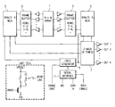
- FIGURE 1 there is shown a block diagram for a focal plane array that utilizes a frame buffer external to the focal plane array and the unit cell including the capacitor associated therewith.
- a focal plane array which receives energy, preferably but not limited to energy in the infrared frequency range, composed of a matrix of M by N detector elements 1, the number of such detector elements depending upon the ultimate requirements of the system.
- Each of the detector elements has an associated unit cell composed of a transistor and a capacitor of standard construction to store a charge thereon proportional to the amount of energy impinging upon the associated detector element.
- a frame buffer 3 which has a plurality of storage locations corresponding to the number of detector elements in the focal plane array, one such storage location for each of the elements of the focal plane array.
- the frame buffer as shown in FIGURE 1 has been split into two sections (though the number of sections is optional and can be one or more) to allow centering of the detector array within an integrated circuit including the focal plane array, buffer frame, if desired, and other circuitry such as, for example, multiplexers which are discussed hereinbelow.
- the frame buffer has been split into groups of two to allow an easy implementation of a 2:1 dezoom in each direction.
- FIGURE 1 also shows the detector interface circuit as what is commonly referred to as a direct inject circuit. This is not necessary for utilizing the frame buffer circuit.
- the frame buffer is arranged so that the voltages stored on each of the capacitors of the focal plane array are read out to each section of the frame buffer from alternate pairs of rows of detectors of the array, these voltages being stored in the associated storage location in the frame buffer when the readout function is implemented.
- rows and 2 of the detector array 1 can be read out to the frame buffer on one side of the array
- rows 3 and 4 of the detector array can be read out to the frame buffer on the other side of the array
- rows 5 and 6 of the detector array can be read out to the frame buffer on the one side of the array and so forth in this alternating manner.
- the detector elements of the focal plane array will again be charged up and the data stored in the frame buffer at that time will be read out via N:M multiplexers 5 to avoid the necessity of the same number of readout lines from the frame buffer as there are storage elements therein in standard manner.
- the digital logic generator 9 selects the data in the frame buffer to be transferred by said multiplexer in response to external inputs 11.
- the readouts of the N:M multiplexers are fed to a second multiplexer 7 from which the data is read out to a utilization device of predetermined type for desired utilization.
- the cycle is repeated whereby the new information in the focal plane array is read out into the frame buffer as described above. In this way, all of the information in the focal plane array is simultaneously available in the frame buffer. Accordingly, any portion of the information stored in the frame buffer becomes accessible immediately as opposed to the prior art arrangement discussed hereinabove.
- Temporal signal processing can be performed by charge sharing the newest detector sample with the sample that is already in the buffer instead of entirely replacing the buffer sample. This may be desired to accumulate multiple detector samples into one, providing an increase in signal to noise ratio at a low output data rate.
- FIGURE 2 shows an implementation of the frame buffer where the frame buffer is implemented within the unit cell.
- An extra capacitor is included in the unit cell to allow the sampling and storage of the detector signal.
- the dynamic range is reduced by approximately a factor of two. Since the circuit elements must be contained within the detector element size, the integration capacitor will be approximately one half the size it would have been if the frame buffer were external to the unit cell. Due to this constraint, a switch has been included to allow both capacitors to be connected in parallel so that, for applications not requiring windowing, the extra dynamic range can be utilized.
- a buffer amplifier will also be required in the unit cell. This will cause the integration capacitor to be even smaller.
- Simultaneous sampling of the detectors can be performed and these samples used to fill the frame buffer or samples can be obtained staggered in time to fill the frame buffer. This latter approach results in potentially higher duty cycle, but for some applications, is undesirable due to accurate location of targets.
Landscapes
- Engineering & Computer Science (AREA)
- Multimedia (AREA)
- Signal Processing (AREA)
- Theoretical Computer Science (AREA)
- Human Computer Interaction (AREA)
- Physics & Mathematics (AREA)
- General Engineering & Computer Science (AREA)
- General Physics & Mathematics (AREA)
- Transforming Light Signals Into Electric Signals (AREA)
- Photometry And Measurement Of Optical Pulse Characteristics (AREA)
- Solid State Image Pick-Up Elements (AREA)
- Radar Systems Or Details Thereof (AREA)
Description
- This invention relates to an infra red focal plane staring array which is capable of multiple applications and, more specifically, to a novel architecture for such focal plane staring arrays.
- Focal plane staring arrays are generally (see for example US-A-3 806 729) composed of a matrix of plural detector elements, each of the detector elements having an associated circuit with a capacitor which is charged in proportion to the amount of energy impinging thereon. Signals indicative of the charges on each of the capacitors in the array are read out, generally in serial manner, so that one detector element is being read out while the capacitor associated with the next detector element is being charged up. The capacitors are then again charged in accordance with the amount of energy impinging thereon and later read out. This procedure is repeated, generally on a timed basis. The outputs from the capacitors are therefore not simultaneously available or are not available in any manner such that the signals from predetermined ones of the detectors can be selected for operation on those signals only in some predetermined manner.
- For advanced applications of staring focal plane arrays, multiple features are desired. For reduced data rates, the ability to "window" or output only a subarea of the focal plane array or only predetermined ones of the detectors of the focal plane array is advantageous. Multiple windowing or the ability to output upon request multiple subareas of the array is advantageous for tracking multiple targets in a large field of view. Another feature that is desirable is electronic dezoom to reduce data rates on large targets. Electronic dezoom combines adjacent detectors into one. That is, for a 2:1 dezoom, four detectors are combined into one. A 256 x 256 array becomes a 128 x 128 array. For missile seeker and other applications, it is desirable to change these features at will so that the sensor can adapt to the scenario at hand. For long wavelength infrared applications, high dynamic range is required which means large charge storage capacity for each detector is necessary. Some applications require that the signals from all detectors be integrated and simultaneously sampled to allow for accurate tracking and location of targets. This mode is typically referred to as a snapshot mode. Other applications allow the detector signals to be sampled at different times. Typically, this is performed by staggering the sampling across the array performing an electronic scan of the detectors.
- In accordance with the present invention, there is provided a single architecture capable of supporting plural modes of operation including all of the above described modes.
- Briefly, there is provided a staring focal plane array architecture which uses a frame buffer to store detector samples. The frame buffer is basically one sample and hold circuit associated with each detector element. Once the samples from the focal plane detector are transferred to and stored in the frame buffer, this transfer being accomplished either serially, in parallel or some combination thereof, the data stored in the frame buffer can be read out in any order or any portion thereof can be read out to allow windowing. The samples are output in a non-destructive manner and retained until the next set of samples from the focal plane array is about to be transferred so that multiple areas can be output to allow multiple windows. By reading multiple detectors into a single frame buffer element or multiple frame buffer elements connected in parallel, electronic dezoom results. In the case of a large number of detectors, where the frame buffer cannot be built with high producibility, the frame buffer can be built in a separate silicon chip but will be in close mechanical proximity to the chip containing the detectors and be electrically connected to this chip.
-
- FIGURE 1 is a block diagram of a staring focal plane array architecture in accordance with the present invention utilizing a frame buffer external to the unit cell; and
- FIGURE 2 is a block diagram of a staring focal plane array architecture implemented within the unit cell.
-
- The frame buffer architecture in accordance with the present invention can be implemented in several ways. Referring first to FIGURE 1, there is shown a block diagram for a focal plane array that utilizes a frame buffer external to the focal plane array and the unit cell including the capacitor associated therewith. In FIGURE 1, there is shown a focal plane array which receives energy, preferably but not limited to energy in the infrared frequency range, composed of a matrix of M by
N detector elements 1, the number of such detector elements depending upon the ultimate requirements of the system. Each of the detector elements has an associated unit cell composed of a transistor and a capacitor of standard construction to store a charge thereon proportional to the amount of energy impinging upon the associated detector element. Aframe buffer 3 is provided which has a plurality of storage locations corresponding to the number of detector elements in the focal plane array, one such storage location for each of the elements of the focal plane array. The frame buffer as shown in FIGURE 1 has been split into two sections (though the number of sections is optional and can be one or more) to allow centering of the detector array within an integrated circuit including the focal plane array, buffer frame, if desired, and other circuitry such as, for example, multiplexers which are discussed hereinbelow. The frame buffer has been split into groups of two to allow an easy implementation of a 2:1 dezoom in each direction. FIGURE 1 also shows the detector interface circuit as what is commonly referred to as a direct inject circuit. This is not necessary for utilizing the frame buffer circuit. - The frame buffer is arranged so that the voltages stored on each of the capacitors of the focal plane array are read out to each section of the frame buffer from alternate pairs of rows of detectors of the array, these voltages being stored in the associated storage location in the frame buffer when the readout function is implemented. For example, rows and 2 of the
detector array 1 can be read out to the frame buffer on one side of the array,rows 3 and 4 of the detector array can be read out to the frame buffer on the other side of the array,rows 5 and 6 of the detector array can be read out to the frame buffer on the one side of the array and so forth in this alternating manner. Upon implementation of the readout function, the detector elements of the focal plane array will again be charged up and the data stored in the frame buffer at that time will be read out via N:M multiplexers 5 to avoid the necessity of the same number of readout lines from the frame buffer as there are storage elements therein in standard manner. Thedigital logic generator 9 selects the data in the frame buffer to be transferred by said multiplexer in response to external inputs 11. The readouts of the N:M multiplexers are fed to asecond multiplexer 7 from which the data is read out to a utilization device of predetermined type for desired utilization. After the readout from the frame buffers, the cycle is repeated whereby the new information in the focal plane array is read out into the frame buffer as described above. In this way, all of the information in the focal plane array is simultaneously available in the frame buffer. Accordingly, any portion of the information stored in the frame buffer becomes accessible immediately as opposed to the prior art arrangement discussed hereinabove. - Temporal signal processing can be performed by charge sharing the newest detector sample with the sample that is already in the buffer instead of entirely replacing the buffer sample. This may be desired to accumulate multiple detector samples into one, providing an increase in signal to noise ratio at a low output data rate.
- FIGURE 2 shows an implementation of the frame buffer where the frame buffer is implemented within the unit cell. An extra capacitor is included in the unit cell to allow the sampling and storage of the detector signal. In this case, the dynamic range is reduced by approximately a factor of two. Since the circuit elements must be contained within the detector element size, the integration capacitor will be approximately one half the size it would have been if the frame buffer were external to the unit cell. Due to this constraint, a switch has been included to allow both capacitors to be connected in parallel so that, for applications not requiring windowing, the extra dynamic range can be utilized.
- For non-destructive reading of the sample and hold circuit, which is required for multiple windowing, a buffer amplifier will also be required in the unit cell. This will cause the integration capacitor to be even smaller.
- Simultaneous sampling of the detectors can be performed and these samples used to fill the frame buffer or samples can be obtained staggered in time to fill the frame buffer. This latter approach results in potentially higher duty cycle, but for some applications, is undesirable due to accurate location of targets.
Claims (5)
- A staring focal plane array system which comprises:(a) a staring focal plane array (1) having a plurality of detector elements and a plurality of charge receiving elements, one said charge receiving element associated with each of said detector elements;(b) a frame buffer (3) having a plurality of storage elements, one said storage element associated with each said detector element, said frame buffer including two sections, each of said sections disposed on an opposing side of said focal plane array;(c) a multiplexer (5) for serially transferring data from a selected subset of said plurality of said storage elements; and(d) means to periodically transfer data from each of said charge receiving elements to the associated storage element in said frame buffer.
- The system of claim 1 further including digital logic means (9) for selecting the data in said frame buffer transferred by said multiplexer in response to external inputs.
- The system of claim 1 or claim 2, wherein said focal plane array (1) and said frame buffer (3) are disposed on a single semiconductor chip.
- The system of any preceding claim wherein said detector elements are disposed in a plurality of rows, alternating ones of said rows being coupled to a different one of said two sections of said frame buffer (3).
- The system of claim 1 wherein said focal plane array (1) is responsive to infrared energy.
Applications Claiming Priority (2)
| Application Number | Priority Date | Filing Date | Title |
|---|---|---|---|
| US08/230,043 US5430294A (en) | 1994-04-19 | 1994-04-19 | Staring focal plane array architecture for multiple applications |
| US230043 | 1994-04-19 |
Publications (2)
| Publication Number | Publication Date |
|---|---|
| EP0678756A1 EP0678756A1 (en) | 1995-10-25 |
| EP0678756B1 true EP0678756B1 (en) | 1999-10-20 |
Family
ID=22863728
Family Applications (1)
| Application Number | Title | Priority Date | Filing Date |
|---|---|---|---|
| EP95105825A Expired - Lifetime EP0678756B1 (en) | 1994-04-19 | 1995-04-19 | Staring focal plane array architecture for multiple applications |
Country Status (6)
| Country | Link |
|---|---|
| US (1) | US5430294A (en) |
| EP (1) | EP0678756B1 (en) |
| JP (1) | JP3630760B2 (en) |
| KR (1) | KR950033797A (en) |
| DE (1) | DE69512822T2 (en) |
| IL (1) | IL113426A (en) |
Families Citing this family (5)
| Publication number | Priority date | Publication date | Assignee | Title |
|---|---|---|---|---|
| US5990939A (en) * | 1995-09-28 | 1999-11-23 | Raytheon Company | Video demultiplexing interface for a missile tracking system |
| US7408572B2 (en) * | 2002-07-06 | 2008-08-05 | Nova Research, Inc. | Method and apparatus for an on-chip variable acuity imager array incorporating roll, pitch and yaw angle rates measurement |
| JP2006101479A (en) * | 2004-09-02 | 2006-04-13 | Canon Inc | Solid-state imaging device and camera using the same |
| US11496679B2 (en) | 2016-02-22 | 2022-11-08 | Live Earth Imaging Enterprises, L.L.C. | Real-time satellite imaging system |
| WO2022084701A1 (en) * | 2020-10-23 | 2022-04-28 | Live Earth Imaging Enterprises, L.L.C. | Satellite image sensor and method |
Family Cites Families (8)
| Publication number | Priority date | Publication date | Assignee | Title |
|---|---|---|---|---|
| US3806729A (en) * | 1973-04-30 | 1974-04-23 | Texas Instruments Inc | Charge coupled device ir imager |
| US3808435A (en) * | 1973-05-29 | 1974-04-30 | Texas Instruments Inc | Infra-red quantum differential detector system |
| US5293035A (en) * | 1974-10-03 | 1994-03-08 | Lyons James W | Charge-coupled devices |
| US4660066A (en) * | 1982-09-08 | 1987-04-21 | Texas Instruments Incorporated | Structure for packaging focal plane imagers and signal processing circuits |
| DE3708923A1 (en) * | 1987-03-19 | 1988-09-29 | Messerschmitt Boelkow Blohm | MODULATION DEVICE |
| US5001469A (en) * | 1988-06-29 | 1991-03-19 | Digital Equipment Corporation | Window-dependent buffer selection |
| DE69114825T2 (en) * | 1990-12-21 | 1996-08-08 | Sun Microsystems Inc | Method and device for increasing the processing speed of a display system with double buffer memory. |
| US5272535A (en) * | 1991-06-13 | 1993-12-21 | Loral Fairchild Corporation | Image sensor with exposure control, selectable interlaced, pseudo interlaced or non-interlaced readout and video compression |
-
1994
- 1994-04-19 US US08/230,043 patent/US5430294A/en not_active Expired - Fee Related
-
1995
- 1995-04-18 KR KR1019950009035A patent/KR950033797A/en not_active Ceased
- 1995-04-19 EP EP95105825A patent/EP0678756B1/en not_active Expired - Lifetime
- 1995-04-19 JP JP09367195A patent/JP3630760B2/en not_active Expired - Lifetime
- 1995-04-19 IL IL11342695A patent/IL113426A/en not_active IP Right Cessation
- 1995-04-19 DE DE69512822T patent/DE69512822T2/en not_active Expired - Fee Related
Also Published As
| Publication number | Publication date |
|---|---|
| JPH0865562A (en) | 1996-03-08 |
| EP0678756A1 (en) | 1995-10-25 |
| KR950033797A (en) | 1995-12-26 |
| JP3630760B2 (en) | 2005-03-23 |
| IL113426A0 (en) | 1995-07-31 |
| DE69512822D1 (en) | 1999-11-25 |
| IL113426A (en) | 1998-09-24 |
| US5430294A (en) | 1995-07-04 |
| DE69512822T2 (en) | 2000-05-18 |
Similar Documents
| Publication | Publication Date | Title |
|---|---|---|
| US4665440A (en) | Parallel processing of the output from monolithic sensor arrays | |
| USRE34908E (en) | 3-transistor source follower-per-detector unit cell for 2-dimensional focal plane arrays | |
| US7586074B2 (en) | Multi-mode high capacity dual integration direct injection detector input circuit | |
| US6362482B1 (en) | High data rate smart sensor technology | |
| US6552319B2 (en) | Device for imaging radiation | |
| US6268883B1 (en) | High speed infrared imaging system and method | |
| EP0553406A1 (en) | Readout amplifier for staring IR focal plane array | |
| US6252217B1 (en) | Device for imaging radiation | |
| GB2332586A (en) | Imager with pre-charge circuit for reducing current spikes | |
| US5101108A (en) | Split dynamic range using dual array sensor chip assembly | |
| US4430673A (en) | Programmable scan/read circuitry for charge coupled device imaging detectors | |
| EP0492597B1 (en) | A two dimensional image sensing device for plural interlacing, having a charge-coupled device | |
| US5430294A (en) | Staring focal plane array architecture for multiple applications | |
| US5010245A (en) | Radiation transducing device with location identification | |
| RU2236064C1 (en) | Device for delayed read-out and storage of signals from multicomponent infrared photodetectors | |
| US11350054B2 (en) | Dual gain imaging digital pixel memory | |
| US6825877B1 (en) | Multiplex bucket brigade circuit | |
| EP0487143B1 (en) | Spectrometer | |
| WO1997044951A1 (en) | Readout of pixel data from array of ccd image detectors | |
| Bouffault et al. | High-speed cameras using a CCD image sensor and a new high-speed image sensor for biological applications | |
| Zarnowski et al. | Scientific CMOS CID imagers | |
| Ceylan et al. | Design of 90x8 ROIC with pixel level digital TDI implementation for scanning type LWIR FPAs | |
| Carson | Infrared mosaic technology | |
| EP1260095A1 (en) | Multiplex bucket brigade circuit | |
| JPS60133751A (en) | Infrared radiation photosensitive device |
Legal Events
| Date | Code | Title | Description |
|---|---|---|---|
| PUAI | Public reference made under article 153(3) epc to a published international application that has entered the european phase |
Free format text: ORIGINAL CODE: 0009012 |
|
| AK | Designated contracting states |
Kind code of ref document: A1 Designated state(s): DE FR GB IT NL |
|
| 17P | Request for examination filed |
Effective date: 19960402 |
|
| RAP1 | Party data changed (applicant data changed or rights of an application transferred) |
Owner name: RAYTHEON TI SYSTEMS, INC. |
|
| GRAG | Despatch of communication of intention to grant |
Free format text: ORIGINAL CODE: EPIDOS AGRA |
|
| 17Q | First examination report despatched |
Effective date: 19981009 |
|
| GRAG | Despatch of communication of intention to grant |
Free format text: ORIGINAL CODE: EPIDOS AGRA |
|
| GRAH | Despatch of communication of intention to grant a patent |
Free format text: ORIGINAL CODE: EPIDOS IGRA |
|
| GRAG | Despatch of communication of intention to grant |
Free format text: ORIGINAL CODE: EPIDOS AGRA |
|
| GRAH | Despatch of communication of intention to grant a patent |
Free format text: ORIGINAL CODE: EPIDOS IGRA |
|
| GRAH | Despatch of communication of intention to grant a patent |
Free format text: ORIGINAL CODE: EPIDOS IGRA |
|
| GRAA | (expected) grant |
Free format text: ORIGINAL CODE: 0009210 |
|
| AK | Designated contracting states |
Kind code of ref document: B1 Designated state(s): DE FR GB IT NL |
|
| REF | Corresponds to: |
Ref document number: 69512822 Country of ref document: DE Date of ref document: 19991125 |
|
| ITF | It: translation for a ep patent filed | ||
| ET | Fr: translation filed | ||
| PLBE | No opposition filed within time limit |
Free format text: ORIGINAL CODE: 0009261 |
|
| STAA | Information on the status of an ep patent application or granted ep patent |
Free format text: STATUS: NO OPPOSITION FILED WITHIN TIME LIMIT |
|
| 26N | No opposition filed | ||
| REG | Reference to a national code |
Ref country code: GB Ref legal event code: IF02 |
|
| PGFP | Annual fee paid to national office [announced via postgrant information from national office to epo] |
Ref country code: FR Payment date: 20020410 Year of fee payment: 8 |
|
| PGFP | Annual fee paid to national office [announced via postgrant information from national office to epo] |
Ref country code: GB Payment date: 20020417 Year of fee payment: 8 |
|
| PGFP | Annual fee paid to national office [announced via postgrant information from national office to epo] |
Ref country code: DE Payment date: 20020424 Year of fee payment: 8 |
|
| PGFP | Annual fee paid to national office [announced via postgrant information from national office to epo] |
Ref country code: NL Payment date: 20020426 Year of fee payment: 8 |
|
| PG25 | Lapsed in a contracting state [announced via postgrant information from national office to epo] |
Ref country code: GB Free format text: LAPSE BECAUSE OF NON-PAYMENT OF DUE FEES Effective date: 20030419 |
|
| PG25 | Lapsed in a contracting state [announced via postgrant information from national office to epo] |
Ref country code: NL Free format text: LAPSE BECAUSE OF NON-PAYMENT OF DUE FEES Effective date: 20031101 Ref country code: DE Free format text: LAPSE BECAUSE OF NON-PAYMENT OF DUE FEES Effective date: 20031101 |
|
| NLV4 | Nl: lapsed or anulled due to non-payment of the annual fee |
Effective date: 20031101 |
|
| GBPC | Gb: european patent ceased through non-payment of renewal fee |
Effective date: 20030419 |
|
| PG25 | Lapsed in a contracting state [announced via postgrant information from national office to epo] |
Ref country code: FR Free format text: LAPSE BECAUSE OF NON-PAYMENT OF DUE FEES Effective date: 20031231 |
|
| REG | Reference to a national code |
Ref country code: FR Ref legal event code: ST |
|
| PG25 | Lapsed in a contracting state [announced via postgrant information from national office to epo] |
Ref country code: IT Free format text: LAPSE BECAUSE OF NON-PAYMENT OF DUE FEES;WARNING: LAPSES OF ITALIAN PATENTS WITH EFFECTIVE DATE BEFORE 2007 MAY HAVE OCCURRED AT ANY TIME BEFORE 2007. THE CORRECT EFFECTIVE DATE MAY BE DIFFERENT FROM THE ONE RECORDED. Effective date: 20050419 |