EP0677955B1 - Low cost night vision camera - Google Patents
Low cost night vision camera Download PDFInfo
- Publication number
- EP0677955B1 EP0677955B1 EP95302393A EP95302393A EP0677955B1 EP 0677955 B1 EP0677955 B1 EP 0677955B1 EP 95302393 A EP95302393 A EP 95302393A EP 95302393 A EP95302393 A EP 95302393A EP 0677955 B1 EP0677955 B1 EP 0677955B1
- Authority
- EP
- European Patent Office
- Prior art keywords
- mirror
- array
- energy
- night vision
- detector
- Prior art date
- Legal status (The legal status is an assumption and is not a legal conclusion. Google has not performed a legal analysis and makes no representation as to the accuracy of the status listed.)
- Expired - Lifetime
Links
- 230000004297 night vision Effects 0.000 title claims description 17
- 230000003287 optical effect Effects 0.000 claims description 34
- 238000012545 processing Methods 0.000 claims description 20
- 230000035945 sensitivity Effects 0.000 claims description 7
- 230000004907 flux Effects 0.000 claims description 4
- 210000001747 pupil Anatomy 0.000 claims description 2
- 238000010586 diagram Methods 0.000 description 14
- 238000012937 correction Methods 0.000 description 6
- 230000006870 function Effects 0.000 description 5
- XUIMIQQOPSSXEZ-UHFFFAOYSA-N Silicon Chemical compound [Si] XUIMIQQOPSSXEZ-UHFFFAOYSA-N 0.000 description 4
- 238000003384 imaging method Methods 0.000 description 4
- 230000005855 radiation Effects 0.000 description 4
- 229910052710 silicon Inorganic materials 0.000 description 4
- 239000010703 silicon Substances 0.000 description 4
- 208000019300 CLIPPERS Diseases 0.000 description 3
- 229910052454 barium strontium titanate Inorganic materials 0.000 description 3
- 208000021930 chronic lymphocytic inflammation with pontine perivascular enhancement responsive to steroids Diseases 0.000 description 3
- 239000000463 material Substances 0.000 description 3
- 238000000034 method Methods 0.000 description 3
- 238000012986 modification Methods 0.000 description 3
- 230000004048 modification Effects 0.000 description 3
- 230000004075 alteration Effects 0.000 description 2
- XAGFODPZIPBFFR-UHFFFAOYSA-N aluminium Chemical compound [Al] XAGFODPZIPBFFR-UHFFFAOYSA-N 0.000 description 2
- 229910052782 aluminium Inorganic materials 0.000 description 2
- 238000001816 cooling Methods 0.000 description 2
- 238000013461 design Methods 0.000 description 2
- 238000001514 detection method Methods 0.000 description 2
- 229910052732 germanium Inorganic materials 0.000 description 2
- GNPVGFCGXDBREM-UHFFFAOYSA-N germanium atom Chemical compound [Ge] GNPVGFCGXDBREM-UHFFFAOYSA-N 0.000 description 2
- 230000008569 process Effects 0.000 description 2
- 230000004044 response Effects 0.000 description 2
- 238000012546 transfer Methods 0.000 description 2
- 241000283220 Odobenus rosmarus Species 0.000 description 1
- 241000287181 Sturnus vulgaris Species 0.000 description 1
- 230000008859 change Effects 0.000 description 1
- 230000000295 complement effect Effects 0.000 description 1
- 239000000356 contaminant Substances 0.000 description 1
- 230000008878 coupling Effects 0.000 description 1
- 238000010168 coupling process Methods 0.000 description 1
- 238000005859 coupling reaction Methods 0.000 description 1
- 230000000694 effects Effects 0.000 description 1
- 239000007789 gas Substances 0.000 description 1
- 238000005286 illumination Methods 0.000 description 1
- 239000007788 liquid Substances 0.000 description 1
- 238000004806 packaging method and process Methods 0.000 description 1
- 230000009467 reduction Effects 0.000 description 1
- 239000004065 semiconductor Substances 0.000 description 1
- 230000003068 static effect Effects 0.000 description 1
- 238000012360 testing method Methods 0.000 description 1
Images


Classifications
-
- G—PHYSICS
- G03—PHOTOGRAPHY; CINEMATOGRAPHY; ANALOGOUS TECHNIQUES USING WAVES OTHER THAN OPTICAL WAVES; ELECTROGRAPHY; HOLOGRAPHY
- G03B—APPARATUS OR ARRANGEMENTS FOR TAKING PHOTOGRAPHS OR FOR PROJECTING OR VIEWING THEM; APPARATUS OR ARRANGEMENTS EMPLOYING ANALOGOUS TECHNIQUES USING WAVES OTHER THAN OPTICAL WAVES; ACCESSORIES THEREFOR
- G03B17/00—Details of cameras or camera bodies; Accessories therefor
- G03B17/02—Bodies
- G03B17/17—Bodies with reflectors arranged in beam forming the photographic image, e.g. for reducing dimensions of camera
-
- G—PHYSICS
- G02—OPTICS
- G02B—OPTICAL ELEMENTS, SYSTEMS OR APPARATUS
- G02B17/00—Systems with reflecting surfaces, with or without refracting elements
- G02B17/02—Catoptric systems, e.g. image erecting and reversing system
- G02B17/06—Catoptric systems, e.g. image erecting and reversing system using mirrors only, i.e. having only one curved mirror
- G02B17/0647—Catoptric systems, e.g. image erecting and reversing system using mirrors only, i.e. having only one curved mirror using more than three curved mirrors
- G02B17/0652—Catoptric systems, e.g. image erecting and reversing system using mirrors only, i.e. having only one curved mirror using more than three curved mirrors on-axis systems with at least one of the mirrors having a central aperture
-
- G—PHYSICS
- G02—OPTICS
- G02B—OPTICAL ELEMENTS, SYSTEMS OR APPARATUS
- G02B17/00—Systems with reflecting surfaces, with or without refracting elements
- G02B17/02—Catoptric systems, e.g. image erecting and reversing system
- G02B17/06—Catoptric systems, e.g. image erecting and reversing system using mirrors only, i.e. having only one curved mirror
- G02B17/0647—Catoptric systems, e.g. image erecting and reversing system using mirrors only, i.e. having only one curved mirror using more than three curved mirrors
- G02B17/0657—Catoptric systems, e.g. image erecting and reversing system using mirrors only, i.e. having only one curved mirror using more than three curved mirrors off-axis or unobscured systems in which all of the mirrors share a common axis of rotational symmetry
-
- H—ELECTRICITY
- H04—ELECTRIC COMMUNICATION TECHNIQUE
- H04N—PICTORIAL COMMUNICATION, e.g. TELEVISION
- H04N23/00—Cameras or camera modules comprising electronic image sensors; Control thereof
- H04N23/20—Cameras or camera modules comprising electronic image sensors; Control thereof for generating image signals from infrared radiation only
- H04N23/23—Cameras or camera modules comprising electronic image sensors; Control thereof for generating image signals from infrared radiation only from thermal infrared radiation
-
- H—ELECTRICITY
- H04—ELECTRIC COMMUNICATION TECHNIQUE
- H04N—PICTORIAL COMMUNICATION, e.g. TELEVISION
- H04N23/00—Cameras or camera modules comprising electronic image sensors; Control thereof
- H04N23/50—Constructional details
- H04N23/51—Housings
-
- H—ELECTRICITY
- H04—ELECTRIC COMMUNICATION TECHNIQUE
- H04N—PICTORIAL COMMUNICATION, e.g. TELEVISION
- H04N23/00—Cameras or camera modules comprising electronic image sensors; Control thereof
- H04N23/50—Constructional details
- H04N23/55—Optical parts specially adapted for electronic image sensors; Mounting thereof
-
- H—ELECTRICITY
- H04—ELECTRIC COMMUNICATION TECHNIQUE
- H04N—PICTORIAL COMMUNICATION, e.g. TELEVISION
- H04N23/00—Cameras or camera modules comprising electronic image sensors; Control thereof
- H04N23/95—Computational photography systems, e.g. light-field imaging systems
-
- H—ELECTRICITY
- H04—ELECTRIC COMMUNICATION TECHNIQUE
- H04N—PICTORIAL COMMUNICATION, e.g. TELEVISION
- H04N3/00—Scanning details of television systems; Combination thereof with generation of supply voltages
- H04N3/02—Scanning details of television systems; Combination thereof with generation of supply voltages by optical-mechanical means only
- H04N3/08—Scanning details of television systems; Combination thereof with generation of supply voltages by optical-mechanical means only having a moving reflector
- H04N3/09—Scanning details of television systems; Combination thereof with generation of supply voltages by optical-mechanical means only having a moving reflector for electromagnetic radiation in the invisible region, e.g. infrared
Definitions
- the present invention relates to imaging systems. More specifically, the present invention relates to night vision systems which sense thermal radiation emitted from an object of interest.
- Night vision systems are well known in the art, Night vision systems typically include a cryogenically cooled linear detector array with an associated cryogenic subsystem, a scanning subsystem which moves a two-dimensional field across the linear array and a refractive optical subsystem which focuses energy onto the detector.
- the cryogenic coolers typically use liquid cryogenic gases, closed cycle cooler systems or a 3 - 6 stage thermal cooler to operate in typical ambient environments.
- the detectors in the array sense the emitted heat of the object of interest.
- Uncooled detectors are inherently low cost since they operate at room temperature and, therefore, do not require expensive and unreliable cryogenic coolers. However, uncooled detectors are not as sensitive as cryogenically cooled detectors. Previous uncooled detectors operating at room temperatures cannot produce clear images of thermal scenes.
- a night vision camera comprising:
- the problems with uncooled detectors are overcome by use of a fast reflective optical system in combination with an uncooled detector.
- the fast reflective optical system provides a large thermal flux to the uncooled detector, partially compensating for the lower sensitivity of the thermal detector.
- Reflective optical systems can be manufactured inexpensively from plastic or aluminum and reduce the need for expensive infrared materials (e.g., germanium and silicon) commonly used in military systems.
- the combination of the fast reflective optics and uncooled detector provides a truly low cost thermal camera for night vision.
- Fig. 1a is a perspective view of an illustrative embodiment of the inventive camera 1 in disassembled relation.
- the camera 1 includes a housing 2 having an upper portion 3 and a lower portion 4.
- the upper portion 3 has a rectangular aperture 5 therethrough into which an infrared transmitting window 6 is fitted.
- the infrared transmitting window 6 protects the camera from contaminants.
- the infrared window 6 is constructed in accordance with the teachings of U. S. Patent No. 5,575,959 filed April 22 1994.
- a seal 7 is interposed between the upper part of the housing 3 and the lower part of housing 4.
- the subhousing consisting of upper and lower parts 8 and 9, supports a compact reflective optical arrangement 10.
- Fig. 1b is a side view illustrative of the compact reflective optical arrangement of the inventive camera.
- the compact reflective optical arrangement is disclosed and claimed in U. S. Patent No. 5,331,470.
- the arrangement 10 includes a primary mirror 12, a secondary mirror 14, a fold mirror 16, and a tertiary mirror 18.
- the mirrors 12 - 18 (even numbers only) focus energy received through the window 6 onto a two-dimensional focal plane array 20 of uncooled detector elements.
- the primary mirror 12 has an axis 22 defining the system optical axis.
- the primary mirror 12 is a negative power mirror having a surface which is higher order aspheric.
- the primary mirror 12 is mounted in the subhousing upper part 8.
- the secondary mirror 14 is a positive power mirror and has a surface which is a higher order aspheric.
- the fold mirror 16 is mounted in the subhousing 8 and is optically interposed between the secondary mirror 14 and the tertiary mirror 18.
- the fold mirror 16 is a nonpowered mirror having a nonplanar, preferably higher order aspheric surface.
- the tertiary mirror 18 is a positive power mirror, the surface of which is also a higher order aspheric.
- the power of the two positive powered mirrors 14 and 18 is balanced by the negative power of the primary mirror 12 to provide a zero Petzval curvature or a flat field condition.
- the primary and secondary mirrors 12 and 14 form a non-reimaging afocal telescope of the Galilean type at an afocal magnification of approximately 2x. Additionally, these two mirrors 12 and 14 relay a virtual entrance pupil 24 located behind the primary mirror 12 to a real aperture stop 26.
- the fold mirror 16 is positioned to receive the beam from the secondary mirror 14 and reflect the beam to the tertiary mirror 18.
- the secondary and tertiary mirrors are disposed on the inner surface of a cap 9. The tertiary mirror 18 focuses and directs the beam to the detector array 20 via a chopper disk 19.
- the arrangement 10 is from the WALRUS family, since it is a non-relayed three-mirror form with a mirror power distribution of negative, positive, positive used on-axis in aperture and off-axis in field.
- the fold mirror 16 By locating the fold mirror 16 between the secondary mirror 14 and the tertiary mirror 18, the optical path is folded back with the secondary mirror 14 and tertiary mirror 18 adjacent to one another.
- the length of the arrangement 10 is reduced and the packaging of the optics for the application is considerably improved.
- the system aperture stop 26 at the fold mirror 16 and applying a higher order aspheric surface departure to the fold mirror 16 the spherical aberration of the arrangement 10 is easily corrected, even for very fast optical speeds.
- the three power mirrors 12, 14 and 18 of the telescope together with the fold mirror 16 form a compact optical system which provides a wide two-dimensional field of view and a very fast optical speed. Fields of view exceeding 20° by 40° can be achieved simultaneously with optical speeds as fast as F/1.0.
- the high optical speeds afforded by the present invention are made possible by the use of a large aperture in both the vertical and horizontal planes.
- the field of view is at least 13.5° vertical by 27° horizontal. Since the aperture growth in the vertical plane must be accompanied by an increase in the field of view offset to avoid interference, greater aperture growth can be achieved in the horizontal plane.
- the folding of the optical train between the secondary and tertiary mirrors 14 and 18 at the system aperture stop 26 provides for a compact arrangement.
- the fold mirror 16 includes higher order aspheric coefficients which correct the spherical aberration.
- the optical speed of the arrangement 10 is increased by the use of a large, non-circular aperture and by increasing the offset of the field of view to accommodate the larger aperture.
- the focal plane array 20 is fabricated with a plurality of high-performance pyroelectric devices such as the uncooled detectors made of barium-strontium-titanate (BST) manufactured and sold by Texas Instruments. This detector converts infrared energy into an electrical signal without the aid of an expensive cryogenic cooler subsystem that is typically inherent in conventional high-performance night vision imaging systems.
- BST barium-strontium-titanate
- a temperature controller may be used to maintain the array at room temperature.
- the temperature controller might include a thermoelectric element thermally coupled to the detector array, a temperature transducer, a voltage reference, and an error amplifier. These form a feedback loop which regulates the detector temperature.
- the thermoelectric element would be used to either heat or cool the detector array depending on the ambient temperature.
- the uncooled detectors of the illustrative embodiment are most sensitive to thermal contrasts modulated at a predetermined range of frequencies.
- This modulation of the scene called “chopping” is accomplished by a rotating optical element phased to provide a thermal differential to each element in the array during each revolution.
- the chopping momentarily focuses, then removes, the thermal scene from the detector element, allowing for a comparison of the scene with the known reference of the chopper disk 19.
- a mechanical chopper 30 is used to modulate the energy incident on the detector array 20.
- the chopper 30 includes the disk 19 and a motor 32.
- the chopper facilitates the sequential readout of the array 20 and aids in the establishment of a DC reference level for the array 20 which is representative of the average DC level of the scene.
- the chopper operates at a 30 hertz rate.
- the disk 19 is fabricated from optical-grade silicon. See U. S. Patent No. 4,227,210 entitled RADIATION SHUTTERS, issued October 7, 1980 to R. D. Nixon. See also GB 2,240,000 entitled THERMAL-RADIATION DETECTION SYSTEMS AND OPTICAL CHOPPERS, published July 17, 1991 in the name of A. A. Turnbull.)
- a suitable alternative detector, for example, would be a silicon microbolometer detector fabricated by Hughes Aircraft Company; Honeywell, Inc.; and Loral.
- a signal processing system 100 processes the output of the array 20 for display on any standard video screen. In addition, irregularities in the outputs of the detectors across the array 20 in response to a test pattern are corrected by the system 100.
- the system 100 provides power to the chopper motor 32 and is itself powered by a power supply 42.
- the power supply 42 is connected to external circuitry such as a display (not shown) by a cable 46 through a port 48. Input power is converted into the required secondary voltages for use within the camera 1.
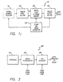
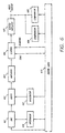
- Fig. 1c is a block diagram of the signal processing system 100 of the present invention.
- the thermal infrared detector 20 is shown in phantom.
- Each detector has an amplifier (not shown) associated therewith which provides an output signal indicative of a change in thermal energy incident on the detector.
- the amplifier outputs are scanned by a semiconductor circuit bonded to the back of the array.
- the output from the array is provided as a serial data stream.
- the chopping momentarily focuses, then removes, the thermal scene from the detector element, allowing for a comparison of the scene with the average value of the scene.
- the result is a first output from the detector amplifier pair which represents the detection of energy from a focused scene and a second output which is a signal of equal and opposite polarity which represents the output of the detector amplifier resulting from the detector seeing the diffused scene.
- the signal processing circuit 100 of Fig. 1c receives these signals from the array 20 and corrects each pixel for sensitivity and offset. Then it offsets and scales the video signal to match the dynamic range of an analog-to-digital converter which converts the video signal to digital form.
- the signal processing circuit 100 includes an analog input section 200, a digital logic circuit 300, a timing circuit 320 and an analog output section 400.
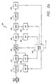
- Fig. 2a is a block diagram of the analog input section 200.
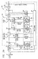
- Fig. 2b is a simplified block diagram of the analog input section and the digital signal processing section 300.
- Serial video signals are multiplexed in from the infrared detector array 20.
- the video signals consist of the two fields of alternating polarity separated by inactive intervals and offset by a DC level.
- This signal is passed through a buffer amplifier 210 and applied to a first adder circuit 212.
- the adder 212 has three inputs: the video signal, an individual pixel offset signal from a first digital-to-analog converter (DAC) 220, and a feedback signal from a first integrator circuit 230.
- DAC digital-to-analog converter
- a uniform cold reference pattern is used to illuminate the array while the outputs are scanned into the field memory 308 of a digital logic circuit 300.
- the inventive digital logic circuit 300 is implemented with a field programmable gate array with firmware stored in a programmable read-only memory (PROM).
- PROM programmable read-only memory
- the invention may be implemented in software in a microprocessor or implemented in hard-wired logic circuits without departing from the scope of the present invention.
- the output of each detector should be zero.
- offset correction signals for the nonzero detector outputs are stored in digital form in a detector coarse DC offset correction memory 302 in the digital logic circuit 300. These signals are used for offset correction of the instantaneous signals output by each detector via a DAC 220 and an adder 212.
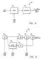
- Fig. 3 is a block diagram of an illustrative implementation the DAC 220.
- a source of reference potential 222 provides a reference signal to a digital potentiometer 224. Since the range of offset correction required varies from detector to detector, the range of the digital-to-analog converter 226 is matched to each detector by the digital potentiometer 224, whereupon, the digital-to-analog converter 226 converts the stored offset signals to an analog output signal for input to the adder 212.
- the integrator 230 averages two successive fields and drives the sum to zero to eliminate the average offsets.
- the first integrator 230 cancels the DC offset of the input signal and performs a function similar to AC coupling with a long time constant. That is, the average value of the active period is set to zero by integrating the video and feeding the result back into the first adder circuit 212.
- Fig. 4 is a block diagram of an illustrative implementation of the first integrator circuit 230.
- the switch 232 receives a blanking signal from a timing circuit 320.
- the RS 170 display controller timing circuit 320 provides timing for the system suitable for the RS 170 video format.
- the blanking signal serves to disable the integrator 234 during inactive periods in the video signal.
- the output of the adder 212 is input to a unity gain inversion circuit or polarity switch 240 which operates under control of the RS 170 timing circuit 320.
- the polarity switch 240 is implemented with an analog multiplier/inverter.
- the input/output waveform of the polarity switch 240 is shown in Figs. 4(a) - 4(b).
- a significant feature of the present invention derives from the inversion of alternating fields of the output of each detector by the unity gain inversion circuit 240. This facilitates field to field subtraction which effectively cancels DC offset in each field while preserving the AC signal for subsequent processing.
- Fig. 4(a) is a waveform illustrating the output of a typical pyroelectric detector.
- Fig. 4(b) is a waveform illustrating a the waveform of Fig. 4(a) after field-to-field gain inversion in accordance with the present teachings.
- Fig. 4(c) illustrates a previous field of output from a pyroelectric detector.
- Fig. 4(d) is a waveform illustrating the output after a summation of the waveforms shown in Figs. 4(b) and 4(c).
- the chopper 19 chops the scene at the field rate so that there is a detector output every field. See Fig. 4(a).
- a second step in the calibration process involves the illumination of the array 20 with a uniform warm reference pattern.
- the outputs of the detectors should be equal.
- the equal and nonequal outputs are digitized and stored in a gain correction memory 304 in the digital logic circuit 300 and used for sensitivity correction via a multiplier 250 and a second DAC circuit 260.
- Fig. 5 is a block diagram of an illustrative implementation of the DAC circuit 260.
- the integrator 262 integrates pulses from the digital logic circuit 300 to create a voltage level proportional to the desired video gain. This controls the global gain applied to the detector with the weakest signal output. This gain factor is reduced to a minimum value for the detector with the strongest output in sensitivity calibration.
- the range of gain control is set by a digital potentiometer 266.
- the integrator 262 and the potentiometer 266 feed a subtractor circuit 264 which in turn provides an input signal to a multiplying D/A (digital-to-analog) converter 265 which sets intermediate levels.
- D/A digital-to-analog
- two feedback loops are used to control the dynamic range of the signal going into the A/D (analog-to-digital) converter 294.
- the output of the A/D converter is fed to a field-to-field automatic global gain and level control circuit 306 in the digital logic circuit 300.
- the field-to-field automatic global gain and level control circuit 306 compares the digitized signal to upper and lower threshold values. If the digital value is above the upper threshold, a high level is output to an offset integrator 280. If the value is below the lower threshold, a low level is sent to the integrator 280. Levels between the thresholds tri-state the output to the integrator resulting in no signal from the digital logic circuit 300.
- This output is also tri-stated during inactive video periods.
- the integrator 280 is referenced to a voltage midway between the two logic levels. The result is that equal numbers of pixels will fall above the upper threshold and below the lower threshold. This provides automatic global level control across the array 20.
- Automatic gain control may be effected in accordance with any one of a number of schemes are well known in the art.
- automatic gain control is provided by generating a high level when the signal is outside the thresholds, a low level when it is within the thresholds, and tri-state when the video is inactive. This is fed to the integrator 262 of Fig. 5 and compared to a reference that is a fraction of the logic level (10% for example). The result is that most of the pixels (90%) will fall between the thresholds and a few pixels (10%) will be above or below the thresholds.
- the digital signals from the analog input section 200 are processed by digital logic circuit 300 and stored in its frame memory.
- the digital output from the digital logic 300 is converted to standard video format (typically RS 170) by an analog output section 400.
- Fig. 6 is a block diagram of an illustrative implementation of the analog output section 400.
- the video signal comes from the digital logic section 300 as successive pixel values. These digital signals are converted to analog form by a DAC 401. The scale factor of these signals is varied by using the output of an integrator 406 as the reference voltage for the DAC 401.
- a second integrator 407 is used to supply an offset voltage which is added to the DAC output in an adder stage 402.
- the output of the adder is then amplified in an amplifier stage 403 to the final output level desired.
- the video signal is then combined with sync and blanking pulses from the digital logic using a clipper circuit 404.
- the clipper circuit 404 is arranged such that the most negative signal passes to its cutput.
- the sync signal is adjusted such that its negative excursion is below the blanking and video signals and its positive excursion is above the video signal range.
- the blanking signal is adjusted such that its negative level is below the video range but above the negative sync level and its positive level is above the video signal range.
- the sync signal is negative, the output is at the sync level regardless of the blanking and video signal levels.
- the sync signal is positive and the blanking level is negative, the output is at the blanking level regardless of the video level.
- both the sync and blanking signals are positive, the output follows the video signal.
- a buffer amplifier 405 provides the output current necessary to drive the load (typically 75 ohms) placed on the circuit. Feedback may be applied around the amplifier clipper and buffer stages to control their overall gain.
- the comparators 408 and 409 are used to detect when the output exceeds the middle of video range (408) or falls outside two thresholds set near the limits of the video range 409.
- the automatic level control operates by using the digital logic to gate the output of the midpoint comparator 408 with the blanking pulse.
- the output of the digital logic is open circuited (tri-state) during the blanking periods. It is low when the video is below the midpoint value and high if the video is above the midpoint value.
- This signal is integrated by an integrator 407 which is referenced to a voltage midway between the high and low logic levels. The output of the integrator controls the offset added to the video signal. An equilibrium condition is established where half of the pixels are above midscale and half are below.
- the other comparator 408 is a window comparator with limits set near the limits of the video range (typically at 10% and 90% of the video range).
- the automatic gain control operates by using digital logic to gate the window comparator with the blanking pulse.
- the output of the digital logic is open circuited (tri-state) during the blanking periods. It is low when the video signal is within the window and high when the video signal is outside the window.
- This signal is integrated by an integrator 406 which is referenced to a voltage that is a fraction of the digital logic voltage (typically 5%).
- the output of the integrator varies the reference voltage of the DAC 401. This forms a feedback loop that reaches an equilibrium condition when 95% of the pixels fall between the 10% and 90% levels of the video range.
- the problems with uncooled detectors are overcome by use of a fast reflective optical system in combination with an uncooled detector.
- the fast reflective optical system provides a high thermal flux to the uncooled detector, thereby compensating for the low sensitivity of the thermal detector.
- Reflective optical systems can be manufactured inexpensively from plastic or aluminum and reduce the need for expensive infrared materials (e.g., germanium) commonly used in military systems.
- the combination of the fast reflective optics and uncooled detector provides a truly low cost thermal camera for night vision.
- the present invention has been described herein with reference to a particular embodiment for a particular application. Those having ordinary skill in the art and access to the present teachings will recognize additional modifications applications and embodiments within the scope thereof.
- the invention is not limited to the use of detectors in the array implemented with barium-strontium-titanate. Other optical arrangements and other detector materials may be used without departing from the scope of the present teachings.
- the uncooled detector may be implemented with a silicon microbolometer such as that disclosed and claimed in U. S. Patent No. 5300915 assigned to Honeywell.
Landscapes
- Physics & Mathematics (AREA)
- Engineering & Computer Science (AREA)
- Multimedia (AREA)
- Signal Processing (AREA)
- General Physics & Mathematics (AREA)
- Optics & Photonics (AREA)
- Toxicology (AREA)
- Health & Medical Sciences (AREA)
- Theoretical Computer Science (AREA)
- Computing Systems (AREA)
- Electromagnetism (AREA)
- Photometry And Measurement Of Optical Pulse Characteristics (AREA)
- Transforming Light Signals Into Electric Signals (AREA)
- Aiming, Guidance, Guns With A Light Source, Armor, Camouflage, And Targets (AREA)
Description
- The present invention relates to imaging systems. More specifically, the present invention relates to night vision systems which sense thermal radiation emitted from an object of interest.
- Night vision systems are well known in the art, Night vision systems typically include a cryogenically cooled linear detector array with an associated cryogenic subsystem, a scanning subsystem which moves a two-dimensional field across the linear array and a refractive optical subsystem which focuses energy onto the detector. The cryogenic coolers typically use liquid cryogenic gases, closed cycle cooler systems or a 3 - 6 stage thermal cooler to operate in typical ambient environments. The detectors in the array sense the emitted heat of the object of interest.
- While these systems have been used extensively for military applications, the high cost of the scanning, cooling and optical systems associated therewith has heretofore limited the applicability of same for numerous other applications.
- Uncooled detectors are inherently low cost since they operate at room temperature and, therefore, do not require expensive and unreliable cryogenic coolers. However, uncooled detectors are not as sensitive as cryogenically cooled detectors. Previous uncooled detectors operating at room temperatures cannot produce clear images of thermal scenes.
- Pyroelectric Imaging by B.M. Kulwicki et al pages 1-10, PROCEEDINGS of the 1992 IEEE International Symposium on Ferroelectrics, 30 Aug to 2nd September 1992, New York, USA discloses a night vision camera utilising an array of uncooled detectors, each detector providing an electrical output signal when illuminated with infra-red energy, a chopper disk, and an electric circuit for processing the output of the array.
- Easily Fabricated wide angle telescope by R.C. Owen, Proceedings of the SPIE International Lens Conference, Vol. 1354, 1990, Bellingham, Washington, USA, pages 430 and 431, discloses an optically fast, compact reflective optical arrangement having a fold mirror located at the systems aperture.
- Accordingly, there has been a need in the art for a low cost night vision system. In particular, there is a need in the art for a low cost night vision system which provides clear images of thermal scenes provided by uncooled detectors.
- The need in the art is addressed by the present invention which provides a night vision camera comprising:
- an array of uncooled detectors, each detector providing an electrical output signal when illuminated with infrared energy;
- a chopper disk; and
- signal processing means for processing an electrical output signal from the array, characterized by further comprising:
- a housing having an upper portion, a lower portion and a subhousing
disposed therebetween, said subhousing having upper and lower parts, said lower
part comprising a cap, and said upper portion having an aperture therethrough:
- a window disposed on the housing at the aperture, the window being transmissive to infrared energy;
- a reflective optical arrangement disposed within the subhousing for focusing a flux of energy of such a quantity as is adapted to compensate for the low sensitivity of said detectors from the aperture onto the array, the optical arrangement including:
- a primary mirror mounted in the upper part of the subhousing and having an aspheric surface and a negative power for reflecting energy from the aperture,
- a secondary mirror mounted on an inner surface of said cap and having an aspheric surface and a positive power for reflecting energy from the primary mirror,
- a fold mirror for reflecting energy from the secondary mirror, and
- a tertiary mirror mounted on an inner surface of said cap and having an
aspheric surface and a positive power for focusing and redirecting energy from the
fold mirror to the array:
- means disposed within said housing for actuating said chopper disk;
- the array is disposed within the housing;
- the chopper disk is disposed within the housing in optical alignment and between the tertiary mirror and the array; and
- the signal processing means is disposed within the housing.
-
- Thus, the problems with uncooled detectors are overcome by use of a fast reflective optical system in combination with an uncooled detector. The fast reflective optical system provides a large thermal flux to the uncooled detector, partially compensating for the lower sensitivity of the thermal detector. Reflective optical systems can be manufactured inexpensively from plastic or aluminum and reduce the need for expensive infrared materials (e.g., germanium and silicon) commonly used in military systems. The combination of the fast reflective optics and uncooled detector provides a truly low cost thermal camera for night vision.
-
- Fig. 1a is a perspective view of an illustrative embodiment of the inventive camera in disassembled relation.
- Fig. 1b is a side view illustrative of the compact optical arrangement of the inventive camera.
- Fig. 1c is a block diagram of the signal processing system of the present invention.
- Fig. 2a is a block diagram of the analog input section of the signal processing system of the present invention.
- Fig. 2b is a simplified block diagram of the analog input section and the digital signal processing section.
- Fig. 3 is a block diagram of an illustrative implementation of a first digital-to-analog converter of the analog section of the signal processing system of the present invention.
- Fig. 4 is a block diagram of an illustrative implementation of a first integrator circuit of the analog section of the signal processing system of the present invention.
- Fig. 4(a) is a waveform illustrating the output of a typical pyroelectric detector.
- Fig. 4(b) is a waveform illustrating a the waveform of Fig. 4(a) after field-to-field gain inversion in accordance with the present teachings.
- Fig. 4(c) illustrates a previous field of output from a pyroelectric detector.
- Fig. 4(d) is a waveform illustrating the output after a summation of the waveforms shown in Figs. 4(b) and 4(c).
- Fig. 5 is a block diagram of an illustrative implementation of a second digital-to-analog converter of the analog section of the signal processing system of the present invention.
- Fig. 6 is a block diagram of an illustrative implementation of the analog output section of the signal processing system of the present invention.
-
- Illustrative embodiments and exemplary applications will now be described with reference to the accompanying drawings to disclose the advantageous teachings of the present invention.
- While the present invention is described herein with reference to illustrative embodiments for particular applications, it should be understood that the invention is not limited thereto. Those having ordinary skill in the art and access to the teachings provided herein will recognize additional modifications, applications, and embodiments within the scope thereof and additional fields in which the present invention would be of significant utility.
- Fig. 1a is a perspective view of an illustrative embodiment of the
inventive camera 1 in disassembled relation. Thecamera 1 includes a housing 2 having anupper portion 3 and alower portion 4. Theupper portion 3 has arectangular aperture 5 therethrough into which aninfrared transmitting window 6 is fitted. Theinfrared transmitting window 6 protects the camera from contaminants. In the preferred embodiment, theinfrared window 6 is constructed in accordance with the teachings of U. S. Patent No. 5,575,959 filed April 22 1994. - A seal 7 is interposed between the upper part of the
housing 3 and the lower part ofhousing 4. The subhousing, consisting of upper and lower parts 8 and 9, supports a compact reflectiveoptical arrangement 10. - Fig. 1b is a side view illustrative of the compact reflective optical arrangement of the inventive camera. The compact reflective optical arrangement is disclosed and claimed in U. S. Patent No. 5,331,470.
As disclosed therein, thearrangement 10 includes aprimary mirror 12, asecondary mirror 14, afold mirror 16, and atertiary mirror 18. The mirrors 12 - 18 (even numbers only) focus energy received through thewindow 6 onto a two-dimensionalfocal plane array 20 of uncooled detector elements. Thus, thecamera 1 stares. Theprimary mirror 12 has anaxis 22 defining the system optical axis. Theprimary mirror 12 is a negative power mirror having a surface which is higher order aspheric. Theprimary mirror 12 is mounted in the subhousing upper part 8. - The
secondary mirror 14 is a positive power mirror and has a surface which is a higher order aspheric. - The
fold mirror 16 is mounted in the subhousing 8 and is optically interposed between thesecondary mirror 14 and thetertiary mirror 18. Thefold mirror 16 is a nonpowered mirror having a nonplanar, preferably higher order aspheric surface. - The
tertiary mirror 18 is a positive power mirror, the surface of which is also a higher order aspheric. - The power of the two positive
powered mirrors primary mirror 12 to provide a zero Petzval curvature or a flat field condition. - The primary and
secondary mirrors mirrors virtual entrance pupil 24 located behind theprimary mirror 12 to areal aperture stop 26. At theaperture stop 26, thefold mirror 16 is positioned to receive the beam from thesecondary mirror 14 and reflect the beam to thetertiary mirror 18. The secondary and tertiary mirrors are disposed on the inner surface of a cap 9. Thetertiary mirror 18 focuses and directs the beam to thedetector array 20 via achopper disk 19. - The
arrangement 10 is from the WALRUS family, since it is a non-relayed three-mirror form with a mirror power distribution of negative, positive, positive used on-axis in aperture and off-axis in field. By locating thefold mirror 16 between thesecondary mirror 14 and thetertiary mirror 18, the optical path is folded back with thesecondary mirror 14 andtertiary mirror 18 adjacent to one another. The length of thearrangement 10 is reduced and the packaging of the optics for the application is considerably improved. Also, by locating thesystem aperture stop 26 at thefold mirror 16, and applying a higher order aspheric surface departure to thefold mirror 16, the spherical aberration of thearrangement 10 is easily corrected, even for very fast optical speeds. The three power mirrors 12, 14 and 18 of the telescope together with thefold mirror 16 form a compact optical system which provides a wide two-dimensional field of view and a very fast optical speed. Fields of view exceeding 20° by 40° can be achieved simultaneously with optical speeds as fast as F/1.0. - The high optical speeds afforded by the present invention are made possible by the use of a large aperture in both the vertical and horizontal planes. In the illustrative embodiment, the field of view is at least 13.5° vertical by 27° horizontal. Since the aperture growth in the vertical plane must be accompanied by an increase in the field of view offset to avoid interference, greater aperture growth can be achieved in the horizontal plane.
- The folding of the optical train between the secondary and
tertiary mirrors system aperture stop 26 provides for a compact arrangement. Also, thefold mirror 16 includes higher order aspheric coefficients which correct the spherical aberration. Further, the optical speed of thearrangement 10 is increased by the use of a large, non-circular aperture and by increasing the offset of the field of view to accommodate the larger aperture. - For higher magnification applications, an alternative reflective triplet design form is preferred such as described in U. S. Patent No. 4,240,707 entitled ALL-REFLECTIVE THREE ELEMENT OBJECTIVE, issued December 23, 1980 to Wetherell et al., An alternative high speed refractive optical design form may also be used for further reduction in optical compactness.
- In the illustrative embodiment, the
focal plane array 20 is fabricated with a plurality of high-performance pyroelectric devices such as the uncooled detectors made of barium-strontium-titanate (BST) manufactured and sold by Texas Instruments. This detector converts infrared energy into an electrical signal without the aid of an expensive cryogenic cooler subsystem that is typically inherent in conventional high-performance night vision imaging systems. - The characteristics of the detectors utilized in the illustrative embodiment are shown in Table I below:
Parameter Value or Requirement Comment Detector resolution Horizontal pixels 328 Vertical pixels 164 NETD(°C) ≤0.1 Average detector NET Modulation transfer function Static square wave response at Nyquist frequency converted to MTF Axial ≥0.2 Best-phase the spread function at video output Off-axis ≥0.15 Area excluding central 20 percent of field of view - A temperature controller (not shown) may be used to maintain the array at room temperature. The temperature controller might include a thermoelectric element thermally coupled to the detector array, a temperature transducer, a voltage reference, and an error amplifier. These form a feedback loop which regulates the detector temperature. The thermoelectric element would be used to either heat or cool the detector array depending on the ambient temperature.
- The uncooled detectors of the illustrative embodiment are most sensitive to thermal contrasts modulated at a predetermined range of frequencies. This modulation of the scene, called "chopping" is accomplished by a rotating optical element phased to provide a thermal differential to each element in the array during each revolution. The chopping momentarily focuses, then removes, the thermal scene from the detector element, allowing for a comparison of the scene with the known reference of the
chopper disk 19. Accordingly in the illustrative embodiment, amechanical chopper 30 is used to modulate the energy incident on thedetector array 20. - Returning to Fig. 1a, the
chopper 30 includes thedisk 19 and amotor 32. The chopper facilitates the sequential readout of thearray 20 and aids in the establishment of a DC reference level for thearray 20 which is representative of the average DC level of the scene. The chopper operates at a 30 hertz rate. Thedisk 19 is fabricated from optical-grade silicon. See U. S. Patent No. 4,227,210 entitled RADIATION SHUTTERS, issued October 7, 1980 to R. D. Nixon. See also GB 2,240,000 entitled THERMAL-RADIATION DETECTION SYSTEMS AND OPTICAL CHOPPERS, published July 17, 1991 in the name of A. A. Turnbull.) A suitable alternative detector, for example, would be a silicon microbolometer detector fabricated by Hughes Aircraft Company; Honeywell, Inc.; and Loral. - A
signal processing system 100 processes the output of thearray 20 for display on any standard video screen. In addition, irregularities in the outputs of the detectors across thearray 20 in response to a test pattern are corrected by thesystem 100. Thesystem 100 provides power to thechopper motor 32 and is itself powered by apower supply 42. Thepower supply 42 is connected to external circuitry such as a display (not shown) by acable 46 through aport 48. Input power is converted into the required secondary voltages for use within thecamera 1. - Fig. 1c is a block diagram of the
signal processing system 100 of the present invention. The thermalinfrared detector 20 is shown in phantom. Each detector has an amplifier (not shown) associated therewith which provides an output signal indicative of a change in thermal energy incident on the detector. The amplifier outputs are scanned by a semiconductor circuit bonded to the back of the array. The output from the array is provided as a serial data stream. - As mentioned above, the chopping momentarily focuses, then removes, the thermal scene from the detector element, allowing for a comparison of the scene with the average value of the scene. The result is a first output from the detector amplifier pair which represents the detection of energy from a focused scene and a second output which is a signal of equal and opposite polarity which represents the output of the detector amplifier resulting from the detector seeing the diffused scene. These two fields constitute a single frame.
- The
signal processing circuit 100 of Fig. 1c receives these signals from thearray 20 and corrects each pixel for sensitivity and offset. Then it offsets and scales the video signal to match the dynamic range of an analog-to-digital converter which converts the video signal to digital form. Thesignal processing circuit 100 includes ananalog input section 200, adigital logic circuit 300, atiming circuit 320 and ananalog output section 400. - Fig. 2a is a block diagram of the
analog input section 200. Fig. 2b is a simplified block diagram of the analog input section and the digitalsignal processing section 300. Serial video signals are multiplexed in from theinfrared detector array 20. As mentioned above, the video signals consist of the two fields of alternating polarity separated by inactive intervals and offset by a DC level. This signal is passed through abuffer amplifier 210 and applied to afirst adder circuit 212. Theadder 212 has three inputs: the video signal, an individual pixel offset signal from a first digital-to-analog converter (DAC) 220, and a feedback signal from afirst integrator circuit 230. - In accordance with the present teachings, in a calibration mode, a uniform cold reference pattern is used to illuminate the array while the outputs are scanned into the
field memory 308 of adigital logic circuit 300. In the preferred embodiment, the inventivedigital logic circuit 300 is implemented with a field programmable gate array with firmware stored in a programmable read-only memory (PROM). However, those skilled in the art will appreciate that the invention may be implemented in software in a microprocessor or implemented in hard-wired logic circuits without departing from the scope of the present invention. The output of each detector should be zero. As discussed more fully below, offset correction signals for the nonzero detector outputs are stored in digital form in a detector coarse DC offsetcorrection memory 302 in thedigital logic circuit 300. These signals are used for offset correction of the instantaneous signals output by each detector via aDAC 220 and anadder 212. - Fig. 3 is a block diagram of an illustrative implementation the
DAC 220. A source ofreference potential 222 provides a reference signal to adigital potentiometer 224. Since the range of offset correction required varies from detector to detector, the range of the digital-to-analog converter 226 is matched to each detector by thedigital potentiometer 224, whereupon, the digital-to-analog converter 226 converts the stored offset signals to an analog output signal for input to theadder 212. - The
integrator 230 averages two successive fields and drives the sum to zero to eliminate the average offsets. Thefirst integrator 230 cancels the DC offset of the input signal and performs a function similar to AC coupling with a long time constant. That is, the average value of the active period is set to zero by integrating the video and feeding the result back into thefirst adder circuit 212. - Fig. 4 is a block diagram of an illustrative implementation of the
first integrator circuit 230. Theswitch 232 receives a blanking signal from atiming circuit 320. The RS 170 displaycontroller timing circuit 320 provides timing for the system suitable for the RS 170 video format. The blanking signal serves to disable theintegrator 234 during inactive periods in the video signal. - Returning to Fig. 2b, the output of the
adder 212 is input to a unity gain inversion circuit orpolarity switch 240 which operates under control of the RS 170timing circuit 320. Thepolarity switch 240 is implemented with an analog multiplier/inverter. The input/output waveform of thepolarity switch 240 is shown in Figs. 4(a) - 4(b). As discussed more fully below, a significant feature of the present invention derives from the inversion of alternating fields of the output of each detector by the unitygain inversion circuit 240. This facilitates field to field subtraction which effectively cancels DC offset in each field while preserving the AC signal for subsequent processing. - Fig. 4(a) is a waveform illustrating the output of a typical pyroelectric detector. Fig. 4(b) is a waveform illustrating a the waveform of Fig. 4(a) after field-to-field gain inversion in accordance with the present teachings. Fig. 4(c) illustrates a previous field of output from a pyroelectric detector. Fig. 4(d) is a waveform illustrating the output after a summation of the waveforms shown in Figs. 4(b) and 4(c).
- As mentioned above, the
chopper 19 chops the scene at the field rate so that there is a detector output every field. See Fig. 4(a). Thepolarity switch 240 effects field-to-field gain inversion in such a way that for the even fields (n = 0, 2, 4, 6, ...), the resulting output equals (1) times the detector output and for the odd fields (n = 1, 3, 5, ...), the resulting output equals (-1) times the detector output. See Fig. 4(b). Then the inverted signal is digitized by the analog-to-digital converter 294. Alternating fields are stored in afield memory 308. Data from a previous field (field n - 1) (Fig. 4(c)) is retrieved from thefield memory 308 and summed with the current field (field n) to cancel the DC bias in each field (Fig. 4(d)). As shown in Fig. 4(d), after summing fields n - 1 and n together in theadder 310, the detector DC bias is canceled, but the resulting detector scene signal is doubled. Hence, a divide by twocircuit 312 is used to scale the detector scene signal back to its correct signal amplitude. - A second step in the calibration process involves the illumination of the
array 20 with a uniform warm reference pattern. The outputs of the detectors should be equal. The equal and nonequal outputs are digitized and stored in again correction memory 304 in thedigital logic circuit 300 and used for sensitivity correction via amultiplier 250 and asecond DAC circuit 260. - Fig. 5 is a block diagram of an illustrative implementation of the
DAC circuit 260. Theintegrator 262 integrates pulses from thedigital logic circuit 300 to create a voltage level proportional to the desired video gain. This controls the global gain applied to the detector with the weakest signal output. This gain factor is reduced to a minimum value for the detector with the strongest output in sensitivity calibration. The range of gain control is set by adigital potentiometer 266. Theintegrator 262 and thepotentiometer 266 feed asubtractor circuit 264 which in turn provides an input signal to a multiplying D/A (digital-to-analog)converter 265 which sets intermediate levels. As the range of the D/A converter is reduced, a complementary DC level is added to the output by aninverter 268 and asubtractor 267 to keep the full scale output of themultiplier 250 constant. - Returning to Fig. 2b, in addition to a
limiter 290, two feedback loops are used to control the dynamic range of the signal going into the A/D (analog-to-digital)converter 294. The output of the A/D converter is fed to a field-to-field automatic global gain andlevel control circuit 306 in thedigital logic circuit 300. The field-to-field automatic global gain andlevel control circuit 306 compares the digitized signal to upper and lower threshold values. If the digital value is above the upper threshold, a high level is output to an offsetintegrator 280. If the value is below the lower threshold, a low level is sent to theintegrator 280. Levels between the thresholds tri-state the output to the integrator resulting in no signal from thedigital logic circuit 300. This output is also tri-stated during inactive video periods. Theintegrator 280 is referenced to a voltage midway between the two logic levels. The result is that equal numbers of pixels will fall above the upper threshold and below the lower threshold. This provides automatic global level control across thearray 20. - Automatic gain control may be effected in accordance with any one of a number of schemes are well known in the art. In the preferred embodiment, automatic gain control is provided by generating a high level when the signal is outside the thresholds, a low level when it is within the thresholds, and tri-state when the video is inactive. This is fed to the
integrator 262 of Fig. 5 and compared to a reference that is a fraction of the logic level (10% for example). The result is that most of the pixels (90%) will fall between the thresholds and a few pixels (10%) will be above or below the thresholds. - Thus, as depicted in Fig. 1c, the digital signals from the
analog input section 200 are processed bydigital logic circuit 300 and stored in its frame memory. The digital output from thedigital logic 300 is converted to standard video format (typically RS 170) by ananalog output section 400. - Fig. 6 is a block diagram of an illustrative implementation of the
analog output section 400. The video signal comes from thedigital logic section 300 as successive pixel values. These digital signals are converted to analog form by aDAC 401. The scale factor of these signals is varied by using the output of anintegrator 406 as the reference voltage for theDAC 401. Asecond integrator 407 is used to supply an offset voltage which is added to the DAC output in anadder stage 402. The output of the adder is then amplified in anamplifier stage 403 to the final output level desired. The video signal is then combined with sync and blanking pulses from the digital logic using aclipper circuit 404. Theclipper circuit 404 is arranged such that the most negative signal passes to its cutput. The sync signal is adjusted such that its negative excursion is below the blanking and video signals and its positive excursion is above the video signal range. The blanking signal is adjusted such that its negative level is below the video range but above the negative sync level and its positive level is above the video signal range. When the sync signal is negative, the output is at the sync level regardless of the blanking and video signal levels. When the sync signal is positive and the blanking level is negative, the output is at the blanking level regardless of the video level. When both the sync and blanking signals are positive, the output follows the video signal. Abuffer amplifier 405 provides the output current necessary to drive the load (typically 75 ohms) placed on the circuit. Feedback may be applied around the amplifier clipper and buffer stages to control their overall gain. - The
comparators video range 409. - The automatic level control operates by using the digital logic to gate the output of the
midpoint comparator 408 with the blanking pulse. The output of the digital logic is open circuited (tri-state) during the blanking periods. It is low when the video is below the midpoint value and high if the video is above the midpoint value. This signal is integrated by anintegrator 407 which is referenced to a voltage midway between the high and low logic levels. The output of the integrator controls the offset added to the video signal. An equilibrium condition is established where half of the pixels are above midscale and half are below. - The
other comparator 408 is a window comparator with limits set near the limits of the video range (typically at 10% and 90% of the video range). The automatic gain control operates by using digital logic to gate the window comparator with the blanking pulse. The output of the digital logic is open circuited (tri-state) during the blanking periods. It is low when the video signal is within the window and high when the video signal is outside the window. This signal is integrated by anintegrator 406 which is referenced to a voltage that is a fraction of the digital logic voltage (typically 5%). The output of the integrator varies the reference voltage of theDAC 401. This forms a feedback loop that reaches an equilibrium condition when 95% of the pixels fall between the 10% and 90% levels of the video range. - While these circuits may be implemented in a manner well within the ability of one of ordinary skill in the art, in the preferred embodiment, the circuits disclosed and claimed in U. S. Patent Nos. 5591973 and 5526035 would be used for the illustrative application.
- Thus, in accordance with the present teachings, the problems with uncooled detectors are overcome by use of a fast reflective optical system in combination with an uncooled detector. The fast reflective optical system provides a high thermal flux to the uncooled detector, thereby compensating for the low sensitivity of the thermal detector. Reflective optical systems can be manufactured inexpensively from plastic or aluminum and reduce the need for expensive infrared materials (e.g., germanium) commonly used in military systems. The combination of the fast reflective optics and uncooled detector provides a truly low cost thermal camera for night vision.
- The present invention has been described herein with reference to a particular embodiment for a particular application. Those having ordinary skill in the art and access to the present teachings will recognize additional modifications applications and embodiments within the scope thereof. For example, the invention is not limited to the use of detectors in the array implemented with barium-strontium-titanate. Other optical arrangements and other detector materials may be used without departing from the scope of the present teachings. For example, in lieu of a pyroelectric detector, the uncooled detector may be implemented with a silicon microbolometer such as that disclosed and claimed in U. S. Patent No. 5300915 assigned to Honeywell.
- It is therefore intended by the appended claims to cover any and all such applications, modifications and embodiments within the scope of the present invention.
Claims (6)
- A night vision camera (1) comprising:characterized by further comprising:an array (20) of uncooled detectors, each detector providing an electrical output signal when illuminated with infrared energy;a chopper disk (19); andsignal processing means (100) for processing an electrical output signal from the array,wherein:a housing (2) having an upper portion, a lower portion (4) and a subhousing (8,9) disposed therebetween, said subhousing having upper and lower parts (8,9), said lower part (8) comprising a cap (9), and said upper portion having an aperture therethrough (5):a window (6) disposed on the housing at the aperture (5), the window being transmissive to infrared energy;a reflective optical arrangement (10) disposed within the subhousing for focusing a flux of energy of such a quantity wich is adapted to compensate for the low sensitivity of said detectors from the aperture onto the array, the optical arrangement including:a primary mirror (12) mounted in the upper part of the subhousing and having an aspheric surface and a negative power for reflecting energy from the aperture,a secondary mirror (14) mounted on an inner surface of said cap and having an aspheric surface and a positive power for reflecting energy from the primary mirror,a fold mirror (16) for reflecting energy from the secondary mirror, anda tertiary mirror (18) mounted on an inner surface of said cap and having an aspheric surface and a positive power for focusing and redirecting energy from the fold mirror to the array:means (32) disposed within said housing for actuating said chopper disk;the array (20) is disposed within the housing (2);the chopper disk (19) is disposed within the housing in optical alignment and between the tertiary mirror (18) and the array (20); andthe signal processing means (100) is disposed within the housing.
- The night vision camera of claim 1 wherein the power of the secondary (14) and tertiary (18) mirrors is balanced by the negative power of the primary mirror (12) to provide a zero Petzval curvature or flat field condition.
- The night vision camera of either of claims 1 or 2 wherein the primary (12) and secondary (14) mirrors form a non-reimaging afocal telescope of the Galilean type at an afocal magnification of approximately 2x.
- The night vision camera of any preceding claim wherein the primary (12) and secondary (14) mirrors relay a virtual entrance pupil (24) located behind the primary mirror (12) to a real aperture stop (26).
- The night vision camera of claim 4 wherein the fold mirror (16) is positioned at the aperture stop (26) to receive the energy from the secondary mirror (14) and reflect the energy to the tertiary (18) mirror.
- The night vision camera of claim 1 wherein the reflective optical arrangement (10) is a non-relayed three-mirror arrangement with a mirror power distribution of negative, positive, positive used on-axis in aperture and off-axis in field.
Applications Claiming Priority (2)
| Application Number | Priority Date | Filing Date | Title |
|---|---|---|---|
| US23289394A | 1994-04-12 | 1994-04-12 | |
| US232893 | 1994-04-12 |
Publications (3)
| Publication Number | Publication Date |
|---|---|
| EP0677955A2 EP0677955A2 (en) | 1995-10-18 |
| EP0677955A3 EP0677955A3 (en) | 1997-08-20 |
| EP0677955B1 true EP0677955B1 (en) | 2003-01-02 |
Family
ID=22875025
Family Applications (1)
| Application Number | Title | Priority Date | Filing Date |
|---|---|---|---|
| EP95302393A Expired - Lifetime EP0677955B1 (en) | 1994-04-12 | 1995-04-11 | Low cost night vision camera |
Country Status (5)
| Country | Link |
|---|---|
| US (1) | US5763882A (en) |
| EP (1) | EP0677955B1 (en) |
| JP (1) | JPH0846838A (en) |
| KR (1) | KR0173826B1 (en) |
| DE (1) | DE69529243T2 (en) |
Families Citing this family (37)
| Publication number | Priority date | Publication date | Assignee | Title |
|---|---|---|---|---|
| DE69529243T2 (en) * | 1994-04-12 | 2003-10-16 | Raytheon Co | Inexpensive after viewing device |
| US5619036A (en) * | 1994-04-12 | 1997-04-08 | Hughes Electronics | Low cost night vision camera for vehicles and mounting thereof |
| GB2296147B (en) * | 1994-11-29 | 1999-06-16 | Marconi Gec Ltd | A signal processor |
| US5920066A (en) * | 1996-08-02 | 1999-07-06 | Raytheon Company | Real-time adaptive thermal reference control for night vision systems |
| JP3019010B2 (en) * | 1996-11-13 | 2000-03-13 | 日本電気株式会社 | Imaging device |
| US6322670B2 (en) * | 1996-12-31 | 2001-11-27 | Honeywell International Inc. | Flexible high performance microbolometer detector material fabricated via controlled ion beam sputter deposition process |
| JPH10281864A (en) * | 1997-04-03 | 1998-10-23 | Nikon Corp | Thermal infrared camera |
| WO2000037314A1 (en) | 1998-12-21 | 2000-06-29 | Alliedsignal Inc. | Ir diode based high intensity light |
| US6486473B2 (en) | 2000-03-02 | 2002-11-26 | Mine Safety Applicances Company | Thermal imaging camera |
| SE519864C2 (en) * | 2000-10-26 | 2003-04-15 | Autoliv Dev | Device for improving the night vision of a vehicle such as a car |
| US20030202097A1 (en) | 2000-10-26 | 2003-10-30 | Autoliv Development Ab | Night vision arrangement |
| US6833822B2 (en) * | 2000-12-21 | 2004-12-21 | Raytheon Company | Method and apparatus for generating a visible image with an infrared transmissive window |
| US6491417B1 (en) * | 2001-06-13 | 2002-12-10 | Bendix Commercial Vehicle Systems Llc | Night vision clearance light |
| US7995095B2 (en) | 2001-10-18 | 2011-08-09 | Autoliv Development Ab | Night vision device for a vehicle |
| US7796316B2 (en) | 2001-12-21 | 2010-09-14 | Bodkin Design And Engineering Llc | Micro-optic shutter |
| US8174694B2 (en) * | 2001-12-21 | 2012-05-08 | Bodkin Design And Engineering Llc | Hyperspectral imaging systems |
| US20060072109A1 (en) * | 2004-09-03 | 2006-04-06 | Andrew Bodkin | Hyperspectral imaging systems |
| US7049597B2 (en) * | 2001-12-21 | 2006-05-23 | Andrew Bodkin | Multi-mode optical imager |
| EP1497155B1 (en) | 2002-04-23 | 2006-08-16 | Autoliv Development Ab | A night vision arrangement |
| WO2004011304A1 (en) * | 2002-07-29 | 2004-02-05 | Raytheon Company | System and method for deploying a mirror assembly of a display unit |
| RU2234818C2 (en) * | 2002-07-29 | 2004-08-20 | Федеральное государственное унитарное предприятие "Научно-исследовательский институт промышленного телевидения "Растр" | Day-and-night intrusion-protection television system |
| US6837581B1 (en) | 2002-07-29 | 2005-01-04 | Raytheon Company | System and method for deploying a mirror assembly of a display unit |
| US8483567B2 (en) * | 2004-04-09 | 2013-07-09 | Immediate Response Technologies, Inc | Infrared communication system and method |
| DE102004026993B4 (en) * | 2004-06-03 | 2010-04-01 | Carl Zeiss Jena Gmbh | camera |
| US7411194B1 (en) * | 2005-11-09 | 2008-08-12 | Kollsman, Inc. | Aviation vision apparatus |
| US7767963B1 (en) | 2006-12-08 | 2010-08-03 | Draeger Safety, Inc. | Thermal imaging camera internal damping system |
| US8922783B2 (en) | 2007-04-27 | 2014-12-30 | Bodkin Design And Engineering Llc | Multiband spatial heterodyne spectrometer and associated methods |
| US8154732B2 (en) * | 2007-04-27 | 2012-04-10 | Bodkin Design And Engineering, Llc | Multiband spatial heterodyne spectrometer and associated methods |
| US8555721B2 (en) * | 2007-12-27 | 2013-10-15 | Scott Taillet | Sound measuring device |
| US9209888B2 (en) | 2011-09-27 | 2015-12-08 | Rivada Research, Llc | Method and system for providing explosion proof video and communication relay module |
| US9744384B2 (en) | 2011-11-05 | 2017-08-29 | Rivada Research, Llc | Enhanced display for breathing apparatus masks |
| TWI616680B (en) * | 2016-04-01 | 2018-03-01 | 鴻海精密工業股份有限公司 | Off-axial three-mirror optical system with freeform surfaces |
| EP3527429B1 (en) * | 2018-02-15 | 2021-04-07 | Aptiv Technologies Limited | Module and support structure assembly |
| US10924685B2 (en) | 2018-05-07 | 2021-02-16 | Rubicon Products, LLC | Night vision apparatus |
| US12228724B2 (en) | 2020-07-10 | 2025-02-18 | Goodrich Corporation | Modular reconfigurable optical systems for supporting multiple modalities |
| US11268860B2 (en) | 2020-07-24 | 2022-03-08 | Raytheon Company | Radiometric calibration of detector |
| US11622062B1 (en) | 2021-04-05 | 2023-04-04 | United States Of America As Represented By The Administrator Of Nasa | Ruggedized miniaturized infrared camera system for aerospace environments |
Family Cites Families (25)
| Publication number | Priority date | Publication date | Assignee | Title |
|---|---|---|---|---|
| US3610930A (en) * | 1968-12-31 | 1971-10-05 | Texas Instruments Inc | Independent infrared landing monitor |
| US3617107A (en) * | 1969-07-28 | 1971-11-02 | Bell Telephone Labor Inc | Three-mirror schmidt telescope |
| US3886360A (en) * | 1973-09-04 | 1975-05-27 | Gulf & Western Mfg Co | Infrared intrusion detection apparatus |
| US4142207A (en) * | 1977-12-20 | 1979-02-27 | Texas Instruments Incorporated | Ferroelectric imaging system |
| US4950896A (en) * | 1978-07-18 | 1990-08-21 | The United States Of America As Represented By The Secretary Of The Army | Modified forward looking IR device to include wide angle black hole radiometer |
| US4277804A (en) * | 1978-11-01 | 1981-07-07 | Elburn Robison | System for viewing the area rearwardly of a vehicle |
| US4265510A (en) * | 1979-05-16 | 1981-05-05 | Hughes Aircraft Company | Three mirror anastigmatic optical system |
| JPS56133634A (en) * | 1980-03-25 | 1981-10-19 | Toshiba Corp | Pyroelectric detector |
| JPS61173124A (en) * | 1985-01-28 | 1986-08-04 | Matsushita Electric Ind Co Ltd | Pyroelectric thermal imager |
| US4806761A (en) * | 1985-04-08 | 1989-02-21 | Irvine Sensors Corporation | Thermal imager incorporating electronics module having focal plane sensor mosaic |
| US5001558A (en) * | 1985-06-11 | 1991-03-19 | General Motors Corporation | Night vision system with color video camera |
| US4719350A (en) * | 1986-01-30 | 1988-01-12 | Hughes Aircraft Co. | Radiation imaging enhancement |
| US4733955A (en) * | 1986-04-14 | 1988-03-29 | Hughes Aircraft Company | Reflective optical triplet having a real entrance pupil |
| US4804258A (en) * | 1986-05-05 | 1989-02-14 | Hughes Aircraft Company | Four mirror afocal wide field of view optical system |
| JPS6365328A (en) * | 1986-09-08 | 1988-03-23 | Matsushita Electric Ind Co Ltd | Two-dimensional infrared imaging device |
| JPS63282621A (en) * | 1987-05-14 | 1988-11-18 | Matsushita Electric Ind Co Ltd | One-dimensional infrared image sensing device |
| US5021663B1 (en) * | 1988-08-12 | 1997-07-01 | Texas Instruments Inc | Infrared detector |
| US5114238A (en) * | 1990-06-28 | 1992-05-19 | Lockheed Missiles & Space Company, Inc. | Infrared catadioptric zoom relay telescope |
| US5173801A (en) * | 1991-08-16 | 1992-12-22 | Hughes Aircraft Company | Wide field of view afocal three-mirror anastigmat |
| US5331470A (en) * | 1992-12-11 | 1994-07-19 | Hughes Aircraft Company | Fast folded wide angle large reflective unobscured system |
| GB9317983D0 (en) * | 1993-08-28 | 1993-10-13 | Lucas Ind Plc | A driver assistance system for a vehicle |
| US5379157A (en) * | 1993-12-02 | 1995-01-03 | Hughes Aircraft Company | Compact, folded wide-angle large reflective unobscured optical system |
| DE69529243T2 (en) * | 1994-04-12 | 2003-10-16 | Raytheon Co | Inexpensive after viewing device |
| US5414439A (en) * | 1994-06-09 | 1995-05-09 | Delco Electronics Corporation | Head up display with night vision enhancement |
| US5554847A (en) * | 1994-10-11 | 1996-09-10 | Hughes Aircraft Company | Flexibly connectable high precision thermal and structural focal plane array mount |
-
1995
- 1995-04-11 DE DE69529243T patent/DE69529243T2/en not_active Expired - Fee Related
- 1995-04-11 EP EP95302393A patent/EP0677955B1/en not_active Expired - Lifetime
- 1995-04-12 JP JP7087290A patent/JPH0846838A/en active Pending
- 1995-04-12 KR KR1019950008466A patent/KR0173826B1/en not_active Expired - Fee Related
-
1996
- 1996-11-18 US US08/751,393 patent/US5763882A/en not_active Expired - Fee Related
Also Published As
| Publication number | Publication date |
|---|---|
| KR950029837A (en) | 1995-11-24 |
| JPH0846838A (en) | 1996-02-16 |
| EP0677955A3 (en) | 1997-08-20 |
| EP0677955A2 (en) | 1995-10-18 |
| KR0173826B1 (en) | 1999-03-20 |
| US5763882A (en) | 1998-06-09 |
| DE69529243D1 (en) | 2003-02-06 |
| DE69529243T2 (en) | 2003-10-16 |
Similar Documents
| Publication | Publication Date | Title |
|---|---|---|
| US5763882A (en) | Low cost night vision camera | |
| US5591973A (en) | Signal processor for infrared camera | |
| US4466748A (en) | Thermal imaging apparatus | |
| US6515285B1 (en) | Method and apparatus for compensating a radiation sensor for ambient temperature variations | |
| US7495220B2 (en) | Uncooled infrared sensor | |
| EP0277696B1 (en) | Thermal imager | |
| EP0766112B1 (en) | Panoramic optics assembly having an initial flat reflective element | |
| US5528035A (en) | Digital signal processing system for removing DC bias in the output of pyroelectric and similar detectors | |
| KR19990036107A (en) | Thermal Sensing System with Fast Response Calibrator | |
| JPH07507389A (en) | Infrared image recording device | |
| US5510618A (en) | Second generation FLIR common modules | |
| EP0766113B1 (en) | Aspherical elements for infrared imaging system | |
| EP0216924A1 (en) | Thermal imager incorporating sensor within electronics module | |
| GB2305799A (en) | Thermal imaging system with controlled mean scene reference temperature source | |
| Broekaert et al. | Nonlinearity and nonuniformity corrections for the IRIS family of IRCCD thermal imagers | |
| Kruse et al. | Infrared imager employing a 160x120 pixel uncooled bolometer array | |
| Tanaka et al. | Performance of 320x240 uncooled bolometer-type infrared focal plane arrays | |
| Nichols et al. | Performance characteristics of a submarine panoramic infrared imaging sensor | |
| Akasaka et al. | Short-wavelength infrared subsystem design status of ASTER | |
| Kimball et al. | Dual-band optical system for IR multicolor signal processing | |
| Tomono et al. | Mid-infrared test observation system (MIRTOS) for Subaru | |
| Anderson | TV-compatible forward looking infrared | |
| Balcerak et al. | Advances in infrared sensor technology and systems | |
| McEwen et al. | An uncooled solid state thermal imager | |
| Fujisada | High-sensitive thermal video camera with self-scanned 128 InSb linear array |
Legal Events
| Date | Code | Title | Description |
|---|---|---|---|
| PUAI | Public reference made under article 153(3) epc to a published international application that has entered the european phase |
Free format text: ORIGINAL CODE: 0009012 |
|
| AK | Designated contracting states |
Kind code of ref document: A2 Designated state(s): DE FR GB SE |
|
| PUAL | Search report despatched |
Free format text: ORIGINAL CODE: 0009013 |
|
| AK | Designated contracting states |
Kind code of ref document: A3 Designated state(s): DE FR GB SE |
|
| 17P | Request for examination filed |
Effective date: 19980127 |
|
| RAP1 | Party data changed (applicant data changed or rights of an application transferred) |
Owner name: RAYTHEON COMPANY |
|
| 17Q | First examination report despatched |
Effective date: 20000512 |
|
| GRAG | Despatch of communication of intention to grant |
Free format text: ORIGINAL CODE: EPIDOS AGRA |
|
| GRAG | Despatch of communication of intention to grant |
Free format text: ORIGINAL CODE: EPIDOS AGRA |
|
| GRAH | Despatch of communication of intention to grant a patent |
Free format text: ORIGINAL CODE: EPIDOS IGRA |
|
| GRAH | Despatch of communication of intention to grant a patent |
Free format text: ORIGINAL CODE: EPIDOS IGRA |
|
| GRAA | (expected) grant |
Free format text: ORIGINAL CODE: 0009210 |
|
| AK | Designated contracting states |
Kind code of ref document: B1 Designated state(s): DE FR GB SE |
|
| REG | Reference to a national code |
Ref country code: GB Ref legal event code: FG4D Free format text: 20030102 |
|
| REF | Corresponds to: |
Ref document number: 69529243 Country of ref document: DE Date of ref document: 20030206 Kind code of ref document: P |
|
| REG | Reference to a national code |
Ref country code: SE Ref legal event code: TRGR |
|
| ET | Fr: translation filed | ||
| PLBE | No opposition filed within time limit |
Free format text: ORIGINAL CODE: 0009261 |
|
| STAA | Information on the status of an ep patent application or granted ep patent |
Free format text: STATUS: NO OPPOSITION FILED WITHIN TIME LIMIT |
|
| 26N | No opposition filed |
Effective date: 20031003 |
|
| REG | Reference to a national code |
Ref country code: GB Ref legal event code: 732E |
|
| REG | Reference to a national code |
Ref country code: FR Ref legal event code: TP |
|
| PGFP | Annual fee paid to national office [announced via postgrant information from national office to epo] |
Ref country code: DE Payment date: 20080418 Year of fee payment: 14 |
|
| PGFP | Annual fee paid to national office [announced via postgrant information from national office to epo] |
Ref country code: SE Payment date: 20080414 Year of fee payment: 14 |
|
| PGFP | Annual fee paid to national office [announced via postgrant information from national office to epo] |
Ref country code: FR Payment date: 20080412 Year of fee payment: 14 |
|
| PGFP | Annual fee paid to national office [announced via postgrant information from national office to epo] |
Ref country code: GB Payment date: 20080421 Year of fee payment: 14 |
|
| EUG | Se: european patent has lapsed | ||
| GBPC | Gb: european patent ceased through non-payment of renewal fee |
Effective date: 20090411 |
|
| REG | Reference to a national code |
Ref country code: FR Ref legal event code: ST Effective date: 20091231 |
|
| PG25 | Lapsed in a contracting state [announced via postgrant information from national office to epo] |
Ref country code: DE Free format text: LAPSE BECAUSE OF NON-PAYMENT OF DUE FEES Effective date: 20091103 |
|
| PG25 | Lapsed in a contracting state [announced via postgrant information from national office to epo] |
Ref country code: GB Free format text: LAPSE BECAUSE OF NON-PAYMENT OF DUE FEES Effective date: 20090411 Ref country code: FR Free format text: LAPSE BECAUSE OF NON-PAYMENT OF DUE FEES Effective date: 20091222 |
|
| PG25 | Lapsed in a contracting state [announced via postgrant information from national office to epo] |
Ref country code: SE Free format text: LAPSE BECAUSE OF NON-PAYMENT OF DUE FEES Effective date: 20090412 |