EP0672260B1 - Arrangement for reading information from a track on a record carrier comprising a fast settling read amplifier for magneto-resistive heads - Google Patents
Arrangement for reading information from a track on a record carrier comprising a fast settling read amplifier for magneto-resistive heads Download PDFInfo
- Publication number
- EP0672260B1 EP0672260B1 EP94926362A EP94926362A EP0672260B1 EP 0672260 B1 EP0672260 B1 EP 0672260B1 EP 94926362 A EP94926362 A EP 94926362A EP 94926362 A EP94926362 A EP 94926362A EP 0672260 B1 EP0672260 B1 EP 0672260B1
- Authority
- EP
- European Patent Office
- Prior art keywords
- terminal
- transistor
- main flow
- coupled
- arrangement
- Prior art date
- Legal status (The legal status is an assumption and is not a legal conclusion. Google has not performed a legal analysis and makes no representation as to the accuracy of the status listed.)
- Expired - Lifetime
Links
- 239000003990 capacitor Substances 0.000 claims description 55
- 230000004044 response Effects 0.000 claims description 3
- 230000008901 benefit Effects 0.000 description 5
- 238000010276 construction Methods 0.000 description 5
- 238000007599 discharging Methods 0.000 description 4
- 230000009977 dual effect Effects 0.000 description 4
- 238000000605 extraction Methods 0.000 description 4
- 230000001965 increasing effect Effects 0.000 description 4
- 230000006872 improvement Effects 0.000 description 3
- 238000003546 multiplexed readout Methods 0.000 description 3
- 230000001052 transient effect Effects 0.000 description 3
- 230000003321 amplification Effects 0.000 description 2
- 239000004020 conductor Substances 0.000 description 2
- 238000002347 injection Methods 0.000 description 2
- 239000007924 injection Substances 0.000 description 2
- 238000003199 nucleic acid amplification method Methods 0.000 description 2
- 230000009467 reduction Effects 0.000 description 2
- 230000009897 systematic effect Effects 0.000 description 2
- 230000003213 activating effect Effects 0.000 description 1
- 230000008859 change Effects 0.000 description 1
- 230000008878 coupling Effects 0.000 description 1
- 238000010168 coupling process Methods 0.000 description 1
- 238000005859 coupling reaction Methods 0.000 description 1
- 238000006880 cross-coupling reaction Methods 0.000 description 1
- 230000003247 decreasing effect Effects 0.000 description 1
- 230000001934 delay Effects 0.000 description 1
- 230000001419 dependent effect Effects 0.000 description 1
- 238000010586 diagram Methods 0.000 description 1
- 230000000694 effects Effects 0.000 description 1
- 230000001939 inductive effect Effects 0.000 description 1
- 230000010354 integration Effects 0.000 description 1
- 238000000034 method Methods 0.000 description 1
- 238000004904 shortening Methods 0.000 description 1
- 239000010409 thin film Substances 0.000 description 1
Images






Definitions
- the invention relates to an arrangement for reading out an information signal from a magnetic record carrier, comprising:
- the feedback circuit is a transconductance stage having a low transconductance Gm.
- the maximum output current of such a transconductance stage severely limits the speed of charging and discharging of the capacitor element and gives rise to transients with a duration of hundreds of microseconds. This is too long for fast mass storage devices.
- the transconductance Gm of the transconductance stage is temporarily increased by increasing its bias current. This, however, causes unacceptable errors because of increased offset of the transconductance stage.
- the known arrangement is characterized in that the feedback means comprises:
- the voltage buffer means provide the high currents needed to charge or discharge the capacitor element when the series resistor is short circuited by the switch connected in parallel to the series resistor. Only a passive element, that is a bias current free element, is short circuited and no offset is created by the short circuiting. In this way a very fast settling is possible without loosing the desired accuracy in settling of the read amplifier.
- a first fast settling arrangement is characterized in that the voltage buffer means comprises a first current source and a second current source, a second transistor having a control terminal connected to a second main flow terminal and a third transistor, a first main flow terminal of the second transistor and a first main flow terminal of the third transistor being interconnected and coupled to the first point of constant potential via the first current source, the second main flow terminal of the second transistor being coupled to the second point of constant potential via the second current source and forming the output of the voltage buffer means, a second main flow terminal of the third transistor being coupled to the second point of constant potential, and a control terminal of the third transistor forming the input of the voltage buffer means and being coupled to the input terminal of the feedback circuit.
- the voltage buffer means provide a voltage drop across the first and second terminals of the amplifier which is as small as possible and accurately known. As a consequence the voltage drop across the bias-current generator can be made as large as possible within the available supply voltage. This provides the possibility to design a bias-current source having low noise.
- the arrangement may be further characterized in that the voltage buffer means further comprises a third current source connected between the second main flow terminal of the third transistor and the second point of constant potential and in that the first current source comprises a diode arrangement, a bias resistor and a fourth transistor having a first main flow terminal connected to the first point, a second main flow terminal connected to first main flow terminals of the second and third transistors and a control terminal coupled to the second main flow terminal of the third transistor via the diode arrangement and to the first point via the bias resistor.
- the fourth transistor can sink currents which are up to two orders of magnitude larger than the current through the third current source.
- the charging time of the capacitor element can be shortened in an arrangement which is characterized in that the voltage buffer means further comprises a fifth transistor and a diode element, a control terminal and a second main flow terminal of the fifth transistor being interconnected and being coupled to the third current source via the diode element, a first main flow terminal of the fifth transistor being connected to the first main flow terminal of the second transistor, and a sixth transistor having a first main flow terminal coupled to the second main flow terminal of the second transistor, a second main flow terminal coupled to the second point and a control terminal coupled to the second main flow terminal of the fifth transistor via the diode element.
- the additional components provide a class A/B low-ohmic high-current output buffer circuit for quickly charging the capacitor element via the sixth transistor during settling.
- Another preferred fast settling arrangement is characterized in that the first terminal is coupled to the output terminal of the amplifier circuit via a second transistor having a first main flow terminal connected to the first terminal and a second main flow terminal coupled to the output terminal of the amplifier circuit; and in that the voltage buffer means comprises:
- the first transistor should be large. By cascoding this large transistor with the second transistor the following advantages are obtained.
- the large first transistor and the bias current generator can have a low output impedance, since they feed their respective currents into a very low-ohmic first main flow terminal of the second transistor.
- the capacitance between the second main flow terminal and the control terminal of the large first transistor is not Millered.
- the bias current generator provides lower bias current and a corresponding lower noise because part of the total bias current for the magneto-resistive element is provided by the parallel arranged second transistor.
- the bias current generator feeds current to a low voltage node, so that a maximum voltage range is available for the bias-current source, so as to enable the bias-current generator to be optimal for low noise.
- the current through the second series resistor is zero and the current through the second transistor can be adjusted by means of a voltage applied to the control terminal of the third transistor.
- the inaccuracy which is left is caused by charge injection of the switch which short-circuits the first series resistor. After settling is finished the switch is opened and some capacitive charge is extracted from the capacitor element. This charge is about equal to half the charge in the channel of the switching transistor. This charge extraction can be compensated conventionally by switching a small capacitor which is connected to the capacitor element to the second point of constant potential. However, this causes crosstalk from the power supply voltage to the capacitor element.
- the switch comprises: first and second switching transistors of a first coductivity type, a first main flow terminal of the first switching transistor being connected to a second main flow terminal of the second switching transistor, a second main flow terminal of the first switching transistor being connected to a first main flow terminal of the second switching transistor; first and second driver transistors of a second conductivity type having first main flow terminals connected to a supply voltage terminal and having control terminals connected to a control input for receiving the control signal, a second main flow terminal of the first driver transistor being connected to the control terminal of the first switching transistor, a second main flow terminal of the second driver transistor being connected to the control terminal of the second switching transistor; third and fourth driver transistors of the first conductivity type having control terminals connected to the control input, a first main flow terminal of the third driver transistor being connected to the second main flow terminal of the first switching transistor, a first main flow terminal of the fourth driver transistor being connected to the second main flow terminal of the second switching transistor, a second main flow terminal of the third driver transistor being
- This switch arrangement feeds half of the total channel charge of the first and second switching transistors back to the capacitor element and compensates the extraction of charge from the capacitor element.
- All embodiments may be used in dual construction in combination with one or two MR elements. In the latter case two elements read the same data track from the record carrier and the non-linearities of the MR elements cancel each other.
- the noise contribution of the first transistors can be reduced further by coupling the capacitor element of the amplifier circuit of the first arrangement to the second terminal of the amplifier circuit of the second arrangement and the capacitor element of the amplifier circuit of the second arrangement being coupled to the second terminal of the amplifier circuit of the first arrangement.
- the capacitor elements are cross-coupled to the second terminals of the individual amplifiers instead of to ground. The cross-coupling causes a shunting of the noise resistances of the first transistors and effects a reduced noise voltage contribution of the first transistors.
- Figure 1 shows the basic circuit construction of the arrangement known from US patent 5,270,882, which comprises a read head (not shown) having a magneto-resistive (MR) element R m1 , a bias-current generator 2 for generating a bias-current I b1 , and an amplifier circuit 1.
- a first terminal 3 of the magneto-resistive element R m1 is connected to a first point of constant potential 13, which is ground potential.
- An output 5 of the bias-current generator 2 is coupled to a first terminal 6 of the amplifier circuit 1.
- a second terminal of the bias-current generator 2 is coupled to a point of constant potential 12 (the positive supply voltage, denoted by +).
- a second terminal 7 of the amplifier circuit 1 is coupled to a second terminal 4 of the magneto-resistive element R m1 .
- An output terminal 8,8' is available for supplying the information signal read out.
- the amplifier circuit 1 comprises a transistor T 1 , a feedback circuit F 1 and a capacitor element C 1 .
- the transistor T 1 is in the form of a MOSFET or a jFET. Its source terminal is coupled to the second terminal 7 of the amplifier circuit 1. Its drain terminal is coupled to the first terminal 6 of the amplifier circuit 1. Its gate terminal is coupled to the first point of constant potential 13, via the capacitor element C 1 . Further, the feedback circuit F 1 is coupled between the gate of the transistor T 1 and the terminal 6 of the amplifier circuit 1.
- the drain terminal of the transistor T 1 is further coupled to a reference point 10 via a load impedance R 1 . At the reference point 10 a voltage V ref is available, which needs not be a constant potential, but may vary, as will be explained later. At output terminal 8,8' the voltage occurring over the load impedance R 1 is present.
- the bias-current generator 2, the amplifier circuit 1, more specifically the transistor T 1 in the amplifier circuit 1, and the MR element R m1 form a series arrangement between the terminals
- the MR element R m1 is connected to ground via its terminal 3. Further, when used in an arrangement for reading an information signal from a disk shaped record carrier (not shown), the disk is also preferably electrically connected to ground. This limits the possibility that a voltage difference can be built up between the head and the disk. This avoids electrical discharges that could otherwise occur between head and disk, which discharges could damage the head.
- the MR element R m1 , the amplifier 1 and the bias-current generator 2 form a series arrangement between the two (supply) terminals 3 and 12.
- the current supplied by the bias-current generator 2 is fed to the MR element R m1 so as to bias the MR element, R m1 as well as to the amplifier circuit 1.
- This bias current through the amplifier circuit results in a certain noise contribution, which is lower when the current through the amplifier circuit is higher. If the amplifier circuit would be in parallel to the MR element R m1 and the bias-current generator, a larger current would be needed to bias the MR element R m1 and to supply the input stage of the amplifier circuit with the current needed to obtain a low noise contribution in the amplifier circuit.
- the arrangement of Figure 1 produces less noise and requires less bias current, with is a major advantage in the case of battery powered supply voltages.
- the amplifier circuit has only one transistor, such as in the embodiment of Figure 1, instead of two in the case of a long-tailed pair, the amplifier circuit has a lower noise contribution.
- Variations in the magnetic field detected by the MR element R m1 lead to variations in the resistance value of the MR element.
- the gate of transistor T 1 is coupled to ground for AC signals by means of the capacitor C 1 .
- variations in the resistance value of the MR element can only lead to variations in the current through the series arrangement.
- These current variations are fed via the load impedance R l1 to the terminal 10, and lead to a voltage variation across the load impedance R l1 . This voltage variation is detected at the terminals 8,8' as the output signal of the amplifier circuit.
- the feedback circuit F 1 realizes a low cut-off frequency. In order to enable integration of the capacitor C 1 , the resistance value of F 1 should be high. This results in the transistor T 1 acting like a diode for DC signals, so that the bias-current I b1 can be fed to the MR element R m1 .
- the feedback circuit F 1 is an impedance network. In its most simple form, the feedback circuit can be a resistor.
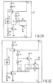
- FIG. 2A shows a further-elaborated version of the feedback circuit F 1 , so as to make it high ohmic and to realize a voltage drop across the transistor T 1 which is as small as possible.
- the feedback circuit F 1 comprises a transistor T 3 , which is a MOS transistor, a bipolar transistor T 4 and a resistor R 1 . Both transistors T 1 and T 3 are of the same type, MOSfet or jFET.
- the gate terminal of the transistor T 1 is coupled to the terminal t 1 of the feedback circuit.
- the terminal t 1 is coupled to the gate terminal of the third transistor T 3 via the resistor R 1 .
- the source terminal of the third transistor T 3 is coupled to the emitter terminal of the fourth transistor T 4 .
- the base terminal of the transistor T 4 is coupled to the terminal t 2 of the feedback circuit, which terminal is coupled to the terminal 6 of the amplifier circuit.
- the gate and drain terminal of the transistor T 3 are interconnected so as to form a diode. Further, the interconnected gate and drain terminals are coupled to the point 12 of constant potential via a current source 21.
- the emitter of the transistor T 4 is coupled to the first point of constant potential 13 via a current source 24. Further, the collector of the transistor T 4 is coupled to the second point of constant potential 12.
- the current sources provide current supply for the transistors T 3 and T 4 .
- the impedance formed by the feedback circuit between the terminals t 1 and t 2 is high-ohmic so as to obtain the desired low value for the cut-off frequency of the lower band edge of the frequency characteristic of the amplifier circuit.
- the circuit of Figure 2A has current sources coupled to both the positive (12) as the negative (13) supply voltage terminal.
- Figure 2B shows a further elaborated version of the feedback circuit of Figure 2A, which has current sources connected to the positive supply terminal only.
- the circuit of Figure 2B further comprises a diode arrangement 25 of one or more diodes, a bipolar transistor T 24 , a current source 22 and a resistor R 24 .
- the current source 22 is coupled between the point 12 of constant potential and the collector of the transistor T 4 , and is further coupled via the diode arrangement 25 to the base terminal of the transistor T 24 .
- the base terminal of the said transistor is also coupled to the point 13 of constant potential via the resistor R 24 .
- the emitter of the transistor T 24 is coupled to the point 13 of constant potential, and its collector is coupled to the interconnected emitter and source of the transistors T 4 and T 3 respectively.
- the circuit part formed by the elements 22, 25, R 24 and T 24 effectively replaces the current source 24 in Figure 2A.
- the circuits of the Figures 2A and 2B further show a switch S 1 connected in parallel to the resistor R 1 .
- the capacitor C 1 When activating the amplifier circuit of Figure 1, or when the current value through the MR element should be changed, the capacitor C 1 must initially be charged (or discharged) so that the amplifier circuit can settle to the new situation. In order to settle fast, the resistor R 1 is short-circuited by the switch S 1 under the influence of a switching signal applied to the control signal input 100, so that the current for charging the capacitor C 1 can be supplied by the current source 21, or discharging can take place via the current source 24.
- the charging time of the capacitor C 1 is thus limited by the maximum current that can be supplied by the current source 21, and the discharging time is limited by the maximum current that can be received by the current source 24.
- Figure 2C shows a feedback circuit in which the charging time of the capacitor C 1 can be shortened.
- the circuit of Figure 2C further comprises a MOS transistor T 5 , a bipolar transistor T 6 and a bipolar diode element 40.
- the gate and drain terminals of the transistor T 5 are interconnected and both coupled to the current source 21 and to a base terminal of the transistor T 6 via the diode element 40.
- the source terminals of the transistors T 3 and T 5 are interconnected.
- a collector terminal of the transistor T 6 is coupled to point 12 of constant potential.
- An emitter terminal of the transistor T 6 is coupled to the interconnected gate and drain terminals of the transistor T 3 .
- the circuit comprising the transistors T 3 , T 6 and T 5 and the diode element 40 form a class-A/B circuit and provides a quicker charging of the capacitor element C 1 during initialisation of the arrangement by means of current supplied by the transistor T 6 .
- FIG 3A shows a further-elaborated version of the amplifier circuit 1 of Figure 1.
- the circuit of Figure 3A comprises a bipolar transistor T 8 , which has its base terminal coupled to the source terminal of the transistor T 1 , its collector to the point 13 of constant potential, and its emitter coupled to the reference point 10. Further a current source 36 is coupled between the reference point 10 and the second point 12 of constant potential.
- This circuit has the advantage that the DC voltage present at the reference point 10 follows the DC voltage present at the terminal 7 of the amplifier circuit. This means that voltage variations occurring across the MR element R m1 do not appear across the load resistor R l1 .
- the voltage difference between the terminals 7 and 10 is equal to V d . If F 1 is one of the circuits of the Figures 2A, 2B or 2C, the voltage difference between the terminals 6 and 7 equals V d + V ch1 - V ch2 , see above, so that the DC offset across the load resistor R l1 is low (V ch1 - V ch2 ). Only voltage variations in the transistor T 1 , resulting from the current variations through the transistor T 1 , still appear across the load resistor R l1 .
- the amplifier circuit 1 further has a MOS transistor T 10 and a bipolar transistor T 11 .
- the gate of transistor T 10 is connected to the gate of the transistor T 1 , the drain is coupled to the point 12 of constant potential via a current source 54, as well as coupled to the base of the transistor T 11 via a diode arrangement 44 consisting of one or more series connected diodes.
- the source of the transistor T 10 is coupled to the collector of the transistor T 11 as well as to the base of the transistor T 8 .
- the emitter of the transistor T 11 is coupled to the point 13 of constant potential.
- the voltage difference between the gate of the transistor T 1 and the terminal 10 equals V gs - V d , where V gs is the gate-source voltage of the transistor T 10 .
- F 1 is again one of the circuits of the Figures 2A, 2B or 2C
- the voltage difference between the gate of the transistor T 1 and terminal 6 equals V gs ' - V d , where V gs ' is the gate-source voltage of the transistor T 3 .
- the voltage across the load resistor R l1 now equals V gs ' - V gs . If the current through transistor T 10 is made equal to the current through the transistor T 3 , and further the transistors T 10 and T 3 have equal dimensions, the said voltage becomes practically zero, independent of the value of the MR bias current.
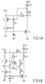
- FIG 4A shows a further improvement of the amplifier circuit of Figure 3A.
- the amplifier circuit comprises a bipolar transistor T 7 which is coupled between the drain terminal of the transistor T 1 and the terminal 6. Its base terminal is coupled to the point 12 of constant potential via the current source 36, and to the point 10 via a resistor R 5 .
- the transistor T 1 is cascoded in order to get a higher output impedance at the terminal 6 and to prevent the Millering of the drain-gate capacitance of transistor T 1 .
- Figure 4B shows an alternative of the amplifier circuit of Figure 4A. It additionally comprises a transistor T 9 , resistors R 2 , R 3 and R 4 and a current source 31.
- the base terminal of the transistor T 7 is connected to an emitter terminal of the transistor T 9 , a base terminal of which is coupled to the source terminal of the transistor T 1 via the resistor R 2 .
- the collector of the transistor T 9 is coupled to the point 13 of constant potential.
- the emitter of the transistor T 9 is further coupled to the point 12 of constant potential via the current source 31.
- the base of the transistor T 9 is coupled to the emitter of the transistor T 8 via the resistor R 3 , and to the reference point 10 via the resistors R 3 and R 4 .
- the construction of the transistors T 7 and T 9 provides a voltage at the interconnection node 32 of the emitter of transistor T 7 and the drain of transistor T 1 , which is roughly half way between the voltages present on the terminals 7 and 6. This means that a voltage difference of V d /2 is present between the node 32 and the terminal 7, and between the nodes 32 and the terminal 6, as the voltage difference between the terminals 6 and 7 is V d , as explained previously.
- Figure 4A and Figure 4B are derived from Figure 3A by adding the cascode transistor T 7 , using different biasing schemes. The same cascode principles can be added to the circuit of Figure 3B.
- Figure 5 shows another embodiment of the amplifier circuit.
- the amplifier circuit of Figure 5 is a further elaboration of the circuit of Figure 3B. Also in this case cascoding can be applied.
- the amplifier circuit of Figure 5 differs from the amplifier circuit of Figure 3B in that it further comprises an impedance network 71. Further, diode 46 and a capacitor element C 3 are present. An emitter terminal of the transistor T 8 is coupled to the first terminal 6 of the amplifier circuit via the impedance network 71, as well as to an output terminal of the current source 36. The collector terminal of the transistor T 8 is coupled to a terminal of the load impedance R l1 '. From the Figure, it appears that the reference point 10 in Figure 3B has now become the reference point 10', which has the same potential as the first point 13 of constant potential, that is ground.
- the base terminal of the transistor T 11 is coupled via the diode 46 to the point 13 of constant potential.
- the base terminal of the transistor T 8 is coupled to the first point 13 of constant potential via the capacitor element C 3 .
- Signal currents I s generated by the MR element R m1 flow from the MR element R m1 to the terminal 7, via the transistor T 1 , the impedance network 71 and the transistor T 8 to the load impedance R l1 , the terminals 48,48' now forming the output terminal of the arrangement.
- the capacitor element C 3 filters out a noise component that would otherwise be present in the output signal at the output terminal 48,48'.
- each MR element is coupled to an amplifier circuit of a type as described above. The output of such an arrangement is then formed by the terminals 48 of each of the two amplifier circuits.
- Figure 6 shows an embodiment of an arrangement which is in the form of a balanced circuit, and comprises two MR elements.
- the arrangement comprises a read head having a first and a second magneto-resistive element R m1 and R m2 respectively. Both MR elements R m1 and R m2 of the head scan the same track (not shown), so that they read the same signal from the track.
- the left hand part of the circuit shown in Figure 6 is largely identical to the circuit diagram shown in Figure 1.
- a first terminal 63 of the MR element R m2 is connected to the first point 13 of constant potential (ground).
- a second bias-current generator 62 is available, having an output for supplying a second bias current (I b2 ).
- the amplifier circuit 61 has a first terminal 66 coupled to the output of the second bias-current generator 62 and a second terminal 67 coupled to the second terminal 64 of the second magneto-resistive element R m2 .
- the second bias-current generator 62, the second amplifier circuit 61 and the second magneto-resistive element R m2 form a series arrangement between the terminals 12 and 13.
- the second amplifier circuit 61 comprises a transistor T 2 , which is in the form of a MOS transistor, a load impedance R l2 , a feedback circuit F 2 and a capacitor element C 2 .
- the source terminal of the transistor T 2 is coupled to the second terminal 67 of the amplifier circuit 61.
- the drain terminal of the transistor T 2 is coupled to the first terminal 66 of the amplifier circuit 61.
- the gate terminal of the transistor T 2 is coupled to the first terminal 66 of the amplifier circuit 61, via the feedback circuit F 2 .
- the gate terminal of the transistor T 2 is coupled to the source terminal of the transistor T 1 via the second capacitor element C 2 .
- the gate terminal of the transistor T 1 is coupled to the source terminal of the transistor T 2 via the capacitor element C 1 .
- a load impedance R l2 is coupled between the terminal 66 of the amplifier circuit 61 and a reference point 10", on which point a reference voltage V ref2 is available.
- the voltage V ref2 may differ from the voltage V ref1 , as the DC voltages across the MR elements R m1 and R m2 can be different owing to mismatch of the resistance of the MR elements and/or unequal MR bias currents I b1 and I b2 .
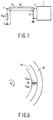
- Figure 7 shows a further improvement of the arrangement having only one MR element.
- Figure 7 shows the provision of an electro-magnetic shielding 75 over the electrical connection 76 connecting the terminal 4 of the MR element R m1 with the terminal 7 of the amplifier circuit 1.
- the shielding 75 is connected to ground via the electrical connection 77.
- This shielding prevents electro-magnetic stray fields from disturbing the signals read out by means of the head.
- the shielding can be realized by means of a kind of coaxial cable. However, also simpler constructions can be used for the shielding means, for instance by wrapping the ground conductor around the signal carrying conductor.
- Figure 8 shows a top view of the reading out of information from a track on the disk shaped record carrier 80, by means of a read head having two MR elements. Both MR elements R m1 and R m2 are coupled together via an insulating layer 90 and both read the full width of the same track 81.
- the arrangements disclosed are preferably intended for hard disk applications, for low supply voltages, such as 3.3 V ⁇ 10% and 5.0 V ⁇ 10%.
- the bias current can be kept low, as the bias current is practically only needed for the MR element.
- a low-noise amplification of the signals read out can be obtained.
- the record carrier is preferably connected to ground via an electrical connection.
- Figures 9A and 9B show units that can be coupled together in order to realize a multiplexed read out of information from a track on a record carrier by means of two or more MR elements.
- Figure 9A shows the circuit part which is common to all MR elements and
- Figure 9B shows the circuit part for each MR element. Only one such circuit part for the MR element R m1 is shown. For other MR elements the circuit part of Figure 9B should be copied.
- the common circuit part of Figure 9A shows at the left side of the vertical broken line a circuit part indicated by the reference numeral 100, which circuit part is largely resembles the feedback circuit of Figure 2C. It lacks the resistor R 1 and the switch S 1 , which are included in the circuit part shown in Figure 9B.
- the circuit part 101 largely resembles the amplifier circuits of Figure 4A and 5.
- Two or more of the circuits of Figure 9B can be coupled to the common circuit of Figure 9A by interconnecting the terminal k 1 ' of the common circuit of Figure 9A with the terminals k 1 of the two or more circuit parts of Figure 9B. In the same way the terminals k 2 and k 2 ', k 3 and k 3 ', and k 4 and k 4 ' are interconnected. Multiplexing is realized by means of the switches S 2 in each of the circuits of Figure 9B. One of the switches S 2 of one of the circuits of Figure 9B coupled to the common circuit of Figure 9A, is opened and the switches S 2 of the other circuits of Figure 9B are closed. In that situation, all of the MR elements R m1 are switched off except one, so that the signal read by that MR element is applied to and amplified by the circuit part of Figure 9A.
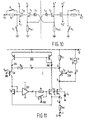
- Figure 10 shows the circuit part of a balanced version of the head, comprising two MR elements R m1 and R m2 , in a fashion as shown in Figure 6, where multiplexing is made possible.
- Figure 10 shows the circuit part including the two MR elements R m1 , R m2 that is separate for each of the heads comprising two MR elements.
- the circuit part is largely mirror symmetrical, where the left hand part, left from the vertical broken line in Figure 10, is the same as the circuit part of Figure 9B.
- the circuit part of the transistors T 1 and T 2 and the capacitors C 1 and C 2 is identical to the corresponding circuit part of those elements in Figure 6.
- the circuit part of Figure 9A is doubled, so as to obtain the common circuit part for each of the heads.
- the circuit part of Figure 9A is thus coupled to the left hand part of the circuit of Figure 10, as has been explained above for the interconnection between the circuits of Figure 9A and 9B.
- the right hand circuit part of Figure 10 is coupled to a circuit part identical to the circuit part of Figure 10A.
- Switching the head of Figure 10 into the circuit means that both switches S 2 and S 3 are in the open position as shown. Consequently, the corresponding switches S 2 and S 3 of the other heads coupled to the common circuit are in their closed position. Switching the head off is realized by closing both switches S 2 and S 3 .
- FIG 11 shows an alternative further-elaborated version of the amplifier circuit 1 of Figure 1.
- the first terminal 6 of the amplifier circuit 1 is directly connected to the output 5 of the bias current generator 2.
- the terminal 8 which interconnects the load impedance R 11 and the feedback circuit F 1 , is connected to the drain of the transistor T 1 via the collector-emitter path of a NPN transistor T 31 .
- the emitter of transistor T 31 is connected to the drain of transistor T 1 , the base is connected to a reference point 308 which supplies a reference voltage V ref4 and the collector is coupled to the load impedance R l1 .
- the transistors T 1 and T 31 form a cascoded output stage.
- the collector of transistor T 31 may be connected to the load impedance R l1 via the collector-emitter path of an optional further NPN cascode transistor (not shown).
- the feedback circuit F 1 between the terminals t 2 , which is connected to the output terminal 8, and the terminal t 1 , which is connected to the gate of transistor T 1 comprises a current mirror 300; a PNP transistor T 30 , having its emitter coupled to an output terminal 304 of the current mirror 300 and having its base connected to a reference voltage terminal 306 to receive a reference voltage V ref3 ; a series resistor R a connected between the emitter of the transistor T 30 and the output terminal 8 of the amplifier circuit 1; a diode connected transistor T 32 of the same type as transistor T 1 , having its source connected to the source of transistor T 1 and its drain coupled to the collector of transistor T 30 ; a transistor T 33 , also of the same type as transistor T 1 , having its gate and source connected to the gate and source of the transistor T 1 and having its drain coupled to an input terminal 30
- the resistance of resistor R 1 is typically 1 MOhm, the capacitance of the capacitor C 1 is typically 200 pF, values that can be integrated.
- the bias current generator 2 can be implemented with a programmable current output digital to analog converter (IDAC) for supplying the bias current of the magneto-resistive element R m1 .
- IDAC programmable current output digital to analog converter
- the IDAC supplies the variable part of the MR element's bias current, for instance 0 mA to 15.5 mA in steps of 0.5 mA, whereas a fixed current, for example 5 mA, is provided by the low-ohmic cascode output stage T 31 .
- transistor T 1 should be large.
- the advantages of the cascoding arrangement are: (1) the large low-noise MOS transistor T 1 and the IDAC can have a low output impedance, since they feed their respective currents into a very low-ohmic emitter of the cascode transistor T 31 ; (2) the drain-to-gate capacitance of the large transistor T 1 is not Millered; (3) the IDAC provides lower bias current and a corresponding lower noise; and (4) the IDAC feeds its current to a low voltage node, which permits a high voltage drop across the IDAC which results in a further reduction of noise.
- the transistors T 32 and T 33 are small in respect of transistor T 1 , but are of the same type.
- the gate-source voltage of transistor T 1 is copied to transistor T 32 by means of transistor T 33 and current mirror 300. Therefore on both sides of resistor R 1 the DC voltages with respect to ground are substantially equal.
- a suitable control signal closes the switch S 1 across resistor R 1 and buffer amplifier 310 provides the high charge or discharge current for recharging capacitor C 1 . Only passive components, i.e. the resistor R 1 , are short circuited during settling.
- the current in resistor R 1 After settling the current in resistor R 1 is zero.
- the current in resistor R a is zero as well, because any current through resistor R a is counteracted by an increased or decreased current through transistor T 1 until the current through resistor R a is zero.
- the voltage at the output terminal 8 is equal to the reference voltage V ref3 at the base of transistor T 30 plus the base-emitter voltage V be of transistor T 30 .
- the voltage drop across the load resistor R 11 is thus equal to V cc -D-V ref3 . This means that the fixed part of the bias current through the MR element can be adjusted by means of the reference voltage V ref3 .
- Figure 12 shows an example of a voltage follower 310 for use in the arrangement of Figure 11.
- the input 400 of the follower 310 is connected to the base of a PNP transistor T 41 .
- the emitter of this transistor is coupled to the point 12 of constant potential via the series arrangement of a resistor 402 and a bias current source 404.
- the collector of transistor T 41 is connected to point 13 (ground) via a series arrangement of a diode connected PNP transistor T 42 and a resistor 406.
- the resistors 402 and 406 have equal resistances.
- the transistors T 41 and T 42 have equal emitter areas.
- the voltage drop U 1 caused by current source 404 across the series arrangement of the base-emitter junction of transistor T 41 and resistor 402 is equal to the voltage drop across the series arrangement of the diode connected transistor T 42 and resistor 406.
- the interconnection node of the current source 404 and the resistor 402 is connected to the base of a NPN transistor T 43 .
- the collector of this transistor is coupled to point 12 and the emitter is connected to the output 408 of the follower 310 via a resistor 410.
- the interconnection node of collector of transistor T 42 and the series connection of transistor T 42 and resistor 406 is connected to the base of a NPN transistor T 44 , the collector of which is connected to the output 408 and the emitter of which is connected to ground via a resistor 412.
- the resistors 410 and 412 have equal resistances and the transistors T 43 and T 44 have equal dimensions. In steady state the voltage drop U 1 across the series arrangement of the base-emitter junction of transistor T 44 and resistor 412 is equal to the voltage drop across the series arrangement of the base-emitter junction of transistor T 43 and resistor 410.
- the switch S 1 in the arrangement shown in Figure 11 can be implemented conventionally with a MOS transistor.
- the main inaccuracy which is still left then is caused by charge injection of the switch S 1 into the capacitor C 1 .
- the switch S 1 is opened and some capacitive charge is extracted from capacitor C 1 .
- This charge is about equal to half the charge in the channel of the MOS transistor.
- This charge extraction would be normally compensated by switching a small additional capacitor which is connected between capacitor C 1 and point 12. However, this causes crosstalk from the supply voltage to the capacitor C 1 .
- FIG 13 shows a MOS switching arrangement S 1 which feeds half of the channel charge back to capacitor C 1 and compensates the charge extraction from capacitor C 1 .
- the switch S 1 is composed of first, ST 1 , and second, ST 2 , NMOS switching transistors.
- the source of the first switching transistor ST 1 is connected to the drain of the second switching transistor ST 2
- the drain of the first switching transistor ST 1 is connected to the source of the second switching transistor ST 2 .
- the switching transistors ST 1 and ST 2 are driven by first, DT 1 , and second, DT 2 , PMOS driver transistors. These PMOS transistors have sources connected to the point 12 and have gates connected to the control input 100 for receiving a control signal.
- the drain of the first driver transistor DT 1 is connected to the gate of the first switching transistor ST 1
- the drain of the second driver transistor DT 2 is connected to the gate of the second switching transistor ST 2
- third DT 3 and fourth DT 4 NMOS driver transistors are provided. These NMOS driver transistors have their gates connected to the control input 100, whereas the source of the third driver transistor DT 3 is connected to the drain of the first switching transistor ST 1 , the source of the fourth driver transistor DT 4 to the drain of the second switching transistor ST 2 , the drain of the third driver transistor DT 3 to the drain of the first driver transistor DT 1 , and the drain of the fourth driver transistor DT 4 to the drain of the second driver transistor DT 2 .
- the PMOS driver transistors DT 1 and DT 2 are conductive and switch on the switching transistors ST 1 and ST 2 and resistor R 1 is short-circuited for fast settling.
- the settling is finished by applying a high voltage at the control terminal 100.
- the PMOS driver transistors DT 1 and DT 2 are cut off and the NMOS driver transistors DT 3 and DT 4 are made conductive.
- the conductive driver transistor DT 3 provides a conduction path from the gate of the switching transistor ST 1 to the capacitor C 1 and allows half the channel charge of switching transistor ST 1 to flow into the capacitor C 1 , thereby cancelling the half of the channel charge of switching transistor ST 2 which is extracted from the capacitor C 1 .
- Figure 14 shows a balanced version of the arrangement of Figure 11.
- the two amplifiers 1 and 61 in particular the capacitors C 1 and the corresponding capacitor C 2 of the second amplifier 61, are interconnected in a similar fashion as shown in Figure 6.
- the capacitors C 1 and C 2 form a short circuit and shunt the two individual equivalent source noise resistors R n of the MOS transistors T 1 and T 2 .
- R n is about equal to R o , R o being the inverse of the transconductance of the transistors T 1 and T 2 .
- the total effective noise resistance in the first amplifier 1 of the arrangement of Figure 12 is R m1 +R n /2 instead of R m1 +R n of the first amplifier 1 of the arrangement of Figure 11.
- the balanced version thus provides a reduction of noise.
- One of the MR elements R m1 or R m2 may be omitted when using single stripe MR read heads. In that case terminal 7 or 67 is coupled to ground 13.
- the input terminals of the current mirrors may be advantageously interconnected to cancel signal components.
- two further switches are provided in each half of the balanced arrangement.
- One further switch S 2 for connecting the gate of transistor T 1 to ground and a second parallel-operated further switch S 3 for connecting the gate of transistor T 32 to ground.
- Similar switches are provided which are operated simultaneously with switches S 2 and S 3 .
- Elements which have to be duplicated for each dual read head are enclosed by a dashed line.
- the remainder of the balanced arrangement is common to all dual read heads.
- a dual read head is disabled by closing the switches S 3 and S 4 in both parts of the balanced arrangement. Fast settling is obtained by closing the switches S 1 temporarily.
- transistors T 1 , T 2 , T 3 , T 5 and T 10 are preferably unipolar MOS transistors; other transistors such as the transistors T 4 , T 24 , T 6 , T 7 , T 8 , T 9 , T 11 and T 31 , are preferably bipolar transistors. It is, however, possible to use bipolar transistors instead of unipolar transistors and vice versa, or to use only bipolar or only unipolar transistors.
- the first main flow terminal, the second main flow terminal and the control terminal of a transistor correspond to, respectively, the source terminal, the drain terminal and gate terminal of an unipolar transistor and to, respectively, the emitter terminal, the collector terminal and base terminal of a bipolar transistor.
Landscapes
- Amplifiers (AREA)
Description
a series resistor Ra connected between the emitter of the transistor T30 and the
Claims (13)
- Arrangement for reading out an information signal from a magnetic record carrier, comprising:a read head having a magneto-resistive element (Rm1) with a first terminal (3) connected to a first point (13) of constant potential, and with a second terminal (4),a bias-current means (2; T30,T31) for supplying a bias-current,an amplifier circuit (1) comprising an output terminal (8) for supplying the information signal (Vout), a first terminal (6) coupled to the bias-current means (2; T30,T31) and to the output terminal (8), a second terminal (7) coupled to the second terminal (4) of the magneto-resistive element (Rm1) so as to form a series arrangement of the bias-current means (2; T30,T31), the amplifier circuit (1) and the magneto-resistive element (Rm1) between a second point (12) of constant potential and said first point (13) of constant potential, the amplifier circuit (1) further comprising a first transistor (T1), a feedback circuit (F1) having an input terminal (t2) coupled to the output terminal (8) of the amplifier circuit (1) and having an output terminal (t1), a load impedance (Rl1) and a capacitor element (C1), a first main flow terminal of the first transistor (T1) being connected to the second terminal (7) of the amplifier circuit (1), a second main flow terminal of the first transistor (T1) being coupled to the first terminal (6) of the amplifier circuit (1), a control terminal of the first transistor (T1) being coupled to the output terminal (t1) of the feedback circuit (F1), the control terminal being further coupled to the first point (13) of constant potential via at least the capacitor element (C1), the load impedance (Rl1) being coupled to the output terminal (8) of the amplifier circuit (1), characterized in that the feedback circuit comprises:voltage buffer means having an input coupled to the input terminal (t2) of the feedback circuit (F1) and having an output;a first series resistor (R1) connected between the output of the voltage buffer means and the output terminal (t1) of the feedback circuit (F1); anda switch (S1) connected in parallel with the first series resistor (R1) and operable in response of a control signal.
- Arrangement as claimed in claim 1, characterized in that the voltage buffer means comprises a first current source (24) and a second current source (21), a second (T3) transistor having a control terminal connected to a second main flow terminal and a third transistor (T4), a first main flow terminal of the second transistor (T3) and a first main flow terminal of the third transistor (T4) being interconnected and coupled to the first point (13) of constant potential via the first current source (24), the second main flow terminal of the second transistor (T3) being coupled to the second point (12) of constant potential via the second current source (21) and forming the output of the voltage buffer means, a second main flow terminal of the third transistor being coupled to the second point (12) of constant potential, and a control terminal of the third transistor (T4) forming the input of the voltage buffer means and being coupled to the input terminal (t2) of the feedback circuit (F1).
- Arrangement as claimed in claim 2, characterized in that the voltage buffer means further comprises a third current source (22) connected between the second main flow terminal of the third transistor (T4) and the second point (12) of constant potential and in that the first current source (2) comprises a diode arrangement (25), a bias resistor (R24) and a fourth transistor (T24) having a first main flow terminal connected to the first point (13) of constant potential, a second main flow terminal connected to first main flow terminals of the second (T3) and third (T4) transistors and a control terminal coupled to the second main flow terminal of the third transistor (T4) via the diode arrangement (25) and to the first point (13) of constant potential via the bias resistor (R24).
- Arrangement as claimed in claim 3, characterized in that the voltage buffer means further comprises a fifth transistor (T5) and a diode element (40), a control terminal and a second main flow terminal of the fifth transistor (T5) being interconnected and being coupled to the third current source (21) via the diode element (40), a first main flow terminal of the fifth transistor (T5) being connected to the first main flow terminal of the second transistor (T3), and a sixth transistor (T6) having a first main flow terminal coupled to the second main flow terminal of the second transistor (T3), a second main flow terminal coupled to the second point (12) of constant potential and a control terminal coupled to the second main flow terminal of the fifth transistor (T5) via the diode element (40).
- Arrangement as claimed in claim 1, 2, 3 or 4, characterized in that the amplifier circuit comprises a seventh transistor (T7) having a first main flow terminal connected to the second main flow terminal of the first transistor (T1) and a second main flow terminal coupled to the first terminal (6) of the amplifier circuit (1).
- Arrangement as claimed in claim 1, 2, 3, 4 or 5, characterized in that the amplifier circuit (1) comprises an eighth transistor (T8) having a control terminal coupled to the second terminal (7) of the amplifier circuit (1), a first main flow terminal coupled to the second point (12) of constant potential via a bias current source (36), and a second main flow terminal coupled to the first point (13) of constant potential, the load impedance (Rl1) being coupled between the output terminal (8) of the amplifier circuit (1) and the first main flow terminal of the eighth transistor (T8).
- Arrangement as claimed in claim 5 and 6, characterized in that the amplifier circuit (1) further comprises a ninth transistor (T9) having a first main flow terminal coupled to a control terminal of the seventh transistor (T7) and a control terminal coupled to the first main flow terminal of the eighth transistor (T8).
- Arrangement as claimed in claim 7, characterized in that the amplifier circuit (1) further comprises a tenth transistor (T10) having a control terminal coupled to the control terminal of the first transistor (T1) and having a first main flow terminal coupled to the control terminal of the eighth transistor (T8).
- Arrangement as claimed in claim 6, 7 or 8, characterized in that the second main flow terminal of the eighth transistor (T8) is coupled to the first point (13) of constant potential via a further load impedance (Rl1') for providing the information signal.
- Arrangement as claimed in claim 1, characterized in that the first terminal (6) is coupled to the output terminal (8) of the amplifier circuit (1) via a second transistor (T31) having a first main flow terminal connected to the first terminal (6) and a second main flow terminal coupled to the output terminal (8) of the amplifier circuit (1); and in that the voltage buffer means comprises:a current mirror (300) having an input terminal (302) and an output terminal (304),a third transistor (T30) having a conductivity opposite to the conductivity of the second transistor (T31) and having a first main flow terminal coupled to the output terminal (304) of the current mirror (300) and a control terminal connected to receive a reference voltage,a second series resistor (Ra) connected between the first main flow terminal of the third transistor (T30) and the output terminal (8) of the amplifier circuit (1),a fourth transistor (T32) of the same type as the first transistor (T1) having a control terminal connected to a second main flow terminal, andhaving a first main flow terminal connected to the first main flow terminal of the first transistor (T1) and a second main flow terminal coupled to a second main flow terminal of the third transistor (T30),a fifth transistor (T33) of the same type as the first transistor (T1) having a control terminal and a first main flow terminal connected to the corresponding terminals of the first transistor (T1) and having a second main flow terminal coupled to the input terminal (302) of the current mirror (300); and a buffer amplifier (310) having an input connected to the control terminal of the fourth transistor (T32) and an output connected to the first series resistor (R1).
- Arrangement as claimed in claim 10, characterized in that the bias current means comprises a bias current generator (2) having an output (5) connected to the first terminal (6) of the amplifier circuit (1).
- Arrangement as claimed in claim 1, 2, 3, 4, 5, 6, 7, 8, 9, 10 or 11, characterized in that the switch (S1) comprises:
first (ST1) and second (ST2) switching transistors of a first conductivity type, a first main flow terminal of the first switching transistor (ST1) being connected to a second main flow terminal of the second switching transistor (ST2), a second main flow terminal of the first switching transistor (ST1) being connected to a first main flow terminal of the second switching transistor (ST2); first (DT1) and second (DT2) driver transistors of a second conductivity type having first main flow terminals connected to a supply voltage terminal (12) and having control terminals connected to a control input (100) for receiving the control signal, a second main flow terminal of the first driver transistor (DT1) being connected to the control terminal of the first switching transistor (ST1), a second main flow terminal of the second driver transistor (DT2) being connected to the control terminal of the second switching transistor (ST2); third (DT3) and fourth (DT4) driver transistors of the first conductivity type having control terminals connected to the control input (100), a first main flow terminal of the third driver transistor (DT3) being connected to the second main flow terminal of the first switching transistor (ST1), a first main flow terminal of the fourth driver transistor (DT4) being connected to the second main flow terminal of the second switching transistor (ST2), a second main flow terminal of the third driver transistor (DT3) being connected to the second main flow terminal of the first driver transistor (DT1), a second main flow terminal of the fourth driver transistor (DT4) being connected to the second main flow terminal of the second driver transistor (DT2). - An arrangement as claimed in any of the preceding claims, further comprising a second arrangement, substantially identical to the first mentioned arrangement, the capacitor element (C1) of the amplifier circuit (1) of the first arrangement being coupled to the second terminal (67) of the amplifier circuit (61) of the second arrangement and the capacitor element (C2) of the amplifier circuit (61) of the second arrangement being coupled to the second terminal (7) of the amplifier circuit (1) of the first arrangement.
Priority Applications (1)
| Application Number | Priority Date | Filing Date | Title |
|---|---|---|---|
| EP94926362A EP0672260B1 (en) | 1993-10-06 | 1994-09-23 | Arrangement for reading information from a track on a record carrier comprising a fast settling read amplifier for magneto-resistive heads |
Applications Claiming Priority (6)
| Application Number | Priority Date | Filing Date | Title |
|---|---|---|---|
| EP93202836 | 1993-10-06 | ||
| EP93202836 | 1993-10-06 | ||
| EP94201806 | 1994-06-23 | ||
| EP94201806 | 1994-06-23 | ||
| PCT/IB1994/000292 WO1995010050A1 (en) | 1993-10-06 | 1994-09-23 | Arrangement for reading information from a track on a record carrier comprising a fast settling read amplifier for magneto-resistive heads |
| EP94926362A EP0672260B1 (en) | 1993-10-06 | 1994-09-23 | Arrangement for reading information from a track on a record carrier comprising a fast settling read amplifier for magneto-resistive heads |
Publications (2)
| Publication Number | Publication Date |
|---|---|
| EP0672260A1 EP0672260A1 (en) | 1995-09-20 |
| EP0672260B1 true EP0672260B1 (en) | 2001-10-17 |
Family
ID=27235337
Family Applications (1)
| Application Number | Title | Priority Date | Filing Date |
|---|---|---|---|
| EP94926362A Expired - Lifetime EP0672260B1 (en) | 1993-10-06 | 1994-09-23 | Arrangement for reading information from a track on a record carrier comprising a fast settling read amplifier for magneto-resistive heads |
Country Status (1)
| Country | Link |
|---|---|
| EP (1) | EP0672260B1 (en) |
-
1994
- 1994-09-23 EP EP94926362A patent/EP0672260B1/en not_active Expired - Lifetime
Also Published As
| Publication number | Publication date |
|---|---|
| EP0672260A1 (en) | 1995-09-20 |
Similar Documents
| Publication | Publication Date | Title |
|---|---|---|
| US5619386A (en) | Arrangement for reading information from a track on a record carrier comprising a fast settling read amplifier for magneto-resistive heads | |
| EP0586062B1 (en) | Amplifier for magnetoresistive sensor | |
| US6040732A (en) | Switched-transconductance circuit within integrated T-switches | |
| EP0361781B1 (en) | Protective circuit for magnetoresistive element | |
| JP3683277B2 (en) | Device comprising a magnetic write head and write amplifier with capacitive feedforward compensation | |
| US5559646A (en) | Balanced arrangement for reading information from a track on a record carrier which arrangement includes amplifier circuits containing cut-off capacitors which are cross-coupled to reduce noise | |
| US5410274A (en) | Single-ended and differential amplifiers with high feedback input impedance and low distortion | |
| US6218903B1 (en) | Signal amplifier and magnetic disk storage apparatus using the same | |
| JP3773256B2 (en) | Apparatus comprising a magnetic write head and a write amplifier having capacitive current compensation | |
| US6104244A (en) | Amplifier having a rail-to-rail output stage | |
| US6828845B2 (en) | Analogue selector | |
| JPH10513316A (en) | amplifier | |
| US5886568A (en) | Open-loop MR biasing circuit with high power supply and common mode rejection | |
| US6150876A (en) | Voltage bias, current sense preamplifier for a magnetoresistive reader | |
| KR100818813B1 (en) | Current mirror circuit, integrated circuit and optical recording medium reproducing apparatus | |
| US6226137B1 (en) | Voltage bias, current sense preamplifier using no AC-coupling capacitors for a dual strip magnetoresistive reader | |
| EP0672260A1 (en) | Arrangement for reading information from a track on a record carrier comprising a fast settling read amplifier for magneto-resistive heads | |
| US6211736B1 (en) | Signal amplifying circuit for magnetoresistive element | |
| US6275347B1 (en) | Current bias, current sense preamplifier for a magnetoresistive reader | |
| JP2001067602A (en) | MR element signal amplifier circuit | |
| EP0459579B1 (en) | Read head arrangement comprising 2n read heads of the MR type, and reproduction arrangement comprising the read head arrangement | |
| EP0672259B1 (en) | Arrangement for reading information from a track on a record carrier | |
| KR20000062710A (en) | Readback amplifier for wideband readout of magneto-resistive heads for data storage | |
| EP0107248B1 (en) | Switching amplifier | |
| US6208482B1 (en) | Signal amplifying circuit for an MR element |
Legal Events
| Date | Code | Title | Description |
|---|---|---|---|
| PUAI | Public reference made under article 153(3) epc to a published international application that has entered the european phase |
Free format text: ORIGINAL CODE: 0009012 |
|
| AK | Designated contracting states |
Kind code of ref document: A1 Designated state(s): DE FR GB |
|
| 17P | Request for examination filed |
Effective date: 19951013 |
|
| RAP3 | Party data changed (applicant data changed or rights of an application transferred) |
Owner name: PHILIPS NORDEN AB Owner name: KONINKLIJKE PHILIPS ELECTRONICS N.V. |
|
| 17Q | First examination report despatched |
Effective date: 19991007 |
|
| GRAG | Despatch of communication of intention to grant |
Free format text: ORIGINAL CODE: EPIDOS AGRA |
|
| GRAG | Despatch of communication of intention to grant |
Free format text: ORIGINAL CODE: EPIDOS AGRA |
|
| GRAH | Despatch of communication of intention to grant a patent |
Free format text: ORIGINAL CODE: EPIDOS IGRA |
|
| GRAH | Despatch of communication of intention to grant a patent |
Free format text: ORIGINAL CODE: EPIDOS IGRA |
|
| GRAA | (expected) grant |
Free format text: ORIGINAL CODE: 0009210 |
|
| AK | Designated contracting states |
Kind code of ref document: B1 Designated state(s): DE FR GB |
|
| REF | Corresponds to: |
Ref document number: 69428679 Country of ref document: DE Date of ref document: 20011122 |
|
| REG | Reference to a national code |
Ref country code: GB Ref legal event code: IF02 |
|
| ET | Fr: translation filed | ||
| PLBE | No opposition filed within time limit |
Free format text: ORIGINAL CODE: 0009261 |
|
| STAA | Information on the status of an ep patent application or granted ep patent |
Free format text: STATUS: NO OPPOSITION FILED WITHIN TIME LIMIT |
|
| PG25 | Lapsed in a contracting state [announced via postgrant information from national office to epo] |
Ref country code: GB Free format text: LAPSE BECAUSE OF NON-PAYMENT OF DUE FEES Effective date: 20020923 |
|
| 26N | No opposition filed | ||
| PG25 | Lapsed in a contracting state [announced via postgrant information from national office to epo] |
Ref country code: DE Free format text: LAPSE BECAUSE OF NON-PAYMENT OF DUE FEES Effective date: 20030401 |
|
| GBPC | Gb: european patent ceased through non-payment of renewal fee |
Effective date: 20020923 |
|
| PG25 | Lapsed in a contracting state [announced via postgrant information from national office to epo] |
Ref country code: FR Free format text: LAPSE BECAUSE OF NON-PAYMENT OF DUE FEES Effective date: 20030603 |
|
| REG | Reference to a national code |
Ref country code: FR Ref legal event code: ST |
|
| REG | Reference to a national code |
Ref country code: HK Ref legal event code: WD Ref document number: 1013332 Country of ref document: HK |