EP0667580B1 - Système d'antémémoire pour une mémoire - Google Patents
Système d'antémémoire pour une mémoire Download PDFInfo
- Publication number
- EP0667580B1 EP0667580B1 EP95300681A EP95300681A EP0667580B1 EP 0667580 B1 EP0667580 B1 EP 0667580B1 EP 95300681 A EP95300681 A EP 95300681A EP 95300681 A EP95300681 A EP 95300681A EP 0667580 B1 EP0667580 B1 EP 0667580B1
- Authority
- EP
- European Patent Office
- Prior art keywords
- cache
- data line
- data
- main memory
- memory
- Prior art date
- Legal status (The legal status is an assumption and is not a legal conclusion. Google has not performed a legal analysis and makes no representation as to the accuracy of the status listed.)
- Expired - Lifetime
Links
Images


Classifications
-
- G—PHYSICS
- G06—COMPUTING; CALCULATING OR COUNTING
- G06F—ELECTRIC DIGITAL DATA PROCESSING
- G06F12/00—Accessing, addressing or allocating within memory systems or architectures
- G06F12/02—Addressing or allocation; Relocation
- G06F12/08—Addressing or allocation; Relocation in hierarchically structured memory systems, e.g. virtual memory systems
- G06F12/0802—Addressing of a memory level in which the access to the desired data or data block requires associative addressing means, e.g. caches
- G06F12/0893—Caches characterised by their organisation or structure
- G06F12/0897—Caches characterised by their organisation or structure with two or more cache hierarchy levels
-
- G—PHYSICS
- G06—COMPUTING; CALCULATING OR COUNTING
- G06F—ELECTRIC DIGITAL DATA PROCESSING
- G06F12/00—Accessing, addressing or allocating within memory systems or architectures
- G06F12/02—Addressing or allocation; Relocation
- G06F12/08—Addressing or allocation; Relocation in hierarchically structured memory systems, e.g. virtual memory systems
- G06F12/0802—Addressing of a memory level in which the access to the desired data or data block requires associative addressing means, e.g. caches
- G06F12/0864—Addressing of a memory level in which the access to the desired data or data block requires associative addressing means, e.g. caches using pseudo-associative means, e.g. set-associative or hashing
-
- G—PHYSICS
- G06—COMPUTING; CALCULATING OR COUNTING
- G06F—ELECTRIC DIGITAL DATA PROCESSING
- G06F12/00—Accessing, addressing or allocating within memory systems or architectures
- G06F12/02—Addressing or allocation; Relocation
- G06F12/08—Addressing or allocation; Relocation in hierarchically structured memory systems, e.g. virtual memory systems
- G06F12/12—Replacement control
-
- G—PHYSICS
- G06—COMPUTING; CALCULATING OR COUNTING
- G06F—ELECTRIC DIGITAL DATA PROCESSING
- G06F12/00—Accessing, addressing or allocating within memory systems or architectures
- G06F12/02—Addressing or allocation; Relocation
- G06F12/08—Addressing or allocation; Relocation in hierarchically structured memory systems, e.g. virtual memory systems
- G06F12/0802—Addressing of a memory level in which the access to the desired data or data block requires associative addressing means, e.g. caches
- G06F12/0862—Addressing of a memory level in which the access to the desired data or data block requires associative addressing means, e.g. caches with prefetch
Definitions
- the present invention concerns a cache system for a memory, for example for decreasing time penalty resulting from a cache miss in a multi-level cache system.
- CPU central processing unit
- main memory main memory
- the speed at which the CPU can decode and execute instructions and operands depends upon the rate at which the instructions and operands can be transferred from main memory to the CPU.
- many computer systems include a cache memory between the CPU and main memory.
- a cache memory is a small, high-speed buffer memory which is used to hold temporarily those portions of the contents of main memory which it is believed will be used in the near future by the CPU.
- the main purpose of a cache memory is to shorten the time necessary to perform memory accesses, either for data or instruction fetch.
- the information located in cache memory may be accessed in much less time than information located in main memory.
- a CPU with a cache memory needs to spend far less time waiting for instructions and operands to be fetched and/or stored.
- a cache memory is made up of many blocks of one or more words of data. Each block has associated with it an address tag that uniquely identifies of which block of main memory it is a copy. Each time the processor makes a memory reference, an address tag comparison is made to see if a copy of the requested data resides in the cache memory. If the desired memory block is not in the cache memory, the block is retrieved from the main memory, stored in the cache memory and supplied to the processor.
- the CPU may also write data into the cache memory instead of directly to the main memory.
- the cache memory makes an address tag comparison to see if the data block into which data is to be written resides in the cache memory. If the data block exists in the cache memory, the data is written into the data block in the cache memory. In many systems a data "dirty bit" for the data block is then set. The dirty bit indicates that data in the data block is dirty (i.e., has been modified), and thus before the data block is deleted from the cache memory the modified data must be written into main memory.
- the data block into which data is to be written does not exist in the cache memory, the data block must be fetched into the cache memory or the data written directly into the main memory.
- a data block which is overwritten or copied out of cache memory when new data is placed in the cache memory is called a victim block or a victim line.
- a second cache memory is added in series between the first cache memory and the main memory.
- the first cache memory typically has a subset of the data in the second cache memory.
- the second cache memory typically has a subset of the data in the main memory. Accessed data is first searched for in the first cache memory. If there is a miss in the first cache memory, the accessed data is searched for in the second cache memory. If there is a miss in the second cache memory, the data is fetched from the main memory.
- the first level cache is a proper subset of the second level cache. What is meant by a proper subset is that all entries in the first level cache are also in the second level cache.
- the second level cache has additional entries that are not in the first level cache. It is also smaller and closer to the processor than a second level cache. Since it is smaller and closer to the processor, a first level cache can, in general, offer improved performance because it has a smaller access latency than its companion second level cache or even that of memory.
- a memory reference is generally a load or store instruction.
- the reference might hit in the first level cache.
- a hit is defined as when the data for a desired memory address is present in the cache being checked (first level or second level).
- a miss is defined to be a memory reference where the data for a desired memory address is not present in the cache being checked (first level or second level).
- the next fastest case is a first level cache miss that happens to hit in the second level cache. This causes a sequence of operations to be performed to fill a single first level cache line with the appropriate sixteen byte quantity from the second level cache. Data is subsequently supplied to the processor or the store completes. This is a medium speed operation, and the processor will be frozen while it waits for the memory reference to be satisfied.
- the slowest operation is when the memory reference misses both the first level and second level caches.
- a long sequence of operations is initiated to bring the relevant line from main memory into the second level cache.
- the first level cache is again referenced, resulting, this time, in a first level cache miss that now hits in the second level cache. This causes the relevant portion of the second level cache line to be written into the first level cache, and subsequently the requested data is supplied to the processor, or the store completes.
- cache memories are direct mapped. That is, an index is used to access one or more entries in the cache. The tag for the entry is then compared with the tag portion of the address to determine whether a match has occurred.
- a single index is used to simultaneously access a plurality of data random access memories (RAMs).
- a data RAM may be implemented by one or more physical random access memory integrated circuits.
- a set is a collection of all lines addressed by a single cache index. The number of data RAMs addressed by a single cache index indicates the way number of a cache. For example, if in a cache a single cache index is used to access data from two data RAMs, the cache is a two-way set-associative cache. Similarly, if in a cache a single cache index is used to access data from four data RAMs, the cache is a four-way set-associative cache.
- a tag comparison is made for each data RAM. If a tag comparison indicates the desired data block is in a particular data RAM the operation is performed on/with data from that particular data RAM.
- a fully associative cache no index is used.
- a tag comparison is made for each cache line within the fully associative cache. if a tag comparison indicates the desired data line is in the cache. the operation is performed on/with data from that particular data line.
- a fully associative victim cache receives victim lines from a larger direct mapped cache.
- the fully associative victim cache may sometimes be found in the fully associative victim cache.
- EP-A-0,437,712 discloses a tandem cache memory comprising a first cache for storing a plurality of instructions more recently requested by a processor and for providing them to the processor, following a new request, without need to fetch them from a working memory and a second cache for reading from the working memory and storing a plurality of prefetched instruction blocks having subsequent addresses in increasing order relative to a current instructions requested for execution by the processor and for providing any one of the prefetched instruction blocks to both the processor and the first cache on processor request, if the processor requests an instruction which is not in the first cache but is stored in the second cache.
- An example of a prior art cache system comprises a stream buffer connected in series between a direct mapped cache and a main memory.
- the present invention seeks to provide an improved cache system.
- a cache system buffers data stored in a main memory and utilized by a processor.
- the cache system includes a first cache, a second cache, first transfer means, second transfer means, third transfer means, and an access means.
- the first cache is fully associative.
- the second cache is directly mapped.
- the first transfer means transfers data lines from the main memory to the first cache.
- the second transfer means transfers data lines from the first cache to the second cache.
- the third transfer means transfers data lines from the second cache to the main memory. Accesses of data lines from the first cache and the second cache are performed in parallel.
- a hash function is used to generate an index into the second cache, in which a tag for a data line accessed by the index is compared with a tag for a desired data line to determine whether there as been a hit in the second cache.
- the tags for all data lines in the first cache are checked to determine whether there is a hit.
- a content addressable memory stores tags for the first cache. The data lines are stored by the first cache in a first-in-first-out memory.
- stored with each data line in the first cache is an indication which indicates a destination for the data line when the data line is moved out of the first cache.
- the indication indicates whether the data line is to be moved to the second cache or moved to the main memory.
- data lines are moved out of the first cache two at a time when the first cache contains more than a predetermined number of data lines.
- the two data lines map to a same location in the second cache, one of the two data lines will be moved to the main memory.
- the processor will generate a prefetch address to be used if there is a cache miss, or if there is a hit on a data line in the first cache where a reference bit for the "hit" data line is set to zero. If the data line for the prefetch address is already in the first or second cache no further action need be taken. If the data line for the prefetch address is not already in one of the caches, the data line for the prefetch address will be prefetched. The reference bit for a prefetch data line is cleared (i.e., set to zero), indicating the prefetched data line was unreferenced.
- the reference bit When there is a cache hit on a data line in the first cache that is marked “unreferenced” the reference bit will then be set to one indicating that the data line has now been referenced.
- the data line for the prefetch address when there is a cache hit on a data line in the first cache that is marked "unreferenced” and a prefetch address has been generated, if the data line for the prefetch address is not in one of the caches, the data line for the prefetch address will be prefetched from the main memory and placed in the first cache. The reference bit for the prefetched data line is cleared, indicating the prefetched data line was unreferenced.
- the preferred embodiment can eliminate thrashing behavior typically associated with direct mapped caches with the addition of only a minimal amount of hardware.
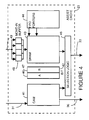
- Figure 1 shows a simplified block diagram of a computer system with a instruction cache and a data cache, in accordance with a preferred embodiment of the present invention.
- FIG 2 shows a simplified block diagram of a processor shown in Figure 1, in accordance with a preferred embodiment of the present invention.
- FIG 3 shows a simplified block diagram of the cache system for data for the computer system shown in Figure 1 in accordance with the preferred embodiment of the present invention.
- FIG 4 shows a simplified block diagram of an assist cache within the processor shown in Figure 2 in accordance with the preferred embodiment of the present invention.
- FIG. 1 shows a simplified block diagram of a computer system.
- a processor 12 and a memory 11 are shown connected to a bus 10.
- Processor 12 utilizes a instruction cache 13 and a data cache 14.
- Instruction cache 13 stores instructions for processor 12 in static random access memory (SRAM).
- Data cache 14 stores data for processor 12 in SRAM.
- FIG. 2 shows a simplified block diagram of processor 12.
- Processor 12 is shown to include system bus interface logic 26, instruction cache interface logic 24, data cache interface logic 25, an arithmetic logic unit (ALU) 22, a translation look aside buffer (TLB) 21, and an assist cache 23.
- System bus interface logic 26 provides processor 12 with an interface to system bus 10.
- Instruction cache interface logic 24 provides processor 12 with an interface to instruction cache 13.
- Data cache interface logic 25 provides processor 12 with an interface to data cache 14.
- assist cache 23 is used in parallel with data cache 14 to provide data to arithmetic logic unit 22.
- Translation look aside buffer 21 is used to map virtual addresses to real addresses in order to generate cache tags to be used to access to data stored within assist cache 23 and within data cache 14.
- Figure 3 shows the organization for the data cache system.
- assist cache 23 consists of 64 fully-associative 32-byte cache lines.
- Assist cache 23 stores tags in a content-addressable-memory (CAM) which allows a portion of an address to be matched with each entry's tag.
- data cache 14 is direct mapped and consists of up to 1 megabytes of data (32K 32-byte cache lines).
- both data cache 14 and assist cache 23 are accessed in parallel.
- the real address accessed from TLB 21 (shown in Figure 2) is used to generate an assist cache access tag for access into assist cache 23. If there is a match of the assist cache access tag with the tag for any data line within assist cache 23, a hit is generated on a data line 36.
- the hit signals a selector 37 to select the "hit" data from assist cache and place the hit data on a data path 33.
- an index 13 is used to access a single data line within data cache 14.
- the index consists of a hashed value derived from hashing a portion of the virtual address for the accessed memory location.
- An address tag for the indexed location in data cache 14 is compared with a portion of the real address of the accessed memory location placed on data lines 31. The comparison is represented by comparison logic 35. If there is a hit from either assist cache 23 or data cache 14, logic 34 generates a hit signal on a hit data line 32.
- both the accessed data line and any prefetched data line will be brought into assist cache 23 with its allocate bit cleared (i.e., set to zero), indicating "no-allocate".
- the reference bit is cleared (see below)
- that preferred data line will be brought into assist cache 23 with the allocate bit cleared to other data lines are brought into assist cache 23 with the allocate bit set to one indicating "allocate”.
- the allocate bit is checked to determine whether the data line is to be moved to data cache 14 or to main memory 11 (if dirty). If the allocate bit for the data line is set to one, the data line is moved to data cache 14. If the allocate bit is set to zero, the data line is moved to main memory 11 if it is dirty (i.e., if it has been modified since being brought into assist cache). If the data line is not dirty, it may be discarded without being written back to main memory 11.
- data lines within assist cache 23 are marked as "no allocate" when the data is not expected to be used for a long period of time, but other pieces of data within the same data line of the data may be used in a short period of time.
- United States Patent Number 4,928,239 issued to William R. Bryg et al. for Cache Memory with Variable Fetch and Replacement Schemes .
- the allocate bit is checked to determine whether the data line is to be moved to data cache 14 or to main memory 11.
- the assist cache 23 is excellent at eliminating cache thrashing without compiler optimizations.
- Entries within assist cache 23 are ordered in a circulating FIFO queue. New data lines requested from main memory 11 due to a cache miss or a prefetch are placed at the top of the queue and old entries are moved out the bottom. Flushes and purges to data lines in the FIFO queue cause bubbles (empty slots) which are removed as the queue circulates. An attempt is made to maintain a three quarter full FIFO. Therefore, a number of data lines which can be hidden under a typical miss latency are moved out of assist cache 23 during a miss until the FIFO has less than 48 entries. In the preferred embodiment, for each miss, the latency will allow two data lines to be moved out of assist cache 23.
- assist cache 23 is optimally only three-quarters full in order to allow room for data to be prefetched into assist cache 23 without requiring additional machine cycles to move data lines out of assist cache 23 to make room for the prefetched data lines.
- data lines may be prefetched into assist cache 23 from main memory 11.
- assist cache 23 is full and there is a prefetched data line to be stored in assist cache 23, one data line is moved out of assist cache 23. No data lines, however, need be moved when assist cache 23 is not completely full.
- three quarters full i.e. there are greater than or equal to 48 entries between the beginning and end of the FIFO including any bubbles
- prefetched data can be brought into assist cache 23 on a cache miss. For example, on a cache miss the processor checks to see whether the following data line is already in the cache. If it isn't, the processor will fetch the missing data line, and in addition, will prefetch the following data line.
- a cache miss requires a single data line to be fetched from main memory 11 (i.e., there is to be no prefetch of a second data line) and assist cache 23 is more than three quarters full
- two data lines are moved out of assist cache 23.
- the data lines can be moved out during the miss latency while processor 12 is stalled waiting for data to be returned from main memory 11.
- a subsequent prefetch hit will benefit because the processor avoids stalling because no line needs to be moved out to make room.
- Data lines are moved to data cache 14 in FIFO order, with the following exception. If two data lines are being moved out of the assist cache 23 on a miss and they both map to the same index in data cache 14, then the first data line is moved to data cache 14 and the second data line is flushed back to main memory 11.
- FIG. 4 shows a simplified block diagram of a preferred embodiment of assist cache 23.
- An SRAM 43 is used to store data lines.
- a content addressable memory (CAM) 41 is used to store tags for the data lines stored in SRAM 43.
- a bit memory 42 is used to store various cache control bits.
- the cache control bits stored with each data line include the allocate bit (represented by a column 46) discussed above and a reference bit (represented by a column 47) discussed below.
- the determination of whether to move a particular data line from assist cache 23 to either data cache 14 or back to main memory 11 depends on the value of the allocate bit stored for the particular data line.
- FIFO pointers 44 indicate the location of the first and last entry in SRAM 43 to facilitate implementation of SRAM as a FIFO memory.
- processor 12 will request the "missed" data line from main memory 11.
- the reference (R) bit in column 47 for the data line is set, indicating the data line was referenced.
- processor 12 will generate a prefetch address to be used if there is a cache miss, or if there is a hit on a data line in the assist cache 14 where the reference bit for the "hit" data line is set to zero.
- the prefetch address generated by processor 12 is the data line following the accessed data line.
- processor 12 when there is a cache hit on a data line in assist cache 23 that is marked "unreferenced" (i.e., the reference bit in column 47 for the entry is cleared) and processor 12 has generated a prefetch address, processor 12 will set the reference bit in column 47 for the data line indicating that the data line has now been referenced. In addition, processor 12 will check whether the data line for the prefetch address is already in data cache 14 or assist cache 23. If not, the data line for the prefetch address will be prefetched. When the prefetched data line is brought into assist cache 23 from main memory 11, the reference (R) bit in column 47 for the new data line is cleared, indicating the prefetched data line was unreferenced.
- Data lines are transmitted from main memory 11, across bus 10 to processor 12.
- bus 10 is 64 bits wide and each data line is 256 bits wide. Therefore, four bus cycles are required for an entire data line to be transmitted to processor 12.
- each data line is consolidated in move-in buffer 48 until data transmission across bus 10 is complete. When the entire data line has been transferred to move-in buffer 48, the data line is written into SRAM 43 in a single cycle. Thus, assist cache 23 is available to processor 12 a greater proportion of time.
Claims (9)
- Un système d'antémémoire pour entrer en tampon des données mémorisées dans une mémoire principale (11) et utilisées sur un processeur (12), le système d'antémémoire comprenant:dans lequel un bit spécifique est mémorisé à l'intérieur de la première antémémoire avec chacune des lignes de données et est contrôlé lorsqu'une ligne de données est prête à être remplacée, afin que la ligne de données soit sortie de la première antémémoire vers la deuxième antémémoire lorsque le bit spécifique est d'une première valeur et que la ligne de données soit, si elle a été altérée, déplacée vers la mémoire principale lorsque le bit spécifique est d'une deuxième valeur.une première antémémoire (23);une deuxième antémémoire (14);un premier moyen de transfert (26, 10) couplé à la première antémémoire (23) et à la mémoire principale (11) pour transférer des lignes de données à partir de la mémoire principale (11) à la première antémémoire (23);un deuxième moyen de transfert (25, 26, 10) couplé à la première antémémoire (23), à la deuxième antémémoire (14) et à la mémoire principale (11), et incluant un moyen de transfert de lignes de données à partir de la première antémémoire (23), soit vers la deuxième antémémoire (14), soit vers la mémoire principale (11);un troisième moyen de transfert couplé à la deuxième antémémoire (14) et à la mémoire principale (11) pour transférer des lignes de données à partir de la deuxième antémémoire (14) vers la mémoire principale (11); etun moyen d'accès pour accéder en parallèle à la première antémémoire (23) et à la deuxième antémémoire (14):
- Un système d'antémémoire selon la revendication 1 dans lequel le moyen d'accès comprend un moyen de génération d'index, couplé à la deuxième antémémoire (14), pour engendrer un index dans la deuxième antémémoire (14); un moyen de comparaison (35) couplé à la deuxième antémémoire (14) pour comparer à une étiquette pour une ligne de données souhaitée une étiquette pour une ligne de données à laquelle l'index engendré par le moyen de génération d'index a accédé; et un moyen de comparaison associatif, couplé à la première antémémoire (23), pour déterminer si une ligne quelconque de données de la première antémémoire (23) est la ligne de données souhaitée.
- Un système d'antémémoire selon la revendication 1 ou 2, dans lequel la première antémémoire (23) inclut une mémoire (43) pour mémoriser des lignes de données; et une mémoire associative (41) pour mémoriser des étiquettes pour les lignes de données mémorisées dans la mémoire (43) de lignes de données.
- Un système d'antémémoire selon la revendication 3, dans lequel la première antémémoire (23) inclut un moyen de mémorisation (46) pour mémoriser avec chaque ligne de données mémorisée dans la mémoire (43) de lignes de données, une indication précisant si la ligne de données a été référencée.
- Un système d'antémémoire selon l'une quelconque des revendications précédentes, dans lequel le deuxième moyen de transfert (25, 26, 20) peut intervenir pour sortir de la première antémémoire (23) plus d'une ligne de données à un instant où la première antémémoire (23) contient plus d'un nombre prédéterminé de lignes de données.
- Un système d'antémémoire selon l'une quelconque des revendications précédentes, dans lequel le premier moyen de transfert (26, 10) peut intervenir pour marquer comme référencées, dans la première antémémoire (23), des premières lignes de données lorsque les premières lignes de données sont amenées dans la première antémémoire (23) par suite d'une référence correspondante et pour marquer comme non référencées, dans la première antémémoire (23), des deuxièmes lignes de données lorsque les deuxièmes lignes de données sont amenées dans la première antémémoire (23) par suite d'un appel antérieur.
- Un procédé mis en oeuvre dans un système informatique pour entrer en tampon des données mémorisées dans une mémoire principale (11) et utilisées par un processeur (12), comprenant les étapes consistant à:(a) transférer des lignes de données à partir de la mémoire principale (11) vers une première antémémoire (23), ce qui inclut les sous-étapes consistant à:
(a.1) mémoriser avec chaque ligne de données de la première antémémoire un bit spécifique qui indique une destination pour la ligne de données lorsque la ligne de données est sortie de la première antémémoire, le bit spécifique indiquant si la ligne de données doit être transmise à une deuxième antémémoire ou si la ligne de données doit être renvoyée, si elle a été altérée, à la mémoire principale;(b) sortir de la mémoire principale une première ligne de données, ce qui inclut les sous-étapes consistant à:(b.1) contrôler le bit spécifique lorsque ladite première ligne de données est prête à être remplacée; et(b.2) sortir vers la deuxième antémémoire ladite première ligne de données lorsque le bit spécifique est d'une première valeur et déplacer vers la mémoire principale ladite première ligne de données si elle a été altérée lorsque le bit spécifique est d'une deuxième valeur;(c) lorsqu'une deuxième ligne de données est sortie de la deuxième antémémoire (14) et a été altérée, renvoyer à la mémoire principale (11) la deuxième ligne de données;(d) lorsque le processeur (12) demande un accès à une troisième ligne de données, accéder en parallèle à la première antémémoire (23) et à la deuxième antémémoire (14) pour la troisième ligne de données. - Un procédé selon la revendication 7, dans lequel l'étape (d) comprend les sous-étapes consistant à:(d.1) engendrer un index vers la deuxième antémémoire (14);(d.2) utiliser l'index pour accéder dans la deuxième antémémoire (14) à une quatrième ligne de données;(d.3) comparer une étiquette correspondant à la quatrième ligne de données à une étiquette correspondant à la troisième ligne de données pour déterminer si la quatrième ligne de données est la troisième ligne de données; et(d.4) contrôler une étiquette concernant chaque ligne de données mémorisée dans la première antémémoire (23) pour déterminer si l'une quelconque des lignes de données de la première antémémoire (23) est la troisième ligne de données; l'étape (d.4) étant effectuée en parallèle avec les étapes (d.1) à (d.3).
- Un procédé selon la revendication 7 ou 8, dans lequel l'étape (b) inclut la sous-étape consistant à :
(b.1) lorsque la première antémémoire (23) contient plus qu'un nombre prédéterminé de lignes de données, sortir de la première antémémoire (23) en plus de la première ligne de données une ligne additionnelle de données.
Applications Claiming Priority (2)
| Application Number | Priority Date | Filing Date | Title |
|---|---|---|---|
| US08/196,042 US5603004A (en) | 1994-02-14 | 1994-02-14 | Method for decreasing time penalty resulting from a cache miss in a multi-level cache system |
| US196042 | 1994-02-14 |
Publications (3)
| Publication Number | Publication Date |
|---|---|
| EP0667580A2 EP0667580A2 (fr) | 1995-08-16 |
| EP0667580A3 EP0667580A3 (fr) | 1996-07-31 |
| EP0667580B1 true EP0667580B1 (fr) | 2000-09-06 |
Family
ID=22723904
Family Applications (1)
| Application Number | Title | Priority Date | Filing Date |
|---|---|---|---|
| EP95300681A Expired - Lifetime EP0667580B1 (fr) | 1994-02-14 | 1995-02-03 | Système d'antémémoire pour une mémoire |
Country Status (4)
| Country | Link |
|---|---|
| US (1) | US5603004A (fr) |
| EP (1) | EP0667580B1 (fr) |
| JP (1) | JP3618385B2 (fr) |
| DE (1) | DE69518676T2 (fr) |
Families Citing this family (59)
| Publication number | Priority date | Publication date | Assignee | Title |
|---|---|---|---|---|
| US6021471A (en) * | 1994-11-15 | 2000-02-01 | Advanced Micro Devices, Inc. | Multiple level cache control system with address and data pipelines |
| US5897654A (en) * | 1995-02-10 | 1999-04-27 | International Business Machines Corporation | Method and system for efficiently fetching from cache during a cache fill operation |
| US5732242A (en) * | 1995-03-24 | 1998-03-24 | Silicon Graphics, Inc. | Consistently specifying way destinations through prefetching hints |
| EP0752645B1 (fr) * | 1995-07-07 | 2017-11-22 | Oracle America, Inc. | Commande accordable par logiciel d'antémémoire d'une architecture "Harvard", en utilisant des instructions de pré-extraction |
| US5860095A (en) * | 1996-01-02 | 1999-01-12 | Hewlett-Packard Company | Conflict cache having cache miscounters for a computer memory system |
| US5835946A (en) * | 1996-04-18 | 1998-11-10 | International Business Machines Corporation | High performance implementation of the load reserve instruction in a superscalar microprocessor that supports multi-level cache organizations |
| US5761468A (en) * | 1996-05-15 | 1998-06-02 | Sun Microsystems Inc | Hardware mechanism for optimizing instruction and data prefetching by forming augmented prefetch instructions |
| JP3068469B2 (ja) | 1996-08-28 | 2000-07-24 | 新潟日本電気株式会社 | 2次レベルキャッシュメモリシステム |
| JPH10143431A (ja) * | 1996-10-29 | 1998-05-29 | Texas Instr Inc <Ti> | マイクロプロセッサおよびコンピュータシステムにおけるデータのキャッシング方法 |
| US5752261A (en) * | 1996-11-07 | 1998-05-12 | Ncr Corporation | Method and apparatus for detecting thrashing in a cache memory |
| US6223256B1 (en) | 1997-07-22 | 2001-04-24 | Hewlett-Packard Company | Computer cache memory with classes and dynamic selection of replacement algorithms |
| US6073212A (en) * | 1997-09-30 | 2000-06-06 | Sun Microsystems, Inc. | Reducing bandwidth and areas needed for non-inclusive memory hierarchy by using dual tags |
| US5909697A (en) * | 1997-09-30 | 1999-06-01 | Sun Microsystems, Inc. | Reducing cache misses by snarfing writebacks in non-inclusive memory systems |
| US6374367B1 (en) | 1997-11-26 | 2002-04-16 | Compaq Computer Corporation | Apparatus and method for monitoring a computer system to guide optimization |
| US6163840A (en) * | 1997-11-26 | 2000-12-19 | Compaq Computer Corporation | Method and apparatus for sampling multiple potentially concurrent instructions in a processor pipeline |
| US6175814B1 (en) | 1997-11-26 | 2001-01-16 | Compaq Computer Corporation | Apparatus for determining the instantaneous average number of instructions processed |
| US6332178B1 (en) | 1997-11-26 | 2001-12-18 | Compaq Computer Corporation | Method for estimating statistics of properties of memory system transactions |
| US6202127B1 (en) * | 1997-11-26 | 2001-03-13 | Compaq Computer Corporation | Apparatus for spatial and temporal sampling in a computer memory system |
| US6237073B1 (en) | 1997-11-26 | 2001-05-22 | Compaq Computer Corporation | Method for providing virtual memory to physical memory page mapping in a computer operating system that randomly samples state information |
| US6549930B1 (en) | 1997-11-26 | 2003-04-15 | Compaq Computer Corporation | Method for scheduling threads in a multithreaded processor |
| US6237059B1 (en) | 1997-11-26 | 2001-05-22 | Compaq Computer Corporation | Method for estimating statistics of properties of memory system interactions among contexts in a computer system |
| US6195748B1 (en) | 1997-11-26 | 2001-02-27 | Compaq Computer Corporation | Apparatus for sampling instruction execution information in a processor pipeline |
| US6442585B1 (en) | 1997-11-26 | 2002-08-27 | Compaq Computer Corporation | Method for scheduling contexts based on statistics of memory system interactions in a computer system |
| US6253291B1 (en) | 1998-02-13 | 2001-06-26 | Sun Microsystems, Inc. | Method and apparatus for relaxing the FIFO ordering constraint for memory accesses in a multi-processor asynchronous cache system |
| US6253285B1 (en) * | 1998-04-16 | 2001-06-26 | Compaq Computer Corporation | Method and apparatus for minimizing dcache index match aliasing using hashing in synonym/subset processing |
| US6253301B1 (en) * | 1998-04-16 | 2001-06-26 | Compaq Computer Corporation | Method and apparatus for a dedicated physically indexed copy of the data cache tag arrays |
| US6397296B1 (en) * | 1999-02-19 | 2002-05-28 | Hitachi Ltd. | Two-level instruction cache for embedded processors |
| JP4341186B2 (ja) | 2001-01-22 | 2009-10-07 | 株式会社日立製作所 | メモリシステム |
| US6904498B2 (en) * | 2002-10-08 | 2005-06-07 | Netcell Corp. | Raid controller disk write mask |
| US7203798B2 (en) * | 2003-03-20 | 2007-04-10 | Matsushita Electric Industrial Co., Ltd. | Data memory cache unit and data memory cache system |
| US7143239B2 (en) * | 2003-08-07 | 2006-11-28 | Hewlett-Packard Development Company, L.P. | Cache structure and methodology |
| US7373637B2 (en) * | 2003-09-30 | 2008-05-13 | International Business Machines Corporation | Method and apparatus for counting instruction and memory location ranges |
| US7937691B2 (en) | 2003-09-30 | 2011-05-03 | International Business Machines Corporation | Method and apparatus for counting execution of specific instructions and accesses to specific data locations |
| US7395527B2 (en) * | 2003-09-30 | 2008-07-01 | International Business Machines Corporation | Method and apparatus for counting instruction execution and data accesses |
| US8381037B2 (en) * | 2003-10-09 | 2013-02-19 | International Business Machines Corporation | Method and system for autonomic execution path selection in an application |
| US7421681B2 (en) * | 2003-10-09 | 2008-09-02 | International Business Machines Corporation | Method and system for autonomic monitoring of semaphore operation in an application |
| US7895382B2 (en) * | 2004-01-14 | 2011-02-22 | International Business Machines Corporation | Method and apparatus for qualifying collection of performance monitoring events by types of interrupt when interrupt occurs |
| US7415705B2 (en) | 2004-01-14 | 2008-08-19 | International Business Machines Corporation | Autonomic method and apparatus for hardware assist for patching code |
| US7526757B2 (en) * | 2004-01-14 | 2009-04-28 | International Business Machines Corporation | Method and apparatus for maintaining performance monitoring structures in a page table for use in monitoring performance of a computer program |
| US7496908B2 (en) * | 2004-01-14 | 2009-02-24 | International Business Machines Corporation | Method and apparatus for optimizing code execution using annotated trace information having performance indicator and counter information |
| US7392370B2 (en) * | 2004-01-14 | 2008-06-24 | International Business Machines Corporation | Method and apparatus for autonomically initiating measurement of secondary metrics based on hardware counter values for primary metrics |
| US8135915B2 (en) * | 2004-03-22 | 2012-03-13 | International Business Machines Corporation | Method and apparatus for hardware assistance for prefetching a pointer to a data structure identified by a prefetch indicator |
| US7526616B2 (en) * | 2004-03-22 | 2009-04-28 | International Business Machines Corporation | Method and apparatus for prefetching data from a data structure |
| US7421684B2 (en) | 2004-03-22 | 2008-09-02 | International Business Machines Corporation | Method and apparatus for autonomic test case feedback using hardware assistance for data coverage |
| JP4691335B2 (ja) * | 2004-07-30 | 2011-06-01 | 富士通株式会社 | 記憶制御装置、中央処理装置、情報処理装置及び記憶制御装置の制御方法 |
| US7373480B2 (en) * | 2004-11-18 | 2008-05-13 | Sun Microsystems, Inc. | Apparatus and method for determining stack distance of running software for estimating cache miss rates based upon contents of a hash table |
| US7366871B2 (en) * | 2004-11-18 | 2008-04-29 | Sun Microsystems, Inc. | Apparatus and method for determining stack distance including spatial locality of running software for estimating cache miss rates based upon contents of a hash table |
| US7386669B2 (en) * | 2005-03-31 | 2008-06-10 | International Business Machines Corporation | System and method of improving task switching and page translation performance utilizing a multilevel translation lookaside buffer |
| US7409502B2 (en) * | 2006-05-11 | 2008-08-05 | Freescale Semiconductor, Inc. | Selective cache line allocation instruction execution and circuitry |
| JP4491500B2 (ja) * | 2007-01-30 | 2010-06-30 | 富士通株式会社 | 演算処理装置、情報処理装置及び演算処理装置の制御方法 |
| JP2009053820A (ja) * | 2007-08-24 | 2009-03-12 | Nec Electronics Corp | 階層型キャッシュメモリシステム |
| US8478942B2 (en) * | 2010-09-27 | 2013-07-02 | Advanced Micro Devices, Inc. | Method and apparatus for reducing processor cache pollution caused by aggressive prefetching |
| US20130262767A1 (en) * | 2012-03-28 | 2013-10-03 | Futurewei Technologies, Inc. | Concurrently Accessed Set Associative Overflow Cache |
| US9652233B2 (en) * | 2013-08-20 | 2017-05-16 | Apple Inc. | Hint values for use with an operand cache |
| US9489149B2 (en) | 2014-06-16 | 2016-11-08 | Netapp, Inc. | Methods and systems for using a write cache in a storage system |
| WO2016009247A1 (fr) * | 2014-07-14 | 2016-01-21 | Via Alliance Semiconductor Co., Ltd. | Systeme de memoire cache comportant une memoire cache principale et une memoire cache de debordement qui utilisent des protocoles d'indexation differents |
| US9558127B2 (en) * | 2014-09-09 | 2017-01-31 | Intel Corporation | Instruction and logic for a cache prefetcher and dataless fill buffer |
| US20160259728A1 (en) * | 2014-10-08 | 2016-09-08 | Via Alliance Semiconductor Co., Ltd. | Cache system with a primary cache and an overflow fifo cache |
| US20170046278A1 (en) * | 2015-08-14 | 2017-02-16 | Qualcomm Incorporated | Method and apparatus for updating replacement policy information for a fully associative buffer cache |
Family Cites Families (12)
| Publication number | Priority date | Publication date | Assignee | Title |
|---|---|---|---|---|
| US4774654A (en) * | 1984-12-24 | 1988-09-27 | International Business Machines Corporation | Apparatus and method for prefetching subblocks from a low speed memory to a high speed memory of a memory hierarchy depending upon state of replacing bit in the low speed memory |
| US4928239A (en) * | 1986-06-27 | 1990-05-22 | Hewlett-Packard Company | Cache memory with variable fetch and replacement schemes |
| US5058006A (en) * | 1988-06-27 | 1991-10-15 | Digital Equipment Corporation | Method and apparatus for filtering invalidate requests |
| US5146578A (en) * | 1989-05-01 | 1992-09-08 | Zenith Data Systems Corporation | Method of varying the amount of data prefetched to a cache memory in dependence on the history of data requests |
| US5307477A (en) * | 1989-12-01 | 1994-04-26 | Mips Computer Systems, Inc. | Two-level cache memory system |
| IT1238313B (it) * | 1990-01-18 | 1993-07-12 | Memoria tampone in tandem | |
| US5163140A (en) * | 1990-02-26 | 1992-11-10 | Nexgen Microsystems | Two-level branch prediction cache |
| DE69132201T2 (de) * | 1990-03-27 | 2000-12-28 | Compaq Computer Corp | Speicher-Anordnung und Verfahren mit Vorausholungspuffer |
| US5261066A (en) * | 1990-03-27 | 1993-11-09 | Digital Equipment Corporation | Data processing system and method with small fully-associative cache and prefetch buffers |
| US5317718A (en) * | 1990-03-27 | 1994-05-31 | Digital Equipment Corporation | Data processing system and method with prefetch buffers |
| ATE170642T1 (de) * | 1990-06-15 | 1998-09-15 | Compaq Computer Corp | Mehrstufeneinschluss in mehrstufigen cache- speicherhierarchien |
| DE4306077A1 (fr) * | 1992-02-27 | 1993-09-02 | Hewlett Packard Co |
-
1994
- 1994-02-14 US US08/196,042 patent/US5603004A/en not_active Expired - Lifetime
-
1995
- 1995-01-31 JP JP01447995A patent/JP3618385B2/ja not_active Expired - Fee Related
- 1995-02-03 EP EP95300681A patent/EP0667580B1/fr not_active Expired - Lifetime
- 1995-02-03 DE DE69518676T patent/DE69518676T2/de not_active Expired - Lifetime
Also Published As
| Publication number | Publication date |
|---|---|
| EP0667580A3 (fr) | 1996-07-31 |
| DE69518676T2 (de) | 2001-01-04 |
| US5603004A (en) | 1997-02-11 |
| EP0667580A2 (fr) | 1995-08-16 |
| JPH07253926A (ja) | 1995-10-03 |
| DE69518676D1 (de) | 2000-10-12 |
| JP3618385B2 (ja) | 2005-02-09 |
Similar Documents
| Publication | Publication Date | Title |
|---|---|---|
| EP0667580B1 (fr) | Système d'antémémoire pour une mémoire | |
| EP0695996B1 (fr) | Système d'antémémoire à niveaux multiples | |
| EP1150213B1 (fr) | Système et procédé de traitement de données | |
| US8909871B2 (en) | Data processing system and method for reducing cache pollution by write stream memory access patterns | |
| US6212602B1 (en) | Cache tag caching | |
| US5740399A (en) | Modified L1/L2 cache inclusion for aggressive prefetch | |
| EP0763795B1 (fr) | Mémoire tampon pour précharger des flux de données et comprenant un filtre de flux | |
| US5091851A (en) | Fast multiple-word accesses from a multi-way set-associative cache memory | |
| US5758119A (en) | System and method for indicating that a processor has prefetched data into a primary cache and not into a secondary cache | |
| US8041897B2 (en) | Cache management within a data processing apparatus | |
| US6085291A (en) | System and method for selectively controlling fetching and prefetching of data to a processor | |
| US5694568A (en) | Prefetch system applicable to complex memory access schemes | |
| US6119205A (en) | Speculative cache line write backs to avoid hotspots | |
| EP0762288B1 (fr) | Antémémoire avec préchargement de données | |
| US4583165A (en) | Apparatus and method for controlling storage access in a multilevel storage system | |
| CN101446923B (zh) | 一种响应于指令而清洗高速缓冲存储器线的装置和方法 | |
| JP4298800B2 (ja) | キャッシュメモリにおけるプリフェッチ管理 | |
| JP3739491B2 (ja) | プリフェッチ命令を用いるハーバードアーキテクチャキャッシュメモリの調和したソフトウェア制御 | |
| EP0604139A1 (fr) | Système d'ordinateur avec une antémémoire de préextraction | |
| US6081873A (en) | In-line bank conflict detection and resolution in a multi-ported non-blocking cache | |
| US6711653B1 (en) | Flexible mechanism for enforcing coherency among caching structures | |
| US5930819A (en) | Method for performing in-line bank conflict detection and resolution in a multi-ported non-blocking cache | |
| JP3262519B2 (ja) | 第2レベルキャッシュの古いラインの除去によるプロセッサのメモリ性能の強化方法及びシステム | |
| US7356650B1 (en) | Cache apparatus and method for accesses lacking locality | |
| JPH08314802A (ja) | キャッシュシステム、キャッシュメモリアドレスユニット、およびキャッシュメモリを動作させる方法 |
Legal Events
| Date | Code | Title | Description |
|---|---|---|---|
| PUAI | Public reference made under article 153(3) epc to a published international application that has entered the european phase |
Free format text: ORIGINAL CODE: 0009012 |
|
| AK | Designated contracting states |
Kind code of ref document: A2 Designated state(s): DE FR GB |
|
| PUAL | Search report despatched |
Free format text: ORIGINAL CODE: 0009013 |
|
| AK | Designated contracting states |
Kind code of ref document: A3 Designated state(s): DE FR GB |
|
| 17P | Request for examination filed |
Effective date: 19961223 |
|
| 17Q | First examination report despatched |
Effective date: 19971229 |
|
| GRAG | Despatch of communication of intention to grant |
Free format text: ORIGINAL CODE: EPIDOS AGRA |
|
| GRAG | Despatch of communication of intention to grant |
Free format text: ORIGINAL CODE: EPIDOS AGRA |
|
| GRAH | Despatch of communication of intention to grant a patent |
Free format text: ORIGINAL CODE: EPIDOS IGRA |
|
| GRAH | Despatch of communication of intention to grant a patent |
Free format text: ORIGINAL CODE: EPIDOS IGRA |
|
| GRAA | (expected) grant |
Free format text: ORIGINAL CODE: 0009210 |
|
| AK | Designated contracting states |
Kind code of ref document: B1 Designated state(s): DE FR GB |
|
| REF | Corresponds to: |
Ref document number: 69518676 Country of ref document: DE Date of ref document: 20001012 |
|
| ET | Fr: translation filed | ||
| RAP2 | Party data changed (patent owner data changed or rights of a patent transferred) |
Owner name: HEWLETT-PACKARD COMPANY, A DELAWARE CORPORATION |
|
| PLBE | No opposition filed within time limit |
Free format text: ORIGINAL CODE: 0009261 |
|
| STAA | Information on the status of an ep patent application or granted ep patent |
Free format text: STATUS: NO OPPOSITION FILED WITHIN TIME LIMIT |
|
| 26N | No opposition filed | ||
| REG | Reference to a national code |
Ref country code: GB Ref legal event code: IF02 |
|
| REG | Reference to a national code |
Ref country code: GB Ref legal event code: 732E |
|
| REG | Reference to a national code |
Ref country code: FR Ref legal event code: TP |
|
| PGFP | Annual fee paid to national office [announced via postgrant information from national office to epo] |
Ref country code: GB Payment date: 20090227 Year of fee payment: 15 |
|
| PGFP | Annual fee paid to national office [announced via postgrant information from national office to epo] |
Ref country code: FR Payment date: 20090217 Year of fee payment: 15 |
|
| GBPC | Gb: european patent ceased through non-payment of renewal fee |
Effective date: 20100203 |
|
| REG | Reference to a national code |
Ref country code: FR Ref legal event code: ST Effective date: 20101029 |
|
| PG25 | Lapsed in a contracting state [announced via postgrant information from national office to epo] |
Ref country code: FR Free format text: LAPSE BECAUSE OF NON-PAYMENT OF DUE FEES Effective date: 20100301 |
|
| PG25 | Lapsed in a contracting state [announced via postgrant information from national office to epo] |
Ref country code: GB Free format text: LAPSE BECAUSE OF NON-PAYMENT OF DUE FEES Effective date: 20100203 |
|
| PGFP | Annual fee paid to national office [announced via postgrant information from national office to epo] |
Ref country code: DE Payment date: 20130124 Year of fee payment: 19 |
|
| REG | Reference to a national code |
Ref country code: DE Ref legal event code: R119 Ref document number: 69518676 Country of ref document: DE |
|
| REG | Reference to a national code |
Ref country code: DE Ref legal event code: R119 Ref document number: 69518676 Country of ref document: DE Effective date: 20140902 |
|
| PG25 | Lapsed in a contracting state [announced via postgrant information from national office to epo] |
Ref country code: DE Free format text: LAPSE BECAUSE OF NON-PAYMENT OF DUE FEES Effective date: 20140902 |