EP0655553B1 - Generation of a diagnostic signal when the current through a power transistor reaches a level close to a limit current - Google Patents
Generation of a diagnostic signal when the current through a power transistor reaches a level close to a limit current Download PDFInfo
- Publication number
- EP0655553B1 EP0655553B1 EP93830473A EP93830473A EP0655553B1 EP 0655553 B1 EP0655553 B1 EP 0655553B1 EP 93830473 A EP93830473 A EP 93830473A EP 93830473 A EP93830473 A EP 93830473A EP 0655553 B1 EP0655553 B1 EP 0655553B1
- Authority
- EP
- European Patent Office
- Prior art keywords
- current
- transistor
- circuit
- power transistor
- diagnostic signal
- Prior art date
- Legal status (The legal status is an assumption and is not a legal conclusion. Google has not performed a legal analysis and makes no representation as to the accuracy of the status listed.)
- Expired - Lifetime
Links
- 238000010586 diagram Methods 0.000 description 8
- 230000014509 gene expression Effects 0.000 description 4
- 238000000034 method Methods 0.000 description 3
- 238000012544 monitoring process Methods 0.000 description 2
- 230000006378 damage Effects 0.000 description 1
- 230000000694 effects Effects 0.000 description 1
- 230000001939 inductive effect Effects 0.000 description 1
- 238000012886 linear function Methods 0.000 description 1
- 238000005457 optimization Methods 0.000 description 1
- 230000000306 recurrent effect Effects 0.000 description 1
- 230000011664 signaling Effects 0.000 description 1
Images


Classifications
-
- F—MECHANICAL ENGINEERING; LIGHTING; HEATING; WEAPONS; BLASTING
- F02—COMBUSTION ENGINES; HOT-GAS OR COMBUSTION-PRODUCT ENGINE PLANTS
- F02P—IGNITION, OTHER THAN COMPRESSION IGNITION, FOR INTERNAL-COMBUSTION ENGINES; TESTING OF IGNITION TIMING IN COMPRESSION-IGNITION ENGINES
- F02P3/00—Other installations
- F02P3/02—Other installations having inductive energy storage, e.g. arrangements of induction coils
- F02P3/04—Layout of circuits
- F02P3/05—Layout of circuits for control of the magnitude of the current in the ignition coil
- F02P3/051—Opening or closing the primary coil circuit with semiconductor devices
Definitions
- the invention relates to a circuit of the kind stated in the preamble of claim 1.
- a circuit is for example used for controlling the energy stored in an inductive load, where it is important to make available a diagnostic signal when the current in the inductor reaches a preset level.
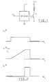
- FIG. 1 A driving system for an inductor is depicted in Fig. 1.
- the inductor L is connected between a supply node Vs and a transistor T 1 that acts as a switch, driven by a drive circuit (DRIVE) to an input of which a signal V IN is applied.
- DRIVE drive circuit
- the power stage normally comprises a circuit for limiting the maximum current in order to avoid destruction of the transistor, therefore in the diagram of Fig. 2, the current is limited to a maximum value I max .
- the transistor T 1 must be turned-off always at the same level of energy stored in the inductor, it is necessary to produce a signal when the current I reaches a preset level I D , in order to maximize the energy stored in the inductor at the end of each charging phase, that is when T 1 turns off. This is often required, for example, in electronic sparkplug driving, where it is also necessary that the level I D at which the turning off occurs be very close to the maximum limit current I max .
- a second diagnostic comparator (DIAGNOSTIC) A2 is employed.
- E 1 must also be greater than E 2 but must have a value very close thereto.
- the absolute values of E 1 as well as of E 2 should on the other hand be as low as possible, because to them corresponds a voltage drop on R s due to the current I c . Such a voltage drop is in series with the saturation voltage of the transistor and causes power dissipation, therefore the voltage on R s and therefore also E 1 and E 2 should not be greater than few 10mV. This means that if a diagnostic signal, for example for a value greater than 90% of the limit current I max , is required; E 2 >0.9*E 1 must be verified.
- Fig. 3 The known arrangement of Fig. 3 is critical, because the voltage difference on R s at which the operational amplifiers A 1 and A 2 must react is very small (in the order of millivolts) and is comparable in terms of order of magnitude with the voltage offset of the comparators that are employed. This may determine a non-negligeable imprecision in the signalling of the reaching by the current I c of the diagnostic level I D . Eventually, if the offset of the differential amplifier A 2 become greater in absolute value than the voltage difference E 1 - E 2 , the system will not produce the required diagnostic signal, with serious consequence on the functioning of the system.
- a main objective of the present invention is to provide a system for generating a diagnostic signal, indicative of the reaching by the current flowing through a power transistor of a preset level, the precision of which be substantially insensitive to the input offset of the respective detecting circuits.
- a further aim of the invention is to simplify the known circuit by employing a single monitoring comparator in order to eliminate the imprecision deriving from different characteristics of equivalent input offset of distinct monitoring comparators.
- the circuit employs a single detecting differential amplifier, capable of producing a signal the level of which is a function of the difference between a reference voltage and a voltage present across a sensing resistance of the current flowing through the power transistor.
- the signal produced by the differential amplifier is conventionally employed for driving a transistor that is functionally connected so as to subtract part of a driving current that is delivered toward the power transistor by a conventional drive circuit.
- the signal present across said second transistor is employed for producing the desired diagnostic signal by employing a threshold circuit.
- the second transistor driven in a current mirror relationship with the first current limiting transistor, reaches a state of saturation before the first transistor and therefore determines the triggering of a threshold circuit that generates the diagnostic signal upon the reaching of a current level I D, positively lower by a pre-established quantity than the limit current value I max .
- the current forced through the second transistor Is a mirrored current that may have a given ratio with a driving current that is delivered toward the power transistor.
- the ratio between I D and I max no longer depends on the input equivalent offset of the comparator, as in the circuits of the prior art, because the respective circuits that determine: one, the limit value of the current through the output power transistor, and the other, the generation of a diagnostic signal upon the reaching of a certain level I D by the current, are both driven by the same signal produced by the comparator. Therefore, the circuit permits to fix said ratio even very close to unity, though ensuring a correct operation of the circuit also in presence of disturbances. In practice, the invention allows to maximize the energy handled by the power transistor, while retaining a high degree of safety and realiability.
- the invention contemplates the use of a single comparator, which may be constituted by a differential amplifier A (comparator) capable of generating a signal in function of the difference between a reference voltage E 1 and the voltage present across a sensing resistance R s , through which the current I c flowing in the power transistor T 1 (and in the load L) flows.
- a differential amplifier A comparative amplifier
- the signal produced by the comparator A drives two circuits.
- the first circuit (LIMITATOR) produces a limiting signal of the maximum current that may flow through the power transistor T 1 , which acts on the drive circuit (DRIVE) that delivers a driving current to the power transistor T 1 .
- the second circuit (DIAGNOSTIC) is a circuit capable of producing a diagnostic signal V D upon the reaching by part of the current I c of a value I D that is lower by a pre-established amount than the limiting value I max of the current I c , as established by the LIMITATOR circuit.
- FIG. 5 A preferred embodiment of the circuit of the invention is shown in Fig. 5.
- the circuit operates in the following manner.
- V IN is commanded high
- the control circuit DRIVE closes the switch M and a current I G flows in T 2 .
- T 4 and T 5 both connected in a current mirror configuration with the transistor T 2 , are turned-on and generate currents, the value of which will depend on the respective ratio of emitter area with T 2 .
- I max E 1 /R S
- the differential amplifier A is activated and through its output starts to deliver current to the bases of the transistors T 6 and T 7 .
- I B I c /h FE (T 1 )
- the signal V D is generated upon the turning-on of T 3 , which is determined by the signal present substantially across the transistor T 6 .
- I F I max /[h FE (T 1 )*h FE (T 9 )]. In fact, I F depends on the current gains of T 1 and T 9 , which may vary with the temperature and/or be subject to a process "spread".
- an additional circuit composed of the transistors T 8 and T 10 , may be introduced, as shown in the embodiment of Fig. 5.
- the function of the additional circuit is the following.
- I 8 I c h FE (T 1 ) * (1 + A 10 /A 8 + A 9 /A 8 )
- the term I 8 is present both in the expression (1) and in the expression (2) which, if combined with the equation (3), show that the condition of generation of a diagnostic signal is practically independent on the current gain of the power transistor T 1 .
Landscapes
- Engineering & Computer Science (AREA)
- Chemical & Material Sciences (AREA)
- Combustion & Propulsion (AREA)
- Mechanical Engineering (AREA)
- General Engineering & Computer Science (AREA)
- Amplifiers (AREA)
- Electronic Switches (AREA)
- Testing Of Individual Semiconductor Devices (AREA)
- Measurement Of Current Or Voltage (AREA)
Description
IF = I10; I9 = {A9/A10} * I10; I8 = {A8/A10} * I10
where A8, A9 and A10 are the respective emitter areas of the transistors.
I6 > I4 - I8; while I7 = I5 = IF; but IF = I10 and I8 = {A8/A10} * I10
from where, by assuming for example A8 = A10, the following relationships are derived:
Claims (5)
- A circuit for limiting the maximum current (Imax) through a power transistor (T1) and for generating a diagnostic signal (VD), indicative of the reaching by the current (Ic) through said power transistor T1 of a preset level (ID), lower than a maximum current level (Imax), comprising a differential amplifier (A) having an output on which is generated a signal whose amplitude is a function of the difference between a reference voltage (E1) and a voltage present across a sensing resistance (Rs) through which said current (Ic) flows functionally coupled to respective inputs of said amplifier and at least a first transistor (T7) having a control terminal coupled to the output of said amplifier (A) and functionally connected to subtract by sinking it to a common ground node of the circuit a portion (I7) of a driving current (I5) of said power transistor (T1) produced by a driving circuit for limiting said current (Ic), characterized by comprisingat least a second transistor (T6) having a control terminal coupled to the output of said amplifier (A);current operating means (T4) forcing through said second transistor (T6) a current (I4) lower than said current (I7) subtracted by said first transistor (T7);a threshold circuit (T3, R1), sensing the voltage present across said second transistor (T6), and producing said diagnostic signal (VD).
- The circuit as defined in claim 1, characterized in that said current operating means are in the form of a current mirror circuit (T2, T4, T5), a first output branch thereof (T4) forcing said current (I4) through said second transistor (T6), and a second output branch thereof (T5) forcing said drive current (I5) to a control node of said power transistor (T1).
- A circuit according to claim 2, wherein the transistor (T4) of said first branch of the current mirror that forces said current (I4) through said second transistor (T6) has a smaller emitter area than the transistor (T5) of said second branch of the current mirror that forces said drive current (I5).
- A circuit according to claim 3, wherein said power transistor (T1) is driven through a stage composed of a fifth transistor (T9), driven by a current equivalent to the drive current (I5) forced by said transistor of said second branch of the current mirror (T2,T4,T5) less said current portion (I7), subtracted by said first transistor (T7).
- The circuit according to claim 4, characterized by comprising a sixth transistor (T8), that forms together with said fifth transistor (T9), and a seventh, diode-configured, transistor (T10), a second current mirror with said sixth transistor (T8) absorbing current from a driving node of said threshold circuit (T3, R1); the ratio among the respective emitter areas of said fifth, sixth and seventh transistors (T9, T8, T10) being such as to render the triggering condition of said threshold circuit (T3, R1) independent from variation of the current gain of the power transistor (T1).
Priority Applications (4)
| Application Number | Priority Date | Filing Date | Title |
|---|---|---|---|
| EP93830473A EP0655553B1 (en) | 1993-11-29 | 1993-11-29 | Generation of a diagnostic signal when the current through a power transistor reaches a level close to a limit current |
| DE69316627T DE69316627T2 (en) | 1993-11-29 | 1993-11-29 | Generation of a diagnostic signal when a limit current is reached by a power transistor |
| US08/272,786 US5617046A (en) | 1993-11-29 | 1994-07-08 | Generation of a diagnostic signal when the current through a power transistor reaches a level close to a limit current |
| JP6319043A JPH07260838A (en) | 1993-11-29 | 1994-11-29 | Method and circuit for generating a diagnostic signal when the current through a power transistor reaches a level close to a limiting current |
Applications Claiming Priority (1)
| Application Number | Priority Date | Filing Date | Title |
|---|---|---|---|
| EP93830473A EP0655553B1 (en) | 1993-11-29 | 1993-11-29 | Generation of a diagnostic signal when the current through a power transistor reaches a level close to a limit current |
Publications (2)
| Publication Number | Publication Date |
|---|---|
| EP0655553A1 EP0655553A1 (en) | 1995-05-31 |
| EP0655553B1 true EP0655553B1 (en) | 1998-01-21 |
Family
ID=8215254
Family Applications (1)
| Application Number | Title | Priority Date | Filing Date |
|---|---|---|---|
| EP93830473A Expired - Lifetime EP0655553B1 (en) | 1993-11-29 | 1993-11-29 | Generation of a diagnostic signal when the current through a power transistor reaches a level close to a limit current |
Country Status (4)
| Country | Link |
|---|---|
| US (1) | US5617046A (en) |
| EP (1) | EP0655553B1 (en) |
| JP (1) | JPH07260838A (en) |
| DE (1) | DE69316627T2 (en) |
Families Citing this family (3)
| Publication number | Priority date | Publication date | Assignee | Title |
|---|---|---|---|---|
| US5856760A (en) * | 1996-11-07 | 1999-01-05 | Raytheon Company | Overdrive protection clamp scheme for feedback amplifiers |
| US6127882A (en) * | 1999-02-23 | 2000-10-03 | Maxim Integrated Products, Inc. | Current monitors with independently adjustable dual level current thresholds |
| US6369621B1 (en) * | 2001-03-29 | 2002-04-09 | Texas Instruments Incorporated | Voltage/current mode TIA/EIA-644 compliant fast LVDS driver with output current limit |
Family Cites Families (10)
| Publication number | Priority date | Publication date | Assignee | Title |
|---|---|---|---|---|
| US957008A (en) * | 1909-05-17 | 1910-05-03 | Landers Frary And Clark | Safety-razor. |
| UST957008I4 (en) * | 1976-04-12 | 1977-04-05 | Rca Corporation | Switching circuit with accurate current threshold |
| DE2952462C2 (en) * | 1979-12-27 | 1982-01-21 | Siemens AG, 1000 Berlin und 8000 München | Monitoring device for identifying the operating status of a consumer |
| DE3533523A1 (en) * | 1984-09-22 | 1986-04-17 | Sharp K.K., Osaka | FAILURE DETECTOR |
| IT1208855B (en) * | 1987-03-02 | 1989-07-10 | Marelli Autronica | VARIABLE SPARK ENERGY IGNITION SYSTEM FOR INTERNAL COMBUSTION ENGINES PARTICULARLY FOR MOTOR VEHICLES |
| US4914357A (en) * | 1988-03-23 | 1990-04-03 | Unitrode Corporation | Temperature compensated foldback current limiting |
| US4914317A (en) * | 1988-12-12 | 1990-04-03 | Texas Instruments Incorporated | Adjustable current limiting scheme for driver circuits |
| IT1248607B (en) * | 1991-05-21 | 1995-01-19 | Cons Ric Microelettronica | PILOT CIRCUIT OF A POWER TRANSISTOR WITH A BASIC CURRENT FUNCTION OF THE COLLECTOR FUNCTION |
| US5168209A (en) * | 1991-06-14 | 1992-12-01 | Texas Instruments Incorporated | AC stabilization using a low frequency zero created by a small internal capacitor, such as in a low drop-out voltage regulator |
| JPH06196957A (en) * | 1992-12-25 | 1994-07-15 | Mitsubishi Electric Corp | Signal processing circuit |
-
1993
- 1993-11-29 EP EP93830473A patent/EP0655553B1/en not_active Expired - Lifetime
- 1993-11-29 DE DE69316627T patent/DE69316627T2/en not_active Expired - Fee Related
-
1994
- 1994-07-08 US US08/272,786 patent/US5617046A/en not_active Expired - Lifetime
- 1994-11-29 JP JP6319043A patent/JPH07260838A/en active Pending
Also Published As
| Publication number | Publication date |
|---|---|
| JPH07260838A (en) | 1995-10-13 |
| DE69316627T2 (en) | 1998-05-07 |
| US5617046A (en) | 1997-04-01 |
| EP0655553A1 (en) | 1995-05-31 |
| DE69316627D1 (en) | 1998-02-26 |
Similar Documents
| Publication | Publication Date | Title |
|---|---|---|
| EP0316781B1 (en) | Dual input low dropout voltage regulator | |
| US5113158A (en) | Pulse width modulation circuit | |
| US4291259A (en) | Control apparatus for controlling transistor chopper for use in current supply for electric motor | |
| US3989992A (en) | Pulse width modulated control system | |
| US6507227B2 (en) | Device and method for monitoring current delivered to a load | |
| US3426290A (en) | Amplifier having series regulated voltage supply | |
| US4902957A (en) | DC/DC converter | |
| EP0512920B1 (en) | Voltage detection circuit with common-base configured transistor | |
| US9998107B2 (en) | Current-controlled active diode | |
| US4792745A (en) | Dual transistor output stage | |
| US4492213A (en) | Ignition system for internal combustion engines | |
| US6218816B1 (en) | Power supply with control circuit for short circuit detection and excess current protection | |
| US4999566A (en) | Current converter comprising current responsive, self oscillating, switching regulator | |
| US5617046A (en) | Generation of a diagnostic signal when the current through a power transistor reaches a level close to a limit current | |
| US5838524A (en) | Current limit circuit for inhibiting voltage overshoot | |
| US4513241A (en) | Foldback current limiting driver | |
| US4789818A (en) | DC voltage converter | |
| US5105145A (en) | Voltage control circuit | |
| US4527104A (en) | Speed control apparatus for d.c. motor | |
| US4649465A (en) | Voltage stabilizer for a high-voltage generating circuit | |
| US5801352A (en) | Power supply unit for discharge apparatus which prevents excessive electrode wear | |
| US4931750A (en) | Voltage controlled oscillator | |
| US7159583B2 (en) | Technique for drive current stabilization of an automotive ignition system | |
| US6552518B2 (en) | Current generator with thermal protection | |
| US4347467A (en) | Control circuit for a D.C. motor |
Legal Events
| Date | Code | Title | Description |
|---|---|---|---|
| PUAI | Public reference made under article 153(3) epc to a published international application that has entered the european phase |
Free format text: ORIGINAL CODE: 0009012 |
|
| AK | Designated contracting states |
Kind code of ref document: A1 Designated state(s): DE FR GB IT |
|
| 17P | Request for examination filed |
Effective date: 19951116 |
|
| 17Q | First examination report despatched |
Effective date: 19960605 |
|
| GRAG | Despatch of communication of intention to grant |
Free format text: ORIGINAL CODE: EPIDOS AGRA |
|
| GRAH | Despatch of communication of intention to grant a patent |
Free format text: ORIGINAL CODE: EPIDOS IGRA |
|
| GRAH | Despatch of communication of intention to grant a patent |
Free format text: ORIGINAL CODE: EPIDOS IGRA |
|
| GRAA | (expected) grant |
Free format text: ORIGINAL CODE: 0009210 |
|
| AK | Designated contracting states |
Kind code of ref document: B1 Designated state(s): DE FR GB IT |
|
| REF | Corresponds to: |
Ref document number: 69316627 Country of ref document: DE Date of ref document: 19980226 |
|
| ITF | It: translation for a ep patent filed | ||
| ET | Fr: translation filed | ||
| RAP4 | Party data changed (patent owner data changed or rights of a patent transferred) |
Owner name: CONSORZIO PER LA RICERCA SULLA MICROELETTRONICA N Owner name: STMICROELECTRONICS S.R.L. |
|
| PLBE | No opposition filed within time limit |
Free format text: ORIGINAL CODE: 0009261 |
|
| STAA | Information on the status of an ep patent application or granted ep patent |
Free format text: STATUS: NO OPPOSITION FILED WITHIN TIME LIMIT |
|
| 26N | No opposition filed | ||
| PGFP | Annual fee paid to national office [announced via postgrant information from national office to epo] |
Ref country code: FR Payment date: 20011113 Year of fee payment: 9 |
|
| PGFP | Annual fee paid to national office [announced via postgrant information from national office to epo] |
Ref country code: GB Payment date: 20011128 Year of fee payment: 9 |
|
| PGFP | Annual fee paid to national office [announced via postgrant information from national office to epo] |
Ref country code: DE Payment date: 20011217 Year of fee payment: 9 |
|
| REG | Reference to a national code |
Ref country code: GB Ref legal event code: IF02 |
|
| PG25 | Lapsed in a contracting state [announced via postgrant information from national office to epo] |
Ref country code: GB Free format text: LAPSE BECAUSE OF NON-PAYMENT OF DUE FEES Effective date: 20021129 |
|
| PG25 | Lapsed in a contracting state [announced via postgrant information from national office to epo] |
Ref country code: DE Free format text: LAPSE BECAUSE OF NON-PAYMENT OF DUE FEES Effective date: 20030603 |
|
| GBPC | Gb: european patent ceased through non-payment of renewal fee | ||
| PG25 | Lapsed in a contracting state [announced via postgrant information from national office to epo] |
Ref country code: FR Free format text: LAPSE BECAUSE OF NON-PAYMENT OF DUE FEES Effective date: 20030731 |
|
| REG | Reference to a national code |
Ref country code: FR Ref legal event code: ST |
|
| PG25 | Lapsed in a contracting state [announced via postgrant information from national office to epo] |
Ref country code: IT Free format text: LAPSE BECAUSE OF NON-PAYMENT OF DUE FEES;WARNING: LAPSES OF ITALIAN PATENTS WITH EFFECTIVE DATE BEFORE 2007 MAY HAVE OCCURRED AT ANY TIME BEFORE 2007. THE CORRECT EFFECTIVE DATE MAY BE DIFFERENT FROM THE ONE RECORDED. Effective date: 20051129 |