EP0652440B1 - Improved acceleration sensor apparatus and method for making same - Google Patents
Improved acceleration sensor apparatus and method for making same Download PDFInfo
- Publication number
- EP0652440B1 EP0652440B1 EP94307880A EP94307880A EP0652440B1 EP 0652440 B1 EP0652440 B1 EP 0652440B1 EP 94307880 A EP94307880 A EP 94307880A EP 94307880 A EP94307880 A EP 94307880A EP 0652440 B1 EP0652440 B1 EP 0652440B1
- Authority
- EP
- European Patent Office
- Prior art keywords
- mounting element
- bore
- pin
- substrate
- acceleration sensor
- Prior art date
- Legal status (The legal status is an assumption and is not a legal conclusion. Google has not performed a legal analysis and makes no representation as to the accuracy of the status listed.)
- Expired - Lifetime
Links
- 230000001133 acceleration Effects 0.000 title claims description 25
- 238000000034 method Methods 0.000 title description 8
- 239000000758 substrate Substances 0.000 claims description 55
- 229910052751 metal Inorganic materials 0.000 claims description 12
- 239000002184 metal Substances 0.000 claims description 12
- 238000003780 insertion Methods 0.000 claims description 8
- 230000037431 insertion Effects 0.000 claims description 8
- PNEYBMLMFCGWSK-UHFFFAOYSA-N Alumina Chemical compound [O-2].[O-2].[O-2].[Al+3].[Al+3] PNEYBMLMFCGWSK-UHFFFAOYSA-N 0.000 claims description 5
- 230000004044 response Effects 0.000 claims description 5
- 239000007787 solid Substances 0.000 claims description 5
- XEEYBQQBJWHFJM-UHFFFAOYSA-N Iron Chemical compound [Fe] XEEYBQQBJWHFJM-UHFFFAOYSA-N 0.000 claims description 4
- PXHVJJICTQNCMI-UHFFFAOYSA-N Nickel Chemical compound [Ni] PXHVJJICTQNCMI-UHFFFAOYSA-N 0.000 claims description 4
- 239000003990 capacitor Substances 0.000 claims description 4
- 239000000203 mixture Substances 0.000 claims description 3
- 230000002093 peripheral effect Effects 0.000 claims description 3
- 229910052742 iron Inorganic materials 0.000 claims description 2
- 229910052759 nickel Inorganic materials 0.000 claims description 2
- 239000000463 material Substances 0.000 description 19
- 230000035882 stress Effects 0.000 description 11
- 239000011248 coating agent Substances 0.000 description 9
- 238000000576 coating method Methods 0.000 description 9
- 238000003466 welding Methods 0.000 description 9
- 238000002955 isolation Methods 0.000 description 7
- 229910045601 alloy Inorganic materials 0.000 description 6
- 239000000956 alloy Substances 0.000 description 6
- 125000006850 spacer group Chemical group 0.000 description 6
- 238000005452 bending Methods 0.000 description 5
- 238000007650 screen-printing Methods 0.000 description 5
- 229910000679 solder Inorganic materials 0.000 description 4
- 230000004308 accommodation Effects 0.000 description 3
- 230000008901 benefit Effects 0.000 description 3
- 230000035939 shock Effects 0.000 description 3
- 239000000853 adhesive Substances 0.000 description 2
- 230000001070 adhesive effect Effects 0.000 description 2
- 230000005540 biological transmission Effects 0.000 description 2
- 238000013016 damping Methods 0.000 description 2
- PCHJSUWPFVWCPO-UHFFFAOYSA-N gold Chemical compound [Au] PCHJSUWPFVWCPO-UHFFFAOYSA-N 0.000 description 2
- 239000010931 gold Substances 0.000 description 2
- 229910052737 gold Inorganic materials 0.000 description 2
- 230000001939 inductive effect Effects 0.000 description 2
- 239000007788 liquid Substances 0.000 description 2
- 238000012986 modification Methods 0.000 description 2
- 230000004048 modification Effects 0.000 description 2
- 230000008569 process Effects 0.000 description 2
- 230000008646 thermal stress Effects 0.000 description 2
- 229910018404 Al2 O3 Inorganic materials 0.000 description 1
- 239000004593 Epoxy Substances 0.000 description 1
- 230000002411 adverse Effects 0.000 description 1
- 239000000919 ceramic Substances 0.000 description 1
- 229910052593 corundum Inorganic materials 0.000 description 1
- 238000005336 cracking Methods 0.000 description 1
- 230000003292 diminished effect Effects 0.000 description 1
- 230000000694 effects Effects 0.000 description 1
- 239000012777 electrically insulating material Substances 0.000 description 1
- 230000002708 enhancing effect Effects 0.000 description 1
- 229920006332 epoxy adhesive Polymers 0.000 description 1
- 230000004907 flux Effects 0.000 description 1
- -1 for example Substances 0.000 description 1
- 239000011521 glass Substances 0.000 description 1
- 238000000227 grinding Methods 0.000 description 1
- 238000004519 manufacturing process Methods 0.000 description 1
- 230000007246 mechanism Effects 0.000 description 1
- TWNQGVIAIRXVLR-UHFFFAOYSA-N oxo(oxoalumanyloxy)alumane Chemical compound O=[Al]O[Al]=O TWNQGVIAIRXVLR-UHFFFAOYSA-N 0.000 description 1
- 229920003223 poly(pyromellitimide-1,4-diphenyl ether) Polymers 0.000 description 1
- 238000002360 preparation method Methods 0.000 description 1
- 238000012545 processing Methods 0.000 description 1
- 230000001737 promoting effect Effects 0.000 description 1
- 238000012216 screening Methods 0.000 description 1
- 238000012360 testing method Methods 0.000 description 1
- 230000007704 transition Effects 0.000 description 1
- 229910001845 yogo sapphire Inorganic materials 0.000 description 1
Images




Classifications
-
- G—PHYSICS
- G01—MEASURING; TESTING
- G01P—MEASURING LINEAR OR ANGULAR SPEED, ACCELERATION, DECELERATION, OR SHOCK; INDICATING PRESENCE, ABSENCE, OR DIRECTION, OF MOVEMENT
- G01P1/00—Details of instruments
- G01P1/02—Housings
- G01P1/023—Housings for acceleration measuring devices
-
- G—PHYSICS
- G01—MEASURING; TESTING
- G01P—MEASURING LINEAR OR ANGULAR SPEED, ACCELERATION, DECELERATION, OR SHOCK; INDICATING PRESENCE, ABSENCE, OR DIRECTION, OF MOVEMENT
- G01P15/00—Measuring acceleration; Measuring deceleration; Measuring shock, i.e. sudden change of acceleration
- G01P15/02—Measuring acceleration; Measuring deceleration; Measuring shock, i.e. sudden change of acceleration by making use of inertia forces using solid seismic masses
- G01P15/08—Measuring acceleration; Measuring deceleration; Measuring shock, i.e. sudden change of acceleration by making use of inertia forces using solid seismic masses with conversion into electric or magnetic values
- G01P15/125—Measuring acceleration; Measuring deceleration; Measuring shock, i.e. sudden change of acceleration by making use of inertia forces using solid seismic masses with conversion into electric or magnetic values by capacitive pick-up
-
- G—PHYSICS
- G01—MEASURING; TESTING
- G01P—MEASURING LINEAR OR ANGULAR SPEED, ACCELERATION, DECELERATION, OR SHOCK; INDICATING PRESENCE, ABSENCE, OR DIRECTION, OF MOVEMENT
- G01P15/00—Measuring acceleration; Measuring deceleration; Measuring shock, i.e. sudden change of acceleration
- G01P15/02—Measuring acceleration; Measuring deceleration; Measuring shock, i.e. sudden change of acceleration by making use of inertia forces using solid seismic masses
- G01P15/08—Measuring acceleration; Measuring deceleration; Measuring shock, i.e. sudden change of acceleration by making use of inertia forces using solid seismic masses with conversion into electric or magnetic values
- G01P2015/0805—Measuring acceleration; Measuring deceleration; Measuring shock, i.e. sudden change of acceleration by making use of inertia forces using solid seismic masses with conversion into electric or magnetic values being provided with a particular type of spring-mass-system for defining the displacement of a seismic mass due to an external acceleration
- G01P2015/0822—Measuring acceleration; Measuring deceleration; Measuring shock, i.e. sudden change of acceleration by making use of inertia forces using solid seismic masses with conversion into electric or magnetic values being provided with a particular type of spring-mass-system for defining the displacement of a seismic mass due to an external acceleration for defining out-of-plane movement of the mass
- G01P2015/0825—Measuring acceleration; Measuring deceleration; Measuring shock, i.e. sudden change of acceleration by making use of inertia forces using solid seismic masses with conversion into electric or magnetic values being provided with a particular type of spring-mass-system for defining the displacement of a seismic mass due to an external acceleration for defining out-of-plane movement of the mass for one single degree of freedom of movement of the mass
- G01P2015/0828—Measuring acceleration; Measuring deceleration; Measuring shock, i.e. sudden change of acceleration by making use of inertia forces using solid seismic masses with conversion into electric or magnetic values being provided with a particular type of spring-mass-system for defining the displacement of a seismic mass due to an external acceleration for defining out-of-plane movement of the mass for one single degree of freedom of movement of the mass the mass being of the paddle type being suspended at one of its longitudinal ends
-
- Y—GENERAL TAGGING OF NEW TECHNOLOGICAL DEVELOPMENTS; GENERAL TAGGING OF CROSS-SECTIONAL TECHNOLOGIES SPANNING OVER SEVERAL SECTIONS OF THE IPC; TECHNICAL SUBJECTS COVERED BY FORMER USPC CROSS-REFERENCE ART COLLECTIONS [XRACs] AND DIGESTS
- Y10—TECHNICAL SUBJECTS COVERED BY FORMER USPC
- Y10T—TECHNICAL SUBJECTS COVERED BY FORMER US CLASSIFICATION
- Y10T29/00—Metal working
- Y10T29/43—Electric condenser making
-
- Y—GENERAL TAGGING OF NEW TECHNOLOGICAL DEVELOPMENTS; GENERAL TAGGING OF CROSS-SECTIONAL TECHNOLOGIES SPANNING OVER SEVERAL SECTIONS OF THE IPC; TECHNICAL SUBJECTS COVERED BY FORMER USPC CROSS-REFERENCE ART COLLECTIONS [XRACs] AND DIGESTS
- Y10—TECHNICAL SUBJECTS COVERED BY FORMER USPC
- Y10T—TECHNICAL SUBJECTS COVERED BY FORMER US CLASSIFICATION
- Y10T29/00—Metal working
- Y10T29/49—Method of mechanical manufacture
- Y10T29/49002—Electrical device making
- Y10T29/49117—Conductor or circuit manufacturing
- Y10T29/49124—On flat or curved insulated base, e.g., printed circuit, etc.
- Y10T29/4913—Assembling to base an electrical component, e.g., capacitor, etc.
- Y10T29/49139—Assembling to base an electrical component, e.g., capacitor, etc. by inserting component lead or terminal into base aperture
Definitions
- This invention relates generally to condition sensors and more particularly to accelerometers having mechanically movable means responsive to acceleration for providing a corresponding electrical signal.
- Condition sensors such as capacitive accelerometers and the like of various types as shown in U.S. Patent Nos. 4,483,194 to Rudolph; 4,435,737 to Colton; Reissue 31,549 to Block and 3,240,073 to Pitzer are commonly used or proposed for use in aircraft and vehicular applications and the like where the sensors are likely to be subjected to shock, vibration and severe temperature changes but where it would be desirable for the sensors to be inexpensive and to display reliable and accurate performance characteristics over a long service life.
- many such sensors have limited performance capability or are manufactured at excessive cost. It would be desirable if such sensors could be provided with improved reliability in performance and could be made at reduced cost to find wider application.
- EP 0 491 506 discloses several capacitive accelerometer devices, in which a plate is mounted on but spaced from a substrate.
- the plate comprises an attachment portion which is attached to the substrate, a source plate portion, the distance of which from the substrate varies in response to acceleration, and a beam portion connecting the attachment and source plate portions.
- a detect plate is disposed on the surface of the substrate opposite the source plate portion and the capacitance between those two is measured to determine the acceleration of the device.
- the spacing between the plate and the substrate is set by a flat spacer or shim disposed between the plate and the substrate and the plate, spacer and substrate are held together with adhesive.
- the plate, spacer, and substrate are riveted together.
- the attachment plate portion is thicker than the rest of the plate and so the plate has an integral spacer.
- a shim adds, however, an additional part and process step which adds to the cost of the device as well. Further, when using a shim it is difficult to obtain close dimensional control from device to device. Use of a metal plate having a reduced thickness portion results in a more expensive blade member and one for which it is difficult to provide a properly balanced and mounted source plate portion.
- EP 0 542 436 discloses similar accelerometer devices to those of EP 0 491 506.
- the attachment portion of the plate is fixed to the substrate with solder, the detect plate being located in a hollow in the substrate. Riveting and epoxy adhesive are mentioned as alternative methods of fixing.
- the spacing between the plate and the substrate is set by glass rods used as spacers between them, the assembly being held together with conductive adhesive.
- solder as a means of attachment involves a relatively time-consuming reflow process and requires flux cleansing.
- solder creep there is a tendency for elements connected by solder to move slightly over time due to so-called solder creep thereby adversely affecting calibration of the device.
- an acceleration sensor comprising
- a base having at least the top surface of electrically insulating material is provided with an electrically conductive detect plate on a top surface thereof and at least one bore between top and bottom surfaces.
- An electrically conductive metal plate or blade is formed having an attachment portion, a source plate portion and an integral beam means connecting the attachment portion to the source plate portion.
- the attachment portion is fixedly attached, as by welding, to the end of an electrically conductive element such as a solid or hollow pin inserted into the bore with the source plate portion spaced a selected distance from the detect plate and with the element in electrical engagement with a conductive path which extends from the top surface of the substrate into the bore.
- the axial position of the pin may be adjusted to provide a selected capacitance level between the detect plate and the source plate portion.
- the conductive path is formed by screen printing on the top surface and drawing the liquid coating material by means of a vacuum through an annular space defined between the wall of the bore and an insert placed in the bore during the coating step.
- the bore is specially formed with a flow inducing entrance, a burr accommodation section and a flow preventing exit.
- the pin is knurled along at least a portion of its length while in another embodiment the pin is formed with a plurality of longitudinally extending ribs having an outer surface forming arcs of a circle having a diameter which provides an interference fit in the bore.
- the pin is tubular with a closed end formed into a weld projection surface.
- the bore is formed with a plurality of splines or other inwardly projecting surface portions and the pin is formed with a conventional cylindrical wall surface.
- a pair of bores are provided in the base and a pair of pins are attached to the attachment portion and inserted in respective bores to prevent any possible rotational movement of the pins.
- the pin(s) and conductive metal plate may both be formed of the same material, for example, alloy 42 when the substrate is formed of Al 2 O 3 ceramic to closely match the thermal coefficient of expansion of the substrate.
- the attachment portion of the metal blade member is disposed at one end portion of the blade while in another embodiment the attachment portion is disposed in the center of the blade member to provide a center of mass of the blade member in alignment with the location of attachment.
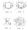
- an acceleration sensor 10 made in accordance with the invention, includes a housing 12 having suitable mounting tabs 14 for attachment to a body, such as a vehicle, the acceleration of which is desired to be monitored.
- a substrate 16, Fig. 4 formed of suitable material such as electrically insulative aluminum oxide, Al 2 O 3 , is provided with slots 18 adapted to receive mounting posts 20 in a recess 22 of base 12. It will be understood that the substrate could be composed of various materials such as metal, for example, having an electrically insulative top surface, if desired.
- Substrate 16 is provided with an electrically conductive detect plate 24 on a top surface 26 thereof. Plate 24 can be placed on the substrate in any suitable manner, as by screen printing.
- Associated circuit paths 28 a , 28 b , 28 c are also formed on surface 26 in a similar manner.
- a bore 32 is formed extending through the substrate 16 at source plate mounting portion 28c and is provided with a shallow recess 32 a (Fig. 5) on top surface 26 and a relatively larger well recess 32 b on bottom side 34 surrounding bore 32.
- a mounting element in the form of a pin 36 formed of material having a coefficient of thermal expansion closely matching that of substrate 16, is received in bore 32.
- pin 36 can be formed of Alloy 42, an alloy having a nominal composition by weight of 42 percent nickel and the balance iron.
- Both Alloy 42 and 94 percent alumina have coefficients of thermal expansion approximately 6.0 x 10 -6 cm/cm/°C in the temperature range from 25° to 100°C and comparable expansion properties over the range -40°C to 125°C.
- Pin 36 is formed with a knurled surface portion 36 a which extends around its periphery for a selected longitudinal portion of its length to provide an interference fit in bore 32.
- pin 36 For a bore in the order of .094/.096 inches (2.39/2.44 mm) the diameter of pin 36 can be on the order of .099/.097 inches (2.51/2.46 mm) so that a force between approximately 10 and 200 pounds (44 and 890 N) is required for inserting the pin into the bore without cracking the substrate.
- Pin 36 is formed with a curved end portion 36 b on either end to serve as a weld projection.
- At least circuit path 28 c is formed of metallo-organic gold in order to provide a sub-micron surface conductive path on the wall defining bore 32 which will not be wiped off by pin 36 when it is inserted in bore 32.
- recess 32a is formed in top surface 26 to form a flow inducing surface.
- a frusto-conical ramp having a shallow angle ⁇ , for example, 13° relative to surface 26 has been found to be suitable for promoting flow of coating material into the bore.
- Ramp 32 a blends in with a radius 33 of approximately .025 inches (0.64 mm) at approximately .002 inches (0.05 mm) below top surface 26 formed at the entrance of burr accommodation section 33 a .
- This provides adequate material above the radius so that grinding of the top surface to provide a smooth flat surface will not affect the radius and there will be a smooth, gradual curved surface on which the liquid coating material can flow during the screening process.
- Intermediate burr accommodation section 33 a preferably is used to provide sufficient space and a trap for any burr which might occur when a mounting pin is inserted into bore 32 from surface 26 thereby preventing any interference fit with the welding operation or the blade.
- a transition surface 33 b extends from section 33 a to bore 32 and is inclined relative to the longitudinal axis of bore 32 at a suitable angle, e.g., 35-45°, to ensure that coating material applied to the bore will not be interrupted.
- well recess 32 b is formed on the bottom surface 34 with a surface portion 32c which is preferably 90° or more relative to the wall defining bore 32 so that the flow of any coating material received in the bottom of the bore will be interrupted to break the conductive path and prevent any possibility of an electrical shorting path to bottom surface 34.
- Well 32 b can also conveniently receive epoxy which can be provided if desired, as an additional locking mechanism for the pin once the device has been calibrated as will be discussed infra. As seen in Fig.
- a screen printing fixture pin 32 d is preferably used when screen printing the conductive layers onto substrate 16.
- Pin 32 d has an outer distal post portion 32 e having an outer diameter selected to be slightly smaller than the diameter of bore 32 in order to define an annular opening between the pin and the wall defining bore 32 so that the coating material will flow through the annular opening in intimate contact with the wall to ensure that the entire wall surface is coated.
- Portion 32 f of pin 32 d closely fits within bore 32 and centers post 32 e within the bore while bores 32 g provide channels for applying a suitable vacuum indicated by arrow 32 i to draw the coating material down into the bore.
- a distal post portion 32 e having a diameter of approximately .082 - .088 inch (2.08 - 2.24 mm) provides a suitable annular passage between the substrate and the distal post portion 32 e of approximately .005 - .009 inch (0.13 - 0.23 mm) for use with metallo-organic gold.
- An electrically conductive blade member 40 Fig. 6, of the type disclosed in copending application, Serial No. 07/790,956 referenced supra, which may be formed of the same material as pin 36, e.g., Alloy 42, has an attachment portion 40 a which is attached to pin 36 as by resistance welding or the like on weld projection 36 b .
- Blade member 40 has integrally attached first and second beams 40 b , 40 c extending away from attachment portion 40 a on opposite sides of blade 40 to a respective distal end 40 d , 40 e .
- Third and fourth beams 40 f , 40 g extend laterally from the distal ends to a central portion 40 h attached to source plate portion 40 i which extends back toward attachment portion 40 a .
- Attachment portion 40 a is welded to pin 36 so that source plate portion 40 i is aligned over detect plate 24 as shown in Fig. 8. Welding can be effected either before or after the pin is inserted into bore 32. Once inserted, electrical continuity can be checked between pin 36 and output pad 28 d . If the pin is welded to the blade member prior to insertion into bore 32 capacitance between the detect plate and the source plate portion can be monitored by connecting them to an electrical source as denoted by arrows T1 and T2 in Fig. 4. A force is then applied through the blade member to the pin pushing the pin into the bore until a selected capacitance value is obtained.
- the pin is inserted into the bore prior to welding, this can be conveniently accomplished by inserting the pin into the bore leaving a space between the top of the pin and a plane in which the detect plate lies, i.e., the top surface of the substrate, greater than that which will provide the selected capacitance level, e.g., greater than "s" shown in Fig. 15, and then welding the blade member to the pin. The capacitance is then monitored as a force is applied through the blade member to the pin moving the pin until the selected capacitance level is obtained.
- the pin could also be inserted, prior to welding, leaving less than the space required to provide the selected capacitance level and then a force could be applied to the bottom of the pin through bore 32 pushing the pin and blade member away from the detect plate until the selected capacitance value is obtained.
- the position of the pin can be adjusted to provide the gap required to obtain the selected capacitance level resulting in virtually 100 percent yield and providing consistency from one device to another. This provides additional advantages in enhancing the frequency response or damping factor due to the consistent air gap from device to device as well as facilitating placement of stop surfaces to prevent over-travel.
- FIG. 7 A modified embodiment is shown in Fig. 7 in which the blade member mounting element takes the form of a cup-shaped hollow pin 36' in place of the solid pin 36 shown in Fig. 5.
- Hollow pin 36' again, may be formed of the same material as blade 40, e.g., .010 inch (0.25 mm) Alloy 42, and is inserted into bore 32 in substrate 16.
- Blade member 40 is placed in a recess 42 a of a suitable electrically insulating jig 42.
- a movable electrode 42 b is received in hollow pin 36' and a stationary electrode 42 c is disposed in a bore 42 d of jig 42 and in alignment with electrode 42 b for welding hollow pin 36' to blade 40.
- hollow pin 36' is formed with a radiused closed end 36 b ', as shown in Fig. 7a to serve as a weld projection.
- FIG. 9 Another modified embodiment of the invention is shown in Fig. 9 in which substrate 16' is provided with a pair of bores 32' in order to provide improved anti-rotational control of a blade member mounted on the substrate.
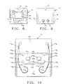
- Fig. 10 shows a preferred embodiment of a blade member having an integral source plate portion with improved thermal error characteristics. Any differences in coefficient of thermal expansion of joined ports, however small, will result in the joint being stressed when changes in temperature of joined materials occurs. The most common effect of this thermal stress is a bending of the joined material - called the bimetal affect. Blade member 44 incorporates several features which minimize the outward affects of bending caused by thermal expansion mismatch in the attached joint.
- blade member 44 is formed of material having a selected coefficient of thermal expansion relative to that of the substrate to which it is to be mounted.
- Blade member 44 has a source plate portion 44 a , the center of seismic mass, attached at each lateral side to a respective beam 44 b defined by a slot 44 c which extends the full length of blade member 44, i.e., along a y-axis.
- Each opposite end of beam 44 b is integrally attached to a respective side of a central brace portion 44 d .
- Central brace portion 44 d is attached at each side to a laterally extending, i.e., along an x-axis, slender isolation beam 44 e defined by a laterally extending slot f and a curved end portion 44 g of slot 44 c .
- Beams 44 e are in turn connected to an attachment portion 44 h through slender, laterally extending isolation beams 44 i and a counterflexing zone 44 j .
- Beams 44 i extend above and below isolation windows 44 k and are defined by slot 44 l on the top and slot 44 f on the bottom, as seen in Fig. 10.
- Isolation slots 44 m extend downwardly from slot 44 l to match end portions 44 n of slot 44 f .
- a welded attachment to a mounting member is made at attachment portion 44 h .
- Changes in temperature will result in a bending stress being applied to the weld region causing the blade member to bend or develop a curvature.
- the input to the blade member from this curvature is to impose a curved boundary condition to the blade member at the attachment area.
- the boundary condition is circular in nature and will cause bending around the x-axis and the y-axis.
- Windows 44 k cut in the attachment portion create two slender, laterally extending isolation beams 44 i that reduce the rigidity of the attachment portion.
- Beam members 44 i also twist in response to the y-direction imposed boundary condition. Isolation cuts 44 m , 44 n enhance the ability of beam members 44 i to twist.
- the counterflexing zone 44 i extends from the isolation cuts 44 m down to the curved slot 44 g . The function of the counterflexing zone is to contain remaining x-direction bending stresses to the x-direction.
- the lateral position of curve slot 44 g relative to slot 44 f is selected to define slender beams 44 e which extend laterally, generally parallel to beam 44 i to central brace portion 44 d . If curved slot 44 g were moved outward toward beams 44 b , a y-direction stress component would be generated, forcing central brace portion 44 d to tilt, changing the capacitor gap at source plate portion 44 a .
- the central brace portion 44 d is a stiff section to stop further transmission of the boundary condition stress. The end result of this arrangement of beams and holes is to allow thermal stresses generated in the weld attachment to gradually be diminished, while not changing the capacitor gap at source plate portion 44 a .
- Curved slot feature 44 g is formed with a relatively large radius to reduce notch stresses from an x-axis drop. Tapered sections 44 o and 44 p of beams 44 b are tapered to minimize the moment stress applied to the arcs where beams 44 b are connected to central brace portion 44 d . The width of slot 44 c is selected to allow counterflexing zone 44 j to act as a cross axis stop. This minimizes stresses generated in beams 44 b .
- the welded attachment area is positioned over the center of mass of the blade member to minimize torsional shear stress of the weld during a cross axis shock test.
- the size of source plate portion 44 i is selected for controlling the squeeze film damping factor. That is, if the size is too small, portion 44 i will resonate and if it is too large, it will not be sufficiently sensitive. Beams 44b are sized to provide adequate movement of the seismic mass, i.e., portion 44 i .
- the blade is chemically etched using standard integrated circuit lead frame processing to provide a stress free, flat part preferably in reel form. Mounting parts on reels reduces handling and transportation damages as well as allows for high speed automated assembly.
- a pin 36" is shown formed with a plurality of longitudinally extending ribs 36 a ", preferably having a radiused outer peripheral surface.
- the ribs can be formed by any suitable means as by stamping equally spaced flat portions 36 d " each covering 90°, for example, leaving three ribs each covering 30° and having an outer radius for each rib comparable but slightly larger than that of the pin before stamping.
- pin 36" is acceptable if it passes through a ring gap of .1015 inch (2.58 mm) and not pass a gap of .1005 inch (2.55 mm).
- acceptable insertion force can be anywhere from approximately 10 to approximately 200 pounds (44 to 890 N). More specifically, with regard to the Fig. 11 and 12 pin, an insertion force of between 50 and 100 pounds (200 and 440 N) has been found to be suitable. Ends 36b" of pin 36" are formed with a suitable radius such as .125/.280 (3.18 to 7.11 mm) to serve as a weld projection so that either end can be inserted in the bore.
- Substrate 16'' shown in Figs. 13-15 may be composed of the same material as substrate 16 discussed supra, e.g., 94 percent alumina. Bore 32'' is centrally disposed on top surface 26'' and pin 36'' may be forced into bore 32'' so that weld projection surface 36 b '' extends above the surface a selected distance "s" shown in Fig. 15. Blade member 44 is mounted on substrate 16'' by welding attachment portion 44 a to weld projection surface 36 b " with source plate portion 44 i aligned with and spaced over detect plate 24.
- blade member 44 In order to ensure the desired spacing, spacers of Kapton, or the like can be placed between blade member 44 and surface 26'' on opposite sides of attachment portion 44 a or specially machined fixtures can be employed. However, preferably, as described above with reference to blade member 40, blade member 44 may be welded to pin 36'' before or after being inserted into bore 32'' and the capacitance between source plate portion 44 a and detect plate 24 can be monitored as the pin is moved in the bore with movement being stopped at the appropriate spacing when the selected capacitance value is obtained.
- pin 36"' having a smooth cylindrical surface and to form bore 32 with a plurality of splines 32 a are spaced about the periphery and projecting into the bore so that an interference fit is formed between pin 36"' and splines 32 a as shown in Fig. 18.
Landscapes
- Physics & Mathematics (AREA)
- General Physics & Mathematics (AREA)
- Pressure Sensors (AREA)
Description
- the mounting element is electrically conductive,
- the mounting element has an end extending above the top surface of the substrate by a selected distance,
- in that the attachment portion of the blade member is fixedly and electrically attached to the end of the mounting element extending above the top surface of the substrate,
- in that said mounting element has an outer surface portion which engages said bore and requires a force of between 10 and 200 pounds (44 and 890 N) to insert the mounting element into the bore for precisely and fixedly holding the mounting element in place after insertion while still allowing for movement and adjustments of the mounting element for calibration after insertion,
- and in that one of the electrically conductive circuit paths is also electrically connected to the mounting element.
Claims (10)
- An acceleration sensor (10) comprisingcharacterised in thata substrate (16) having opposite top and bottom surfaces, at least the top surface being electrically insulative,an electrically conductive detect plate (24) mounted on the top surface of the substrate,a bore (32,32',32",32"') extending through the substrate from the top surface to the bottom surface,a mounting element (36,36',36",36"') disposed in the bore,an electrically conductive metal blade member (40,44) having an attachment portion, a source plate portion and integral resilient beam means extending between the attachment portion and the source plate portion, andelectrically conductive circuit paths (28), one of which is electrically connected to the detect plate,the source plate portion overlying the detect plate in selected spaced relation to form a capacitor and to be movable relative to the detect plate in response to an acceleration force to provide an electrical signal,the mounting element is electrically conductive,the mounting element has an end extending above the top surface of the substrate by a selected distance,in that the attachment portion of the blade member is fixedly and electrically attached to the end of the mounting element extending above the top surface of the substrate,in that said mounting element has an outer surface portion which engages said bore and requires a force of between 10 and 200 pounds (44 and 890 N) to insert the mounting element into the bore for precisely and fixedly holding the mounting element in place after insertion while still allowing for movement and adjustments of the mounting element for calibration after insertion,and in that one of the electrically conductive circuit paths (28) is also electrically connected to the mounting element.
- An acceleration sensor according to claim 1 in which the attachment portion is attached to the end of the mounting element by being welded thereto.
- An acceleration sensor according to claim 1 or claim 2 in which the attachment portion of the metal blade member is centralized relative to the plate.
- An acceleration sensor according to any one of claims 1 to 3 in which a second bore (321) is formed in the substrate between the top and bottom surfaces and a second electrically conductive mounting element is disposed in the second bore, the second mounting element having an end extending above the top surface and being fixedly attached to the attachment portion of the metal blade member.
- An acceleration sensor according to any preceding claim in which the substrate is formed of 94 per cent alumina ceramic and the mounting element and the metal blade member are each composed of metal having a nominal composition of 42 % nickel and the remainder iron.
- An acceleration sensor according to any preceding claim in which the or each mounting element is a hollow pin (36') having a closed end forming the said end extending above the top surface.
- An acceleration sensor according to any one of claims 1 to 5 in which the or each mounting element is a solid pin (36) having a knurled outer surface portion.
- An acceleration sensor according to any one of claims 1 to 5 in which the or each mounting element is a solid, generally cylindrical pin (36") having a longitudinal axis and having a plurality of longitudinally extending ribs formed on the pin.
- An acceleration sensor according to any one of claims 1 to 5 in which the or each bore (32") is formed with a plurality of spaced projections extending into the bore and extending in a direction generally parallel to the longitudinal axis of the bore and the mounting element has a generally cylindrical peripheral surface.
- An acceleration sensor according to any one of claims 1 to 5 in which the or each mounting element is a solid, generally cylindrical pin having a longitudinal axis and having three spaced, longitudinally extending ribs formed on the pin, the outer surface of each of the ribs being curved and covering in total approximately 90° around the outer peripheral surface of the pin.
Applications Claiming Priority (2)
| Application Number | Priority Date | Filing Date | Title |
|---|---|---|---|
| US148042 | 1993-11-04 | ||
| US08/148,042 US5555766A (en) | 1993-11-04 | 1993-11-04 | Acceleration sensor apparatus and method for making same |
Publications (2)
| Publication Number | Publication Date |
|---|---|
| EP0652440A1 EP0652440A1 (en) | 1995-05-10 |
| EP0652440B1 true EP0652440B1 (en) | 1998-06-03 |
Family
ID=22523983
Family Applications (1)
| Application Number | Title | Priority Date | Filing Date |
|---|---|---|---|
| EP94307880A Expired - Lifetime EP0652440B1 (en) | 1993-11-04 | 1994-10-26 | Improved acceleration sensor apparatus and method for making same |
Country Status (4)
| Country | Link |
|---|---|
| US (2) | US5555766A (en) |
| EP (1) | EP0652440B1 (en) |
| JP (1) | JP3437876B2 (en) |
| DE (1) | DE69410749T2 (en) |
Families Citing this family (16)
| Publication number | Priority date | Publication date | Assignee | Title |
|---|---|---|---|---|
| US5542296A (en) * | 1995-01-03 | 1996-08-06 | Reidemeister; Eric P. | Compact capacitive acceleration sensor |
| US5808539A (en) * | 1996-10-10 | 1998-09-15 | Texas Instruments Incorporated | Temperature responsive snap acting control assembly, device using such assembly and method for making |
| US6412165B1 (en) | 1997-08-28 | 2002-07-02 | Texas Instruments Incorporated | Temperature responsive snap acting control assembly, device using such assembly and method for making |
| US6465281B1 (en) | 2000-09-08 | 2002-10-15 | Motorola, Inc. | Method of manufacturing a semiconductor wafer level package |
| US6571628B1 (en) * | 2000-10-16 | 2003-06-03 | Institute Of Microelectronics | Z-axis accelerometer |
| EP1728055A1 (en) | 2004-03-26 | 2006-12-06 | Contitemic Microelectronic GmbH | Vehicle sensor for detecting impact sound |
| DE102004022822A1 (en) * | 2004-05-08 | 2005-12-01 | Conti Temic Microelectronic Gmbh | Motor vehicle sensor, for detecting impact sound, has measured-value sensor for detecting impact sound together with sensing elements coupled to vehicle's structure |
| DE102004022831A1 (en) * | 2004-05-08 | 2005-12-01 | Conti Temic Microelectronic Gmbh | Sensor system / trigger sensor, suitable for diagnostic / safety device, in particular for accident prevention devices in a vehicle |
| DE102004022830A1 (en) * | 2004-05-08 | 2005-12-01 | Conti Temic Microelectronic Gmbh | Sensor system/trigger sensor, suitable for diagnostic safety device, especially accident protection device for motor vehicle, has elastic coupling coating/viscoelastic coupling coating for acoustic wave coupling |
| DE102004022808A1 (en) * | 2004-05-08 | 2005-12-01 | Conti Temic Microelectronic Gmbh | Sensor system/trigger sensor suitable, for diagnostic safety device, especially accident protection device for motor vehicle, has elastic coupling coating/viscoelastic coupling coating for acoustic wave coupling |
| US20080125700A1 (en) * | 2006-11-29 | 2008-05-29 | Moberg Sheldon B | Methods and apparatuses for detecting medical device acceleration, temperature, and humidity conditions |
| WO2009094420A1 (en) * | 2008-01-22 | 2009-07-30 | Massachusetts Institute Of Technology | A flexural mechanism for passive angle alignment and locking |
| WO2010029516A1 (en) * | 2008-09-15 | 2010-03-18 | Nxp B.V. | A capacitive sensor device and a method of sensing accelerations |
| DE102012010722B4 (en) * | 2012-05-30 | 2025-07-24 | Kiekert Aktiengesellschaft | Motor vehicle door lock housing and method for its manufacture |
| JP1529010S (en) * | 2014-12-18 | 2015-07-21 | ||
| JP6545918B1 (en) * | 2019-05-22 | 2019-07-17 | Imv株式会社 | Acceleration sensor core unit, method for preventing deflection of substrate on which acceleration sensor is mounted |
Family Cites Families (10)
| Publication number | Priority date | Publication date | Assignee | Title |
|---|---|---|---|---|
| US3240073A (en) * | 1962-03-01 | 1966-03-15 | Edcliff Instr Inc | Linear accelerometer |
| FR1445571A (en) * | 1965-05-19 | 1966-07-15 | Electronic device for measuring very small displacements | |
| US4231010A (en) * | 1978-11-30 | 1980-10-28 | Texas Instruments Incorporated | Thermostatic switch employing a stud member for calibration of the switch |
| USRE31549E (en) * | 1978-12-11 | 1984-04-10 | Charles Bonnici | One-piece roof vent device and methods of constructing and utilizing same |
| CH642461A5 (en) * | 1981-07-02 | 1984-04-13 | Centre Electron Horloger | ACCELEROMETER. |
| US4435737A (en) * | 1981-12-16 | 1984-03-06 | Rockwell International Corporation | Low cost capacitive accelerometer |
| IT1223933B (en) * | 1988-11-23 | 1990-09-29 | Marelli Autronica | CAPACITIVE ACCELERATION TRANSDUCER |
| US5044202A (en) * | 1989-09-18 | 1991-09-03 | Texas Instruments Incorporated | Pressure transducer apparatus |
| US5239871A (en) * | 1990-12-17 | 1993-08-31 | Texas Instruments Incorporated | Capacitive accelerometer |
| US5345823A (en) * | 1991-11-12 | 1994-09-13 | Texas Instruments Incorporated | Accelerometer |
-
1993
- 1993-11-04 US US08/148,042 patent/US5555766A/en not_active Expired - Lifetime
-
1994
- 1994-10-26 EP EP94307880A patent/EP0652440B1/en not_active Expired - Lifetime
- 1994-10-26 DE DE69410749T patent/DE69410749T2/en not_active Expired - Lifetime
- 1994-11-02 JP JP26997594A patent/JP3437876B2/en not_active Expired - Fee Related
-
1995
- 1995-05-09 US US08/437,687 patent/US5628100A/en not_active Expired - Lifetime
Also Published As
| Publication number | Publication date |
|---|---|
| EP0652440A1 (en) | 1995-05-10 |
| DE69410749D1 (en) | 1998-07-09 |
| DE69410749T2 (en) | 1998-10-01 |
| US5628100A (en) | 1997-05-13 |
| JP3437876B2 (en) | 2003-08-18 |
| US5555766A (en) | 1996-09-17 |
| JPH07198746A (en) | 1995-08-01 |
Similar Documents
| Publication | Publication Date | Title |
|---|---|---|
| US5628100A (en) | Method of making an acceleration sensor | |
| EP0542436B1 (en) | Accelerometer | |
| EP0491506B1 (en) | Accelerometer and method of making | |
| EP0381187B1 (en) | Force detector using resistance elements | |
| EP0523862B1 (en) | Accelerometer mounting arrangement having reduced temperature dependance | |
| JPH1090299A (en) | Capacitive acceleration sensor | |
| EP1852679A1 (en) | Oscillatory gyro sensor | |
| JP3281217B2 (en) | Semiconductor type acceleration sensor and method for evaluating characteristics of sensor element of the sensor | |
| GB2280307A (en) | Semiconductor acceleration sensor and testing method thereof | |
| EP0721108B1 (en) | Acceleration condition sensor apparatus | |
| US4987780A (en) | Integrated accelerometer assembly | |
| JPH07181065A (en) | Device for fixing a micromechanical sensor on a support by gluing | |
| US6006606A (en) | Semiconductor acceleration sensor | |
| EP0936455B1 (en) | Semiconductor pressure detecting device | |
| US6021673A (en) | Semiconductor pressure detecting device | |
| JP3876615B2 (en) | Semiconductor acceleration sensor | |
| JPH085475A (en) | Load sensor | |
| JP2695274B2 (en) | Semiconductor acceleration sensor | |
| KR100266822B1 (en) | Semiconductor Accelerometer and Manufacturing Method | |
| JPH07131036A (en) | Semiconductor acceleration sensor | |
| GB2234817A (en) | Integrated accelerometer assembly | |
| JPH07122759A (en) | Semiconductor acceleration sensor | |
| JPH11201983A (en) | Acceleration detecting device and manufacturing method thereof | |
| JP2004258005A (en) | Acceleration sensor | |
| JPH05322918A (en) | Semiconductor acceleration detecting device and method of manufacturing acceleration detecting beam |
Legal Events
| Date | Code | Title | Description |
|---|---|---|---|
| PUAI | Public reference made under article 153(3) epc to a published international application that has entered the european phase |
Free format text: ORIGINAL CODE: 0009012 |
|
| AK | Designated contracting states |
Kind code of ref document: A1 Designated state(s): DE FR GB IT NL |
|
| 17P | Request for examination filed |
Effective date: 19951020 |
|
| 17Q | First examination report despatched |
Effective date: 19970224 |
|
| GRAG | Despatch of communication of intention to grant |
Free format text: ORIGINAL CODE: EPIDOS AGRA |
|
| GRAG | Despatch of communication of intention to grant |
Free format text: ORIGINAL CODE: EPIDOS AGRA |
|
| GRAH | Despatch of communication of intention to grant a patent |
Free format text: ORIGINAL CODE: EPIDOS IGRA |
|
| GRAH | Despatch of communication of intention to grant a patent |
Free format text: ORIGINAL CODE: EPIDOS IGRA |
|
| GRAA | (expected) grant |
Free format text: ORIGINAL CODE: 0009210 |
|
| ITF | It: translation for a ep patent filed | ||
| AK | Designated contracting states |
Kind code of ref document: B1 Designated state(s): DE FR GB IT NL |
|
| PG25 | Lapsed in a contracting state [announced via postgrant information from national office to epo] |
Ref country code: NL Free format text: LAPSE BECAUSE OF FAILURE TO SUBMIT A TRANSLATION OF THE DESCRIPTION OR TO PAY THE FEE WITHIN THE PRESCRIBED TIME-LIMIT Effective date: 19980603 |
|
| REF | Corresponds to: |
Ref document number: 69410749 Country of ref document: DE Date of ref document: 19980709 |
|
| ET | Fr: translation filed | ||
| NLV1 | Nl: lapsed or annulled due to failure to fulfill the requirements of art. 29p and 29m of the patents act | ||
| PLBE | No opposition filed within time limit |
Free format text: ORIGINAL CODE: 0009261 |
|
| STAA | Information on the status of an ep patent application or granted ep patent |
Free format text: STATUS: NO OPPOSITION FILED WITHIN TIME LIMIT |
|
| 26N | No opposition filed | ||
| REG | Reference to a national code |
Ref country code: GB Ref legal event code: IF02 |
|
| PG25 | Lapsed in a contracting state [announced via postgrant information from national office to epo] |
Ref country code: IT Free format text: LAPSE BECAUSE OF NON-PAYMENT OF DUE FEES;WARNING: LAPSES OF ITALIAN PATENTS WITH EFFECTIVE DATE BEFORE 2007 MAY HAVE OCCURRED AT ANY TIME BEFORE 2007. THE CORRECT EFFECTIVE DATE MAY BE DIFFERENT FROM THE ONE RECORDED. Effective date: 20051026 |
|
| REG | Reference to a national code |
Ref country code: GB Ref legal event code: 732E |
|
| REG | Reference to a national code |
Ref country code: FR Ref legal event code: TP |
|
| PGFP | Annual fee paid to national office [announced via postgrant information from national office to epo] |
Ref country code: GB Payment date: 20090914 Year of fee payment: 16 |
|
| PGFP | Annual fee paid to national office [announced via postgrant information from national office to epo] |
Ref country code: DE Payment date: 20091030 Year of fee payment: 16 |
|
| PGFP | Annual fee paid to national office [announced via postgrant information from national office to epo] |
Ref country code: FR Payment date: 20091020 Year of fee payment: 16 |
|
| GBPC | Gb: european patent ceased through non-payment of renewal fee |
Effective date: 20101026 |
|
| PG25 | Lapsed in a contracting state [announced via postgrant information from national office to epo] |
Ref country code: FR Free format text: LAPSE BECAUSE OF NON-PAYMENT OF DUE FEES Effective date: 20101102 |
|
| REG | Reference to a national code |
Ref country code: FR Ref legal event code: ST Effective date: 20110630 |
|
| PG25 | Lapsed in a contracting state [announced via postgrant information from national office to epo] |
Ref country code: GB Free format text: LAPSE BECAUSE OF NON-PAYMENT OF DUE FEES Effective date: 20101026 |
|
| REG | Reference to a national code |
Ref country code: DE Ref legal event code: R119 Ref document number: 69410749 Country of ref document: DE Effective date: 20110502 |
|
| PG25 | Lapsed in a contracting state [announced via postgrant information from national office to epo] |
Ref country code: DE Free format text: LAPSE BECAUSE OF NON-PAYMENT OF DUE FEES Effective date: 20110502 |