EP0650536B1 - Deposition apparatus and method - Google Patents
Deposition apparatus and method Download PDFInfo
- Publication number
- EP0650536B1 EP0650536B1 EP92924773A EP92924773A EP0650536B1 EP 0650536 B1 EP0650536 B1 EP 0650536B1 EP 92924773 A EP92924773 A EP 92924773A EP 92924773 A EP92924773 A EP 92924773A EP 0650536 B1 EP0650536 B1 EP 0650536B1
- Authority
- EP
- European Patent Office
- Prior art keywords
- electrode
- chamber
- workpiece
- voltage
- ground
- Prior art date
- Legal status (The legal status is an assumption and is not a legal conclusion. Google has not performed a legal analysis and makes no representation as to the accuracy of the status listed.)
- Expired - Lifetime
Links
- 238000000034 method Methods 0.000 title claims description 8
- 230000008021 deposition Effects 0.000 title description 3
- 238000005229 chemical vapour deposition Methods 0.000 claims description 6
- 238000000151 deposition Methods 0.000 description 2
- 238000004519 manufacturing process Methods 0.000 description 2
- 230000015572 biosynthetic process Effects 0.000 description 1
- 238000005234 chemical deposition Methods 0.000 description 1
- 238000004891 communication Methods 0.000 description 1
- 238000005137 deposition process Methods 0.000 description 1
- 238000010586 diagram Methods 0.000 description 1
- 239000000463 material Substances 0.000 description 1
- 238000005268 plasma chemical vapour deposition Methods 0.000 description 1
- 238000007747 plating Methods 0.000 description 1
- 239000004065 semiconductor Substances 0.000 description 1
Images

Classifications
-
- H—ELECTRICITY
- H01—ELECTRIC ELEMENTS
- H01J—ELECTRIC DISCHARGE TUBES OR DISCHARGE LAMPS
- H01J37/00—Discharge tubes with provision for introducing objects or material to be exposed to the discharge, e.g. for the purpose of examination or processing thereof
- H01J37/32—Gas-filled discharge tubes
- H01J37/32009—Arrangements for generation of plasma specially adapted for examination or treatment of objects, e.g. plasma sources
- H01J37/32082—Radio frequency generated discharge
-
- C—CHEMISTRY; METALLURGY
- C23—COATING METALLIC MATERIAL; COATING MATERIAL WITH METALLIC MATERIAL; CHEMICAL SURFACE TREATMENT; DIFFUSION TREATMENT OF METALLIC MATERIAL; COATING BY VACUUM EVAPORATION, BY SPUTTERING, BY ION IMPLANTATION OR BY CHEMICAL VAPOUR DEPOSITION, IN GENERAL; INHIBITING CORROSION OF METALLIC MATERIAL OR INCRUSTATION IN GENERAL
- C23C—COATING METALLIC MATERIAL; COATING MATERIAL WITH METALLIC MATERIAL; SURFACE TREATMENT OF METALLIC MATERIAL BY DIFFUSION INTO THE SURFACE, BY CHEMICAL CONVERSION OR SUBSTITUTION; COATING BY VACUUM EVAPORATION, BY SPUTTERING, BY ION IMPLANTATION OR BY CHEMICAL VAPOUR DEPOSITION, IN GENERAL
- C23C16/00—Chemical coating by decomposition of gaseous compounds, without leaving reaction products of surface material in the coating, i.e. chemical vapour deposition [CVD] processes
- C23C16/44—Chemical coating by decomposition of gaseous compounds, without leaving reaction products of surface material in the coating, i.e. chemical vapour deposition [CVD] processes characterised by the method of coating
- C23C16/50—Chemical coating by decomposition of gaseous compounds, without leaving reaction products of surface material in the coating, i.e. chemical vapour deposition [CVD] processes characterised by the method of coating using electric discharges
- C23C16/505—Chemical coating by decomposition of gaseous compounds, without leaving reaction products of surface material in the coating, i.e. chemical vapour deposition [CVD] processes characterised by the method of coating using electric discharges using radio frequency discharges
- C23C16/509—Chemical coating by decomposition of gaseous compounds, without leaving reaction products of surface material in the coating, i.e. chemical vapour deposition [CVD] processes characterised by the method of coating using electric discharges using radio frequency discharges using internal electrodes
- C23C16/5096—Flat-bed apparatus
-
- C—CHEMISTRY; METALLURGY
- C23—COATING METALLIC MATERIAL; COATING MATERIAL WITH METALLIC MATERIAL; CHEMICAL SURFACE TREATMENT; DIFFUSION TREATMENT OF METALLIC MATERIAL; COATING BY VACUUM EVAPORATION, BY SPUTTERING, BY ION IMPLANTATION OR BY CHEMICAL VAPOUR DEPOSITION, IN GENERAL; INHIBITING CORROSION OF METALLIC MATERIAL OR INCRUSTATION IN GENERAL
- C23C—COATING METALLIC MATERIAL; COATING MATERIAL WITH METALLIC MATERIAL; SURFACE TREATMENT OF METALLIC MATERIAL BY DIFFUSION INTO THE SURFACE, BY CHEMICAL CONVERSION OR SUBSTITUTION; COATING BY VACUUM EVAPORATION, BY SPUTTERING, BY ION IMPLANTATION OR BY CHEMICAL VAPOUR DEPOSITION, IN GENERAL
- C23C16/00—Chemical coating by decomposition of gaseous compounds, without leaving reaction products of surface material in the coating, i.e. chemical vapour deposition [CVD] processes
- C23C16/44—Chemical coating by decomposition of gaseous compounds, without leaving reaction products of surface material in the coating, i.e. chemical vapour deposition [CVD] processes characterised by the method of coating
- C23C16/52—Controlling or regulating the coating process
-
- H—ELECTRICITY
- H01—ELECTRIC ELEMENTS
- H01J—ELECTRIC DISCHARGE TUBES OR DISCHARGE LAMPS
- H01J37/00—Discharge tubes with provision for introducing objects or material to be exposed to the discharge, e.g. for the purpose of examination or processing thereof
- H01J37/32—Gas-filled discharge tubes
- H01J37/32009—Arrangements for generation of plasma specially adapted for examination or treatment of objects, e.g. plasma sources
- H01J37/32082—Radio frequency generated discharge
- H01J37/32174—Circuits specially adapted for controlling the RF discharge
-
- H—ELECTRICITY
- H01—ELECTRIC ELEMENTS
- H01J—ELECTRIC DISCHARGE TUBES OR DISCHARGE LAMPS
- H01J37/00—Discharge tubes with provision for introducing objects or material to be exposed to the discharge, e.g. for the purpose of examination or processing thereof
- H01J37/32—Gas-filled discharge tubes
- H01J37/32917—Plasma diagnostics
- H01J37/3299—Feedback systems
-
- H—ELECTRICITY
- H01—ELECTRIC ELEMENTS
- H01J—ELECTRIC DISCHARGE TUBES OR DISCHARGE LAMPS
- H01J2237/00—Discharge tubes exposing object to beam, e.g. for analysis treatment, etching, imaging
- H01J2237/32—Processing objects by plasma generation
- H01J2237/33—Processing objects by plasma generation characterised by the type of processing
- H01J2237/332—Coating
- H01J2237/3322—Problems associated with coating
- H01J2237/3328—Problems associated with coating adhesion, stress, lift-off of deposited films
Definitions
- This invention relates to apparatus and methods relating to the deposition of films on workpieces and in particular to the stress set up in those films during the deposition process.
- Plasma Excited Chemical Vapour Deposition apparatus comprising a chamber radio frequency means for forming a plasma within the chamber, an electrode for supporting a workpiece, means for allowing gas to be introduced into the chamber such that a film can be deposited on the workpiece and means for connecting the electrode to ground by a variable resistance for draining the voltage from the electrode.
- the term "effective resistance” refers to the ease or otherwise with which a voltage on the electrode can drain to ground. It thus includes not only traditional resistance but also other means for affecting the current flow through the connection to ground.
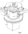
- FIG 1 shows a reactor 10 defining a chamber 11 in which are disposed an upper electrode 12 and a lower workpiece electrode 13.
- the upper electrode is connected to a R.F. supply whilst the lower electrode 13 is connected to a stress control unit generally indicated at 14.
- the workpiece 15 is seated on the lower electrode 13.
- the reactor 10 can be used for chemical deposition of a film onto the workpiece 15 in a manner which is generally well known.
- the method consists of striking a plasma within the chamber 11, which has previously been evacuated, and then introducing a working gas into the chamber; the gas being selected in accordance with the film which is required to be deposited.
- the plasma is set up by the R.F. present on the upper electrode.
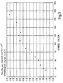
- Figure 3 shows a plot of stress against stress factor.
- the stress factor is actually represented in volts, but in essence an increasing stress factor value indicates an increasing effective resistance in a connection between the lower electrode 13 and ground.
- a low effective resistance produces a high compressive stress whilst high effective resistance produces tensile stress.
- the ideal working condition is the one at which compressive stress changes to tensile stress i.e. there is no effective stress in the film.
- this can be achieved by suitable selection of the stress factor.
- the value selected will differ from apparatus to apparatus and in accordance with the processing conditions, i.e. the nature of the working gas. However once determined for a particular set up, the stress factor can simply be selected or varied if difference stress characteristics are required.
- the stress control unit 14 comprises a connection 16 extending between the lower electrode 13 and ground.
- a transistor 17 is disposed in the connection 16 so as to control the rate of voltage drain from the electrode 13 to ground.
- the transistor 17 is controlled by a comparator 19, in the form of an operational amplifier, which compares the voltage at point 20 in the connection 16 with a set voltage set at 21 and drives the base of the transistor 17 so that the two voltages equate.
- the preset voltage can be varied to achieve selected stress values. It will be understood that the voltage at point 20 is directly proportional to the voltage on the workpiece 15 and so the result is a control of the workpiece voltage and hence the stress.
- circuits for controlling voltage protection could be used e.g. a variable resistance.
- the proposed circuit is particularly stable and easy to operate.
Landscapes
- Chemical & Material Sciences (AREA)
- Engineering & Computer Science (AREA)
- Physics & Mathematics (AREA)
- Plasma & Fusion (AREA)
- Analytical Chemistry (AREA)
- Chemical Kinetics & Catalysis (AREA)
- General Chemical & Material Sciences (AREA)
- Materials Engineering (AREA)
- Mechanical Engineering (AREA)
- Metallurgy (AREA)
- Organic Chemistry (AREA)
- Chemical Vapour Deposition (AREA)
- Application Of Or Painting With Fluid Materials (AREA)
- Luminescent Compositions (AREA)
- Physical Or Chemical Processes And Apparatus (AREA)
Abstract
Description
- This invention relates to apparatus and methods relating to the deposition of films on workpieces and in particular to the stress set up in those films during the deposition process.
- The need to deposit thin layers of material particularly arises in the manufacture of semi-conductor devices, but this invention is not limited to the manufacture of such devices. However, in that field it is generally recognised that it is desirable to attempt to control the stress set up in the film during deposition, because if not controlled the stresses can be sufficient to lift the film from the surface of the workpiece. It has been known for a long time that such stresses can be controlled, to a degree, by altering process parameters such as pressure, temperature, gas flow rates, etc. However, variations in these parameters generally cause variations in other physical characteristics of the film and so the user of this approach generally settles on a compromise.
- In plasma chemical vapour deposition processes it is known that the stress can be controlled by altering the frequency of the AC field which maintains the plasma discharge. However the frequency range in which stress is a minimum is also the band used for aircraft communication and so this technique is prohibited. Other proposals have been made for either switching between high and low frequency or providing a mix of frequencies but these too have their problems.
- JP-A-63317676, JP-A-62243765, and JP-A-58159843 all describe film forming or plating apparatus wherein a power supply is used to adjust the bias of a workpiece electrode support.
- According to the present invention there is provided Plasma Excited Chemical Vapour Deposition apparatus comprising a chamber radio frequency means for forming a plasma within the chamber, an electrode for supporting a workpiece, means for allowing gas to be introduced into the chamber such that a film can be deposited on the workpiece and means for connecting the electrode to ground by a variable resistance for draining the voltage from the electrode.
- From a further aspect the invention consists in Plasma Excited Chemical Vapour Deposition apparatus comprising a chamber, radio frequency means for forming a plasma within the chamber, an electrode for supporting a workpiece, means for allowing gas to be into the chamber such that a film can be deposited on the workpiece, means for connecting the electrode to ground and adjustable means for varying the effective resistance of the connection between the electrode and ground by adjusting the current flowing through the connecting means and/or the voltage dropped across the connecting means including a transistor connected to control the rate of voltage drain from the electrode to ground and means for comparing the voltage on the electrode, or an indication thereof, with a preset voltage and for controlling the transistor to equate the electrode and preset voltages or indications thereof.
- For the purposes of this specification the term "effective resistance" refers to the ease or otherwise with which a voltage on the electrode can drain to ground. It thus includes not only traditional resistance but also other means for affecting the current flow through the connection to ground.
- From a further aspect the invention consists in a method of controlling stress in Plasma Excited Chemical Vapour Deposition comprising placing a workpiece on an electrode in a reactor chamber, introducing a gas into the chamber, connecting the workpiece electrode to ground via a variable resistance and adjusting the resistance for draining the voltage on the electrode and thus maintaining a predetermined voltage on the electrode.
- The invention may be performed in various ways and a specific embodiment will now be described, by way of example, with reference to the accompanying drawings, in which:
- Figure 1 is a schematic cut away view of the apparatus according to the invention;
- Figure 2 is a schematic circuit diagram illustrating the power supply and stress control of the apparatus of Figure 1,
- Figure 3 is a graphical display of stress against "resistance" for a particular experimental set up using the apparatus of Figure 1, and
- Figure 4 is a diagrammatic representation showing the nature of a negative sheath formed above the workpiece electrode of the invention.
-
- Figure 1 shows a
reactor 10 defining achamber 11 in which are disposed anupper electrode 12 and alower workpiece electrode 13. As can be seen in Figure 2 the upper electrode is connected to a R.F. supply whilst thelower electrode 13 is connected to a stress control unit generally indicated at 14. Theworkpiece 15 is seated on thelower electrode 13. Thereactor 10 can be used for chemical deposition of a film onto theworkpiece 15 in a manner which is generally well known. In brief, the method consists of striking a plasma within thechamber 11, which has previously been evacuated, and then introducing a working gas into the chamber; the gas being selected in accordance with the film which is required to be deposited. The plasma is set up by the R.F. present on the upper electrode. - The existence of the plasma within the chamber causes a charge to be built up on the
lower electrode 13 due to capacitance. The Applicants have determined that, quite surprisingly, the stress formed in films deposited on the workpiece is a function of the level of charge existing on thelower electrode 13. A possible explanation for this is that due to the high mobility of electrons, everything in the chamber which is at a floating potential and in contact with the plasma takes on a negative charge. As this charge is accumulated, a "sheath" builds up which slows down the rate at which electrons can escape. The result is a quasi-neutrality in the plasma. If any part of the system is grounded the sheath is reduced to zero. It would appear that the stress in the workpiece is a function of the magnitude of the sheath. The formation of the sheath is diagrammatically illustrated in Figure 4. - Figure 3 shows a plot of stress against stress factor. For reasons, which will become apparent, the stress factor is actually represented in volts, but in essence an increasing stress factor value indicates an increasing effective resistance in a connection between the
lower electrode 13 and ground. As can be seen a low effective resistance produces a high compressive stress whilst high effective resistance produces tensile stress. It will be readily understood that the ideal working condition is the one at which compressive stress changes to tensile stress i.e. there is no effective stress in the film. As can be seen from the graph this can be achieved by suitable selection of the stress factor. The value selected will differ from apparatus to apparatus and in accordance with the processing conditions, i.e. the nature of the working gas. However once determined for a particular set up, the stress factor can simply be selected or varied if difference stress characteristics are required. - Returning to Figure 2, the
stress control unit 14 comprises aconnection 16 extending between thelower electrode 13 and ground. Atransistor 17 is disposed in theconnection 16 so as to control the rate of voltage drain from theelectrode 13 to ground. As the voltage on theworkpiece 15 is varying, it is convenient to also provide arectifier 18 in theconnection 16 between theelectrode 13 and ground. Thetransistor 17 is controlled by acomparator 19, in the form of an operational amplifier, which compares the voltage atpoint 20 in theconnection 16 with a set voltage set at 21 and drives the base of thetransistor 17 so that the two voltages equate. The preset voltage can be varied to achieve selected stress values. It will be understood that the voltage atpoint 20 is directly proportional to the voltage on theworkpiece 15 and so the result is a control of the workpiece voltage and hence the stress. - It will also be understood that other circuits for controlling voltage protection could be used e.g. a variable resistance. However the proposed circuit is particularly stable and easy to operate.
Claims (3)
- Plasma Excited Chemical Vapour Deposition apparatus comprising a chamber (11) radio frequency means for forming a plasma within the chamber, an electrode (13) for supporting a workpiece, means for allowing gas to be introduced into the chamber (11) such that a film can be deposited on the workpiece and means for connecting the electrode to ground by a variable resistance for draining the voltage from the electrode.
- Plasma Excited Chemical Vapour Deposition apparatus comprising a chamber(11), radio frequency means for forming a plasma within the chamber, an electrode (13) for supporting a workpiece, means (14) for allowing gas to be into the chamber such that a film can be deposited on the workpiece, means for connecting the electrode to ground and adjustable means for varying the effective resistance of the connection between the electrode and ground by adjusting the current flowing through the connecting means and/or the voltage dropped across the connecting means including a transistor (17) connected to control the rate of voltage drain from the electrode to ground and means (19) for comparing the voltage on the electrode, or an indication thereof, with a preset voltage and for controlling the transistor (17) to equate the electrode and preset voltages or indications thereof.
- A method of controlling stress in Plasma Excited Chemical Vapour Deposition comprising placing a workpiece on an electrode (13) in a reactor chamber (11), introducing a gas into the chamber (11), connecting the workpiece electrode (13) to ground via a variable resistance and adjusting the resistance for draining the voltage on the electrode and thus maintaining a predetermined voltage on the electrode.
Applications Claiming Priority (3)
| Application Number | Priority Date | Filing Date | Title |
|---|---|---|---|
| GB919125771A GB9125771D0 (en) | 1991-12-04 | 1991-12-04 | Deposition apparatus and methods |
| GB9125771 | 1991-12-04 | ||
| PCT/GB1992/002238 WO1993011276A1 (en) | 1991-12-04 | 1992-12-02 | Deposition apparatus and methods |
Publications (2)
| Publication Number | Publication Date |
|---|---|
| EP0650536A1 EP0650536A1 (en) | 1995-05-03 |
| EP0650536B1 true EP0650536B1 (en) | 2000-04-26 |
Family
ID=10705675
Family Applications (1)
| Application Number | Title | Priority Date | Filing Date |
|---|---|---|---|
| EP92924773A Expired - Lifetime EP0650536B1 (en) | 1991-12-04 | 1992-12-02 | Deposition apparatus and method |
Country Status (8)
| Country | Link |
|---|---|
| US (1) | US5492737A (en) |
| EP (1) | EP0650536B1 (en) |
| JP (1) | JP3392415B2 (en) |
| AT (1) | ATE192197T1 (en) |
| CA (1) | CA2124215A1 (en) |
| DE (1) | DE69230974T2 (en) |
| GB (1) | GB9125771D0 (en) |
| WO (1) | WO1993011276A1 (en) |
Families Citing this family (1)
| Publication number | Priority date | Publication date | Assignee | Title |
|---|---|---|---|---|
| DE4445177C5 (en) | 1994-11-22 | 2015-09-17 | Fraunhofer-Gesellschaft zur Förderung der angewandten Forschung e.V. | Method for producing micromechanical components with free-standing microstructures |
Family Cites Families (6)
| Publication number | Priority date | Publication date | Assignee | Title |
|---|---|---|---|---|
| DE3123427C2 (en) * | 1981-06-12 | 1985-10-24 | Siemens AG, 1000 Berlin und 8000 München | Arrangement for measuring the electrical resistance and the temperature of thin, metallically conductive layers deposited on substrates by vapor deposition or sputtering during the layer production |
| JPH062939B2 (en) * | 1982-03-16 | 1994-01-12 | 松下電器産業株式会社 | Thin film generation method |
| JPS60197875A (en) * | 1984-03-19 | 1985-10-07 | Ulvac Corp | Automatic film formation control device for sputtering device |
| JPS62243765A (en) * | 1986-04-15 | 1987-10-24 | Sumitomo Heavy Ind Ltd | Method for relieving residual stress in stage of forming thin film |
| JPS63317676A (en) * | 1987-06-19 | 1988-12-26 | Sharp Corp | Production of thin metallic compound film having non-grained structure |
| CA2014540A1 (en) * | 1989-04-18 | 1990-10-18 | Mitsui Toatsu Chemicals, Inc. | Method for forming semiconductor thin film |
-
1991
- 1991-12-04 GB GB919125771A patent/GB9125771D0/en active Pending
-
1992
- 1992-12-02 US US08/244,573 patent/US5492737A/en not_active Expired - Fee Related
- 1992-12-02 WO PCT/GB1992/002238 patent/WO1993011276A1/en not_active Ceased
- 1992-12-02 JP JP50996593A patent/JP3392415B2/en not_active Expired - Fee Related
- 1992-12-02 AT AT92924773T patent/ATE192197T1/en active
- 1992-12-02 CA CA002124215A patent/CA2124215A1/en not_active Abandoned
- 1992-12-02 EP EP92924773A patent/EP0650536B1/en not_active Expired - Lifetime
- 1992-12-02 DE DE69230974T patent/DE69230974T2/en not_active Expired - Fee Related
Also Published As
| Publication number | Publication date |
|---|---|
| US5492737A (en) | 1996-02-20 |
| JPH07501583A (en) | 1995-02-16 |
| WO1993011276A1 (en) | 1993-06-10 |
| ATE192197T1 (en) | 2000-05-15 |
| GB9125771D0 (en) | 1992-02-05 |
| JP3392415B2 (en) | 2003-03-31 |
| DE69230974T2 (en) | 2000-10-19 |
| CA2124215A1 (en) | 1993-06-10 |
| DE69230974D1 (en) | 2000-05-31 |
| EP0650536A1 (en) | 1995-05-03 |
Similar Documents
| Publication | Publication Date | Title |
|---|---|---|
| DE60130092T2 (en) | Method for heating platelets | |
| US10109462B2 (en) | Dual radio-frequency tuner for process control of a plasma process | |
| US10685862B2 (en) | Controlling the RF amplitude of an edge ring of a capacitively coupled plasma process device | |
| US5556520A (en) | Method for controlling a reactive sputtering process | |
| US9190302B2 (en) | System and method for controlling plasma with an adjustable coupling to ground circuit | |
| KR102649738B1 (en) | Film stress control for plasma-enhanced chemical vapor deposition | |
| US6239403B1 (en) | Power segmented electrode | |
| US5180476A (en) | Method for producing transparent conductive films | |
| US5630949A (en) | Method and apparatus for fabricating a piezoelectric resonator to a resonant frequency | |
| KR100276093B1 (en) | Plasma etching system | |
| US5532190A (en) | Plasma treatment method in electronic device manufacture | |
| EP0003020B1 (en) | High frequency sputtering apparatus | |
| KR101545525B1 (en) | Apparatus and method for processing a substrate edge region | |
| US3617459A (en) | Rf sputtering method and apparatus for producing insulating films of varied physical properties | |
| CA1211867A (en) | Method and apparatus for fabricating devices with dc bias-controlled reactive ion etching | |
| US20060191637A1 (en) | Etching Apparatus and Process with Thickness and Uniformity Control | |
| CN109961997B (en) | Plasma processing apparatus and DC bias voltage control method thereof | |
| EP0390127A3 (en) | Method for vaporizing and supplying organometal compounds and apparatus for carrying out the method | |
| JP2003234200A (en) | Plasma impedance adjustment device | |
| US5492737A (en) | Deposition apparatus and method | |
| DE69927146T2 (en) | METHOD AND DEVICE FOR CHANGING THE PROFILE OF GAPS WITH HIGH ASPECT RATIO THROUGH THE USE OF DIFFERENTIAL PLASMA ENERGY | |
| EP0266604A2 (en) | Anode plate for a parallel-plate reactive ion etching reactor | |
| JP7624120B2 (en) | DC plasma control for electron-assisted materials processing. | |
| US5861103A (en) | Etching method and apparatus | |
| US4533450A (en) | Control of the hydrogen bonding in reactively sputtered amorphous silicon |
Legal Events
| Date | Code | Title | Description |
|---|---|---|---|
| PUAI | Public reference made under article 153(3) epc to a published international application that has entered the european phase |
Free format text: ORIGINAL CODE: 0009012 |
|
| 17P | Request for examination filed |
Effective date: 19940607 |
|
| AK | Designated contracting states |
Kind code of ref document: A1 Designated state(s): AT CH DE ES FR GB IE IT LI NL |
|
| 17Q | First examination report despatched |
Effective date: 19960115 |
|
| GRAG | Despatch of communication of intention to grant |
Free format text: ORIGINAL CODE: EPIDOS AGRA |
|
| GRAG | Despatch of communication of intention to grant |
Free format text: ORIGINAL CODE: EPIDOS AGRA |
|
| GRAH | Despatch of communication of intention to grant a patent |
Free format text: ORIGINAL CODE: EPIDOS IGRA |
|
| RAP1 | Party data changed (applicant data changed or rights of an application transferred) |
Owner name: TRIKON EQUIPMENTS LIMITED |
|
| GRAH | Despatch of communication of intention to grant a patent |
Free format text: ORIGINAL CODE: EPIDOS IGRA |
|
| GRAA | (expected) grant |
Free format text: ORIGINAL CODE: 0009210 |
|
| AK | Designated contracting states |
Kind code of ref document: B1 Designated state(s): AT CH DE ES FR GB IE IT LI NL |
|
| PG25 | Lapsed in a contracting state [announced via postgrant information from national office to epo] |
Ref country code: ES Free format text: THE PATENT HAS BEEN ANNULLED BY A DECISION OF A NATIONAL AUTHORITY Effective date: 20000426 Ref country code: AT Free format text: LAPSE BECAUSE OF FAILURE TO SUBMIT A TRANSLATION OF THE DESCRIPTION OR TO PAY THE FEE WITHIN THE PRESCRIBED TIME-LIMIT Effective date: 20000426 |
|
| REF | Corresponds to: |
Ref document number: 192197 Country of ref document: AT Date of ref document: 20000515 Kind code of ref document: T |
|
| REG | Reference to a national code |
Ref country code: CH Ref legal event code: EP |
|
| ITF | It: translation for a ep patent filed | ||
| REF | Corresponds to: |
Ref document number: 69230974 Country of ref document: DE Date of ref document: 20000531 |
|
| REG | Reference to a national code |
Ref country code: CH Ref legal event code: NV Representative=s name: MOINAS SAVOYE & CRONIN Ref country code: IE Ref legal event code: FG4D |
|
| ET | Fr: translation filed | ||
| PLBE | No opposition filed within time limit |
Free format text: ORIGINAL CODE: 0009261 |
|
| STAA | Information on the status of an ep patent application or granted ep patent |
Free format text: STATUS: NO OPPOSITION FILED WITHIN TIME LIMIT |
|
| 26N | No opposition filed | ||
| PGFP | Annual fee paid to national office [announced via postgrant information from national office to epo] |
Ref country code: IE Payment date: 20011205 Year of fee payment: 10 |
|
| PGFP | Annual fee paid to national office [announced via postgrant information from national office to epo] |
Ref country code: CH Payment date: 20011227 Year of fee payment: 10 |
|
| PGFP | Annual fee paid to national office [announced via postgrant information from national office to epo] |
Ref country code: NL Payment date: 20011228 Year of fee payment: 10 |
|
| REG | Reference to a national code |
Ref country code: GB Ref legal event code: IF02 |
|
| PG25 | Lapsed in a contracting state [announced via postgrant information from national office to epo] |
Ref country code: IE Free format text: LAPSE BECAUSE OF NON-PAYMENT OF DUE FEES Effective date: 20021202 |
|
| PGFP | Annual fee paid to national office [announced via postgrant information from national office to epo] |
Ref country code: FR Payment date: 20021212 Year of fee payment: 11 |
|
| PG25 | Lapsed in a contracting state [announced via postgrant information from national office to epo] |
Ref country code: LI Free format text: LAPSE BECAUSE OF NON-PAYMENT OF DUE FEES Effective date: 20021231 Ref country code: CH Free format text: LAPSE BECAUSE OF NON-PAYMENT OF DUE FEES Effective date: 20021231 |
|
| PGFP | Annual fee paid to national office [announced via postgrant information from national office to epo] |
Ref country code: DE Payment date: 20030228 Year of fee payment: 11 |
|
| PG25 | Lapsed in a contracting state [announced via postgrant information from national office to epo] |
Ref country code: NL Free format text: LAPSE BECAUSE OF NON-PAYMENT OF DUE FEES Effective date: 20030701 |
|
| REG | Reference to a national code |
Ref country code: CH Ref legal event code: PL |
|
| NLV4 | Nl: lapsed or anulled due to non-payment of the annual fee |
Effective date: 20030701 |
|
| REG | Reference to a national code |
Ref country code: IE Ref legal event code: MM4A |
|
| PG25 | Lapsed in a contracting state [announced via postgrant information from national office to epo] |
Ref country code: DE Free format text: LAPSE BECAUSE OF NON-PAYMENT OF DUE FEES Effective date: 20040701 |
|
| PG25 | Lapsed in a contracting state [announced via postgrant information from national office to epo] |
Ref country code: FR Free format text: LAPSE BECAUSE OF NON-PAYMENT OF DUE FEES Effective date: 20040831 |
|
| REG | Reference to a national code |
Ref country code: FR Ref legal event code: ST |
|
| PG25 | Lapsed in a contracting state [announced via postgrant information from national office to epo] |
Ref country code: IT Free format text: LAPSE BECAUSE OF NON-PAYMENT OF DUE FEES;WARNING: LAPSES OF ITALIAN PATENTS WITH EFFECTIVE DATE BEFORE 2007 MAY HAVE OCCURRED AT ANY TIME BEFORE 2007. THE CORRECT EFFECTIVE DATE MAY BE DIFFERENT FROM THE ONE RECORDED. Effective date: 20051202 |
|
| PGFP | Annual fee paid to national office [announced via postgrant information from national office to epo] |
Ref country code: GB Payment date: 20061222 Year of fee payment: 15 |
|
| GBPC | Gb: european patent ceased through non-payment of renewal fee |
Effective date: 20071202 |
|
| PG25 | Lapsed in a contracting state [announced via postgrant information from national office to epo] |
Ref country code: GB Free format text: LAPSE BECAUSE OF NON-PAYMENT OF DUE FEES Effective date: 20071202 |