EP0644409B1 - A method of remotely measuring process data - Google Patents
A method of remotely measuring process data Download PDFInfo
- Publication number
- EP0644409B1 EP0644409B1 EP94306773A EP94306773A EP0644409B1 EP 0644409 B1 EP0644409 B1 EP 0644409B1 EP 94306773 A EP94306773 A EP 94306773A EP 94306773 A EP94306773 A EP 94306773A EP 0644409 B1 EP0644409 B1 EP 0644409B1
- Authority
- EP
- European Patent Office
- Prior art keywords
- silicon
- wafer
- monitor element
- primary coil
- temperature
- Prior art date
- Legal status (The legal status is an assumption and is not a legal conclusion. Google has not performed a legal analysis and makes no representation as to the accuracy of the status listed.)
- Expired - Lifetime
Links
Images

Classifications
-
- H—ELECTRICITY
- H10—SEMICONDUCTOR DEVICES; ELECTRIC SOLID-STATE DEVICES NOT OTHERWISE PROVIDED FOR
- H10P—GENERIC PROCESSES OR APPARATUS FOR THE MANUFACTURE OR TREATMENT OF DEVICES COVERED BY CLASS H10
- H10P72/00—Handling or holding of wafers, substrates or devices during manufacture or treatment thereof
- H10P72/06—Apparatus for monitoring, sorting, marking, testing or measuring
- H10P72/0602—Temperature monitoring
-
- G—PHYSICS
- G01—MEASURING; TESTING
- G01K—MEASURING TEMPERATURE; MEASURING QUANTITY OF HEAT; THERMALLY-SENSITIVE ELEMENTS NOT OTHERWISE PROVIDED FOR
- G01K1/00—Details of thermometers not specially adapted for particular types of thermometer
- G01K1/02—Means for indicating or recording specially adapted for thermometers
- G01K1/024—Means for indicating or recording specially adapted for thermometers for remote indication
-
- G—PHYSICS
- G01—MEASURING; TESTING
- G01K—MEASURING TEMPERATURE; MEASURING QUANTITY OF HEAT; THERMALLY-SENSITIVE ELEMENTS NOT OTHERWISE PROVIDED FOR
- G01K7/00—Measuring temperature based on the use of electric or magnetic elements directly sensitive to heat ; Power supply therefor, e.g. using thermoelectric elements
-
- H—ELECTRICITY
- H10—SEMICONDUCTOR DEVICES; ELECTRIC SOLID-STATE DEVICES NOT OTHERWISE PROVIDED FOR
- H10P—GENERIC PROCESSES OR APPARATUS FOR THE MANUFACTURE OR TREATMENT OF DEVICES COVERED BY CLASS H10
- H10P72/00—Handling or holding of wafers, substrates or devices during manufacture or treatment thereof
- H10P72/04—Apparatus for manufacture or treatment
- H10P72/0431—Apparatus for thermal treatment
- H10P72/0432—Apparatus for thermal treatment mainly by conduction
Definitions
- the present invention relates to a method of remotely sensing temperature conditions at the location of silicon wafers undergoing a process.
- EP-A-0406751 discloses an apparatus for sensing process conditions during a process in which a plurality of elements are fabricated and employing a monitor element for assisting in sensing the process conditions and WO-A-8601595 discloses a thermometer arrangement including an inductor structure serving to provide for a contactless temperature measuring arrangement.
- the impedance of the silicon wafer monitor element can be determined by changes in current amplitude and phase within the primary coil.
- the monitor wafer 10 (Fig. 2), which does not form an embodiment of the invention, is prepared for use by forming a structure 12 on its surface, which structure subsequently acts as the secondary current loop of a transformer.
- This structure may be considered to be a circular transmission line whose characteristic capacitance and resistive impedances vary in a predetermined fashion with ambient conditions such as temperature. For a given structure and set of ambient conditions, this secondary current loop may be expected to have a characteristic resonant frequency.
- a representation 14 of the secondary current loop is shown as comprised of a circuit 16 including a plurality of capacitances 18 and a plurality of resistances 20.
- the circuit 16 is shown as located in operative relationship with a representation of a transformer structure 22 which includes a primary coil 24, a current source 26 and a sensing device 28 which is capable of sensing electrical measurements from the primary coil 24.
- the secondary current loop need not be a closed continuous current loop structure shown in Fig. 2.
- Other appropriate configuration can be employed, if desired.
- One such configuration which does also not form an embodiment of the invention, is shown in Fig. 4, in which a portion of a spiral 44 is located on a surface 46 of a wafer 48. The ends of the spiral segment are joined by a conductive, resistive or semiconductive strap 50 which is insulated by a suitable insulating layer (not shown) from the portions of the spiral 44 over which it passes.
- a silicon wafer without a loop structure thereon employed as a monitor wafer is a silicon wafer without a loop structure thereon employed as a monitor wafer. Locating such a wafer in operative relation with respect to the primary coil of a transformer structure and the application of power to the primary coil will induce eddy currents in the wafer, which in turn will affect the electrical measurements taken from the transformer structure by a sensing device. These measurements may then be used, after proper calibration, to determine desired data, such as temperature, relating to the monitor wafer. Since the monitor wafer is made of the same material and has the same configuration as the wafers actually being processed, this same temperature or other value is also applicable to the wafers being processed.
- the present invention may find use in a number of different applications.
- One such application is in the periodic determination of temperature of a group or batch of silicon wafers which are being processed in the course of manufacture of semiconductor devices. In such a process, it is desirable to avoid actual contact with the silicon wafers in order to avoid possible contamination.
- a monitor wafer being made from the same material and having the same configuration as the wafers being processed, can be included in the batch of wafers being processed, and its temperature, which will be essentially identical to the temperature of the other wafers in the batch, can be ascertained.
Landscapes
- Physics & Mathematics (AREA)
- General Physics & Mathematics (AREA)
- Testing Or Measuring Of Semiconductors Or The Like (AREA)
- Measuring Instrument Details And Bridges, And Automatic Balancing Devices (AREA)
Description
- The present invention relates to a method of remotely sensing temperature conditions at the location of silicon wafers undergoing a process.
- One measurement method in current use involves an optical measurement which measures the black body radiation spectrum or a portion of it which is a function of temperature. This measurement is highly dependent upon the surface conditions of the substrate being measured and is therefore difficult to make.
- Another measurement method involves the use of a thermocouple. This method is also difficult to carry out because it requires good contact with the wafer for fast and accurate measurements.
- EP-A-0406751 discloses an apparatus for sensing process conditions during a process in which a plurality of elements are fabricated and employing a monitor element for assisting in sensing the process conditions and WO-A-8601595 discloses a thermometer arrangement including an inductor structure serving to provide for a contactless temperature measuring arrangement.
- It is an object of the present invention to provide a method of measuring temperature conditions of silicon wafers being processed, which overcomes the aforementioned difficulties.
- According to the present invention there is provided a method of monitoring temperature conditions of a plurality of silicon wafers during a silicon wafer fabrication process, characterized by the steps of introducing a silicon-wafer-monitor element similar in material and shape to the said silicon wafers into the process in addition to the said silicon wafers and having electrical characteristics determined by its temperature, inductively coupling the said silicon-wafer-monitor element to a primary coil forming part of a primary inductor structure while the said silicon wafers and the said silicon-wafer-monitor element are exposed to the said processing conditions, the primary inductor structure further comprising a current source and a sensor connected to the said primary coil so as to inductively couple eddy currents in the silicon-wafer-monitor element, sensing changes in an electrical signal in the primary coil with the sensor, the changes in the signal being induced by variations of the eddy currents in the silicon-wafer-monitor element, and converting the sensed changes to a temperature value.
- It will be appreciated that the impedance of the silicon wafer monitor element can be determined by changes in current amplitude and phase within the primary coil.
- The examples shown in Fig. 1-4 are not covered by the claims but provide examples which are useful for understanding the invention.
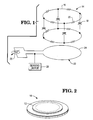
- Fig. 1 shows a schematic approximation of a secondary current loop comprising an RC circuit on a wafer which is inductively coupled to a primary coil of a transformer and sensing structure;
- Fig. 2 is a diagrammatic view of a closed secondary current loop which has been deposited on a substrate;
- Fig. 3 is a diagrammatic view of a wafer located in operative relation to a transformer and sensing structure; and
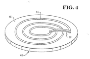
- Fig. 4 is a diagrammatic view of a spiral segment with connecting strap which has been deposited on a substrate;
-
- The monitor wafer 10 (Fig. 2), which does not form an embodiment of the invention, is prepared for use by forming a
structure 12 on its surface, which structure subsequently acts as the secondary current loop of a transformer. This structure may be considered to be a circular transmission line whose characteristic capacitance and resistive impedances vary in a predetermined fashion with ambient conditions such as temperature. For a given structure and set of ambient conditions, this secondary current loop may be expected to have a characteristic resonant frequency. In Fig. 1, arepresentation 14 of the secondary current loop is shown as comprised of acircuit 16 including a plurality ofcapacitances 18 and a plurality ofresistances 20. Thecircuit 16 is shown as located in operative relationship with a representation of atransformer structure 22 which includes aprimary coil 24, acurrent source 26 and asensing device 28 which is capable of sensing electrical measurements from theprimary coil 24. - A similar arrangement, which does also not form an embodiment of the invention, is shown in Fig. 3, in which a
transformer structure 30 includes two coupledprimary coils current source 36 and asensing device 38. Asecondary coil 40 forms part of amonitor wafer 42 which is positioned between theprimary coils - The secondary current loop need not be a closed continuous current loop structure shown in Fig. 2. Other appropriate configuration can be employed, if desired. One such configuration, which does also not form an embodiment of the invention, is shown in Fig. 4, in which a portion of a
spiral 44 is located on asurface 46 of awafer 48. The ends of the spiral segment are joined by a conductive, resistive orsemiconductive strap 50 which is insulated by a suitable insulating layer (not shown) from the portions of thespiral 44 over which it passes. - In an embodiment of the invention is a silicon wafer without a loop structure thereon employed as a monitor wafer. Locating such a wafer in operative relation with respect to the primary coil of a transformer structure and the application of power to the primary coil will induce eddy currents in the wafer, which in turn will affect the electrical measurements taken from the transformer structure by a sensing device. These measurements may then be used, after proper calibration, to determine desired data, such as temperature, relating to the monitor wafer. Since the monitor wafer is made of the same material and has the same configuration as the wafers actually being processed, this same temperature or other value is also applicable to the wafers being processed.
- The present invention may find use in a number of different applications. One such application is in the periodic determination of temperature of a group or batch of silicon wafers which are being processed in the course of manufacture of semiconductor devices. In such a process, it is desirable to avoid actual contact with the silicon wafers in order to avoid possible contamination. Accordingly, a monitor wafer, being made from the same material and having the same configuration as the wafers being processed, can be included in the batch of wafers being processed, and its temperature, which will be essentially identical to the temperature of the other wafers in the batch, can be ascertained. This can be done without actual physical contact with the monitor wafer, as shown in Fig.3, by causing a monitor wafer to come into operative relation with the
primary coils transformer structure 30, and detecting by use of thesensing device 38 the resulting change in electrical characteristics. By appropriate calibration, the change in electrical characteristics can be converted to indicate the temperature of the monitor wafer, which will be essentially identical to the temperature of the actual wafers being processed and a change in internal eddy currents, when exposed to the field from the primary coils of the transformer structure, is relied upon to produce a change in the current in the primary coils which can be sensed by a sensing device and converted to a temperature value.
Claims (2)
- A method of monitoring temperature conditions of a plurality of silicon wafers during a silicon wafer fabrication process, characterized by the steps of introducing a silicon-wafer-monitor element similar in material and shape to the said silicon wafers into the process in addition to the said silicon wafers and having electrical characteristics determined by its temperature, inductively coupling the said silicon-wafer-monitor element to a primary coil (32, 34) forming part of a primary inductor structure (30) while the said silicon wafers and the said silicon-wafer-monitor element are exposed to the said processing conditions, the primary inductor structure further comprising a current source (36) and a sensor (38) connected to the said primary coil (32, 34) so as to inductively couple eddy currents in the silicon-wafer-monitor element, sensing changes in an electrical signal in the primary coil (32, 34) with the sensor (38), the changes in the signal being induced by variations of the eddy currents in the silicon-wafer-monitor element, and converting the sensed changes to a temperature value.
- A method according to Claim 1, characterized in that the said electrical signal comprises current amplitude and the impedance of the silicon-wafer-monitor element is determined by changes in the current amplitude and phase within said primary coil (32, 34).
Applications Claiming Priority (2)
| Application Number | Priority Date | Filing Date | Title |
|---|---|---|---|
| US123664 | 1993-09-20 | ||
| US08/123,664 US5466614A (en) | 1993-09-20 | 1993-09-20 | Structure and method for remotely measuring process data |
Publications (3)
| Publication Number | Publication Date |
|---|---|
| EP0644409A2 EP0644409A2 (en) | 1995-03-22 |
| EP0644409A3 EP0644409A3 (en) | 1995-04-19 |
| EP0644409B1 true EP0644409B1 (en) | 2001-08-29 |
Family
ID=22410077
Family Applications (1)
| Application Number | Title | Priority Date | Filing Date |
|---|---|---|---|
| EP94306773A Expired - Lifetime EP0644409B1 (en) | 1993-09-20 | 1994-09-15 | A method of remotely measuring process data |
Country Status (4)
| Country | Link |
|---|---|
| US (2) | US5466614A (en) |
| EP (1) | EP0644409B1 (en) |
| JP (1) | JP3787644B2 (en) |
| DE (1) | DE69428086T2 (en) |
Families Citing this family (19)
| Publication number | Priority date | Publication date | Assignee | Title |
|---|---|---|---|---|
| US5902044A (en) * | 1997-06-27 | 1999-05-11 | International Business Machines Corporation | Integrated hot spot detector for design, analysis, and control |
| US6030877A (en) * | 1997-10-06 | 2000-02-29 | Industrial Technology Research Institute | Electroless gold plating method for forming inductor structures |
| US6278379B1 (en) * | 1998-04-02 | 2001-08-21 | Georgia Tech Research Corporation | System, method, and sensors for sensing physical properties |
| DE19910983A1 (en) * | 1999-03-12 | 2000-09-21 | Bosch Gmbh Robert | Device and method for determining the lateral undercut of a structured surface layer |
| KR100674624B1 (en) * | 1999-05-07 | 2007-01-25 | 동경 엘렉트론 주식회사 | Sensor substrate, substrate processing method and substrate processing apparatus |
| JP2001242014A (en) * | 2000-02-29 | 2001-09-07 | Tokyo Electron Ltd | Substrate temperature measuring method and processing method |
| US20020045237A1 (en) * | 2000-03-29 | 2002-04-18 | Gouzel Karimova | Bacterial two-hybrid system for protein-protein interaction screening, new strains for use therein, and their applications |
| CA2414724C (en) * | 2002-12-18 | 2011-02-22 | Cashcode Company Inc. | Induction sensor using printed circuit |
| TWI268429B (en) * | 2003-11-29 | 2006-12-11 | Onwafer Technologies Inc | Systems, maintenance units and substrate processing systems for wirelessly charging and wirelessly communicating with sensor apparatus as well as methods for wirelessly charging and communicating with sensor apparatus |
| KR100601956B1 (en) * | 2004-06-28 | 2006-07-14 | 삼성전자주식회사 | Temperature measuring device using change of magnetic field |
| JP4859610B2 (en) | 2006-09-29 | 2012-01-25 | 富士通セミコンダクター株式会社 | Buffer circuit and control method thereof |
| JP5049018B2 (en) * | 2007-01-09 | 2012-10-17 | ソニーモバイルコミュニケーションズ株式会社 | Non-contact charger |
| JP5478874B2 (en) * | 2008-12-02 | 2014-04-23 | 株式会社フィルテック | Substrate, substrate holding device, analysis device, program, detection system, semiconductor device, display device, and semiconductor manufacturing device |
| US8226294B2 (en) * | 2009-08-31 | 2012-07-24 | Arizant Healthcare Inc. | Flexible deep tissue temperature measurement devices |
| US8292495B2 (en) * | 2010-04-07 | 2012-10-23 | Arizant Healthcare Inc. | Zero-heat-flux, deep tissue temperature measurement devices with thermal sensor calibration |
| US8292502B2 (en) * | 2010-04-07 | 2012-10-23 | Arizant Healthcare Inc. | Constructions for zero-heat-flux, deep tissue temperature measurement devices |
| US9354122B2 (en) | 2011-05-10 | 2016-05-31 | 3M Innovative Properties Company | Zero-heat-flux, deep tissue temperature measurement system |
| JP2016524130A (en) * | 2013-05-03 | 2016-08-12 | スリーエム イノベイティブ プロパティズ カンパニー | Electrical conductor temperature monitoring system |
| AU2022388907A1 (en) * | 2021-11-17 | 2024-06-27 | Caretech Services Pty Ltd | A temperature detector for a heat sensitive material |
Family Cites Families (27)
| Publication number | Priority date | Publication date | Assignee | Title |
|---|---|---|---|---|
| US2989691A (en) * | 1956-05-28 | 1961-06-20 | Gen Electric | Temperature measuring apparatus |
| US3350760A (en) * | 1959-02-06 | 1967-11-07 | Texas Instruments Inc | Capacitor for miniature electronic circuits or the like |
| US3234461A (en) * | 1960-12-05 | 1966-02-08 | Texas Instruments Inc | Resistivity-measuring device including solid inductive sensor |
| US3338100A (en) * | 1963-06-12 | 1967-08-29 | Hitachi Ltd | Non-contact resonant thermometer |
| US3320495A (en) * | 1963-07-02 | 1967-05-16 | Atomic Energy Commission | Surface-barrier diode for detecting high energy particles and method for preparing same |
| US3391576A (en) * | 1965-03-13 | 1968-07-09 | Hitachi Ltd | Thermometric device for rotating structures |
| US3544893A (en) * | 1968-08-05 | 1970-12-01 | Anatoly Ivanovich Savin | Apparatus for noncontact measurement of semiconductor resistivity including a toroidal inductive coil with a gap |
| US3781506A (en) * | 1972-07-28 | 1973-12-25 | Gen Electric | Non-contacting temperature measurement of inductively heated utensil and other objects |
| US4000458A (en) * | 1975-08-21 | 1976-12-28 | Bell Telephone Laboratories, Incorporated | Method for the noncontacting measurement of the electrical conductivity of a lamella |
| JPS52111775A (en) * | 1976-03-17 | 1977-09-19 | Nippon Kokan Kk | Temperature measuring instrument and method of using same |
| US4333225A (en) * | 1978-12-18 | 1982-06-08 | Xerox Corporation | Method of making a circular high voltage field effect transistor |
| JPS5648145A (en) * | 1979-09-28 | 1981-05-01 | Hitachi Ltd | Measurement for sheet resistance of semiconductor layer |
| DE3113557C2 (en) * | 1981-04-03 | 1984-04-26 | Siemens AG, 1000 Berlin und 8000 München | Electrical measuring device for the rotor temperature of electrical machines |
| US4457794A (en) * | 1982-06-25 | 1984-07-03 | Matsushita Electric Industrial Co., Ltd. | Method for manufacturing optical memory disc |
| GB8422360D0 (en) * | 1984-09-05 | 1984-10-10 | Kon I | Thermometers |
| EP0261353A3 (en) * | 1986-09-24 | 1989-02-01 | Grapha-Holding Ag | Measuring unit |
| JPH065691B2 (en) * | 1987-09-26 | 1994-01-19 | 株式会社東芝 | Semiconductor element test method and test apparatus |
| JPH0623935B2 (en) * | 1988-02-09 | 1994-03-30 | 大日本スクリーン製造株式会社 | Heat treatment control method with improved reproducibility |
| EP0359922A1 (en) * | 1988-09-13 | 1990-03-28 | Landis & Gyr Betriebs AG | Apparatus for magnetic-field measurement |
| NL8901079A (en) * | 1989-04-28 | 1990-11-16 | Nedap Nv | PASSIVE ELECTRONIC RECORDER. |
| EP0406751A1 (en) * | 1989-07-07 | 1991-01-09 | Balzers Aktiengesellschaft | Method and apparatus for the acquisition of measured data during the treatment of disks |
| CA2045507A1 (en) * | 1989-11-09 | 1991-05-10 | Arthur F. Hogrefe | Inductive coupled high temperature monitor |
| JPH07113664B2 (en) * | 1990-02-26 | 1995-12-06 | シャープ株式会社 | Superconducting magnetic field distribution measuring device |
| US5119025A (en) * | 1990-07-26 | 1992-06-02 | Eastman Kodak Company | High-sensitivity magnetorresistive magnetometer having laminated flux collectors defining an open-loop flux-conducting path |
| US5288649A (en) * | 1991-09-30 | 1994-02-22 | Texas Instruments Incorporated | Method for forming uncooled infrared detector |
| US5370766A (en) * | 1993-08-16 | 1994-12-06 | California Micro Devices | Methods for fabrication of thin film inductors, inductor networks and integration with other passive and active devices |
| US5439850A (en) * | 1993-09-08 | 1995-08-08 | North Carolina State University | Method for forming a layer of uniform thickness on a semiconductor wafer during rapid thermal processing |
-
1993
- 1993-09-20 US US08/123,664 patent/US5466614A/en not_active Expired - Lifetime
-
1994
- 1994-08-25 JP JP20001094A patent/JP3787644B2/en not_active Expired - Lifetime
- 1994-09-15 DE DE69428086T patent/DE69428086T2/en not_active Expired - Fee Related
- 1994-09-15 EP EP94306773A patent/EP0644409B1/en not_active Expired - Lifetime
-
1995
- 1995-06-02 US US08/460,287 patent/US5576224A/en not_active Expired - Lifetime
Also Published As
| Publication number | Publication date |
|---|---|
| US5466614A (en) | 1995-11-14 |
| JPH07106392A (en) | 1995-04-21 |
| US5576224A (en) | 1996-11-19 |
| DE69428086T2 (en) | 2002-03-28 |
| EP0644409A2 (en) | 1995-03-22 |
| DE69428086D1 (en) | 2001-10-04 |
| JP3787644B2 (en) | 2006-06-21 |
| EP0644409A3 (en) | 1995-04-19 |
Similar Documents
| Publication | Publication Date | Title |
|---|---|---|
| US5466614A (en) | Structure and method for remotely measuring process data | |
| US5472561A (en) | Radio frequency monitor for semiconductor process control | |
| US7960670B2 (en) | Methods of and apparatuses for measuring electrical parameters of a plasma process | |
| US4797614A (en) | Apparatus and method for measuring conductance including a temperature controlled resonant tank circuit with shielding | |
| US20060114004A1 (en) | Method for calibrating and de-embedding, set of devices for de-embedding and vector network analyzer | |
| US3234461A (en) | Resistivity-measuring device including solid inductive sensor | |
| US4649495A (en) | Process and device for measuring the initial permeability of ferrimagnetic materials over a wide frequency band | |
| KR100389277B1 (en) | Sheet resistance meter | |
| US6448795B1 (en) | Three coil apparatus for inductive measurements of conductance | |
| JP2001242014A (en) | Substrate temperature measuring method and processing method | |
| KR101252885B1 (en) | Methods and apparatus for optimizing an electrical response to a conductive layer on a substrate | |
| EP0515356B1 (en) | Method and apparatus for measuring the temperature of an electrically conductive material | |
| US5485080A (en) | Non-contact measurement of linewidths of conductors in semiconductor device structures | |
| US4874252A (en) | Electronic thermometer | |
| JPH0664011B2 (en) | Method and device for detecting electric conductivity of sample made of superconducting material | |
| EP0104748A1 (en) | RF Watt meter | |
| KR20080022556A (en) | Method and apparatus for optimizing electrical response for a set of conductive layers on a substrate | |
| Dharmasena et al. | Eddy current sensor concepts for the Bridgman growth of semiconductors | |
| US3430132A (en) | Magnetic thickness measuring apparatus utilizing one fixed and one movable measuring coil | |
| SU1763960A1 (en) | Relative humidity and temperature detector | |
| Katzmann et al. | A new optically sensed thermal element for precise ac-dc conversion | |
| JPH06331454A (en) | Temperature measuring device | |
| Morrison et al. | A method of determining and monitoring power and impedance at high frequencies | |
| Huang et al. | Experimental studies of the RF-DC differences of voltage standards | |
| JPS5821395B2 (en) | How do you know what to do? |
Legal Events
| Date | Code | Title | Description |
|---|---|---|---|
| PUAI | Public reference made under article 153(3) epc to a published international application that has entered the european phase |
Free format text: ORIGINAL CODE: 0009012 |
|
| PUAL | Search report despatched |
Free format text: ORIGINAL CODE: 0009013 |
|
| AK | Designated contracting states |
Kind code of ref document: A2 Designated state(s): DE FR GB |
|
| AK | Designated contracting states |
Kind code of ref document: A3 Designated state(s): DE FR GB |
|
| RAP1 | Party data changed (applicant data changed or rights of an application transferred) |
Owner name: HYUNDAI ELECTRONICS AMERICA Owner name: AT&T GLOBAL INFORMATION SOLUTIONS INTERNATIONAL IN |
|
| 17P | Request for examination filed |
Effective date: 19950909 |
|
| RAP1 | Party data changed (applicant data changed or rights of an application transferred) |
Owner name: SYMBIOS LOGIC INC. Owner name: HYUNDAI ELECTRONICS AMERICA Owner name: AT&T GLOBAL INFORMATION SOLUTIONS INTERNATIONAL IN |
|
| RAP1 | Party data changed (applicant data changed or rights of an application transferred) |
Owner name: SYMBIOS LOGIC INC. Owner name: HYUNDAI ELECTRONICS AMERICA Owner name: NCR INTERNATIONAL, INC. |
|
| 17Q | First examination report despatched |
Effective date: 19980115 |
|
| RAP1 | Party data changed (applicant data changed or rights of an application transferred) |
Owner name: SYMBIOS, INC. Owner name: HYUNDAI ELECTRONICS AMERICA Owner name: NCR INTERNATIONAL, INC. |
|
| GRAG | Despatch of communication of intention to grant |
Free format text: ORIGINAL CODE: EPIDOS AGRA |
|
| RTI1 | Title (correction) |
Free format text: A METHOD OF REMOTELY MEASURING PROCESS DATA |
|
| GRAG | Despatch of communication of intention to grant |
Free format text: ORIGINAL CODE: EPIDOS AGRA |
|
| GRAH | Despatch of communication of intention to grant a patent |
Free format text: ORIGINAL CODE: EPIDOS IGRA |
|
| GRAH | Despatch of communication of intention to grant a patent |
Free format text: ORIGINAL CODE: EPIDOS IGRA |
|
| GRAA | (expected) grant |
Free format text: ORIGINAL CODE: 0009210 |
|
| AK | Designated contracting states |
Kind code of ref document: B1 Designated state(s): DE FR GB |
|
| REF | Corresponds to: |
Ref document number: 69428086 Country of ref document: DE Date of ref document: 20011004 |
|
| ET | Fr: translation filed | ||
| REG | Reference to a national code |
Ref country code: GB Ref legal event code: IF02 |
|
| PLBE | No opposition filed within time limit |
Free format text: ORIGINAL CODE: 0009261 |
|
| STAA | Information on the status of an ep patent application or granted ep patent |
Free format text: STATUS: NO OPPOSITION FILED WITHIN TIME LIMIT |
|
| 26N | No opposition filed | ||
| REG | Reference to a national code |
Ref country code: GB Ref legal event code: 732E |
|
| PGFP | Annual fee paid to national office [announced via postgrant information from national office to epo] |
Ref country code: FR Payment date: 20050823 Year of fee payment: 12 |
|
| PGFP | Annual fee paid to national office [announced via postgrant information from national office to epo] |
Ref country code: DE Payment date: 20050909 Year of fee payment: 12 |
|
| PGFP | Annual fee paid to national office [announced via postgrant information from national office to epo] |
Ref country code: GB Payment date: 20050914 Year of fee payment: 12 |
|
| REG | Reference to a national code |
Ref country code: FR Ref legal event code: TP |
|
| PG25 | Lapsed in a contracting state [announced via postgrant information from national office to epo] |
Ref country code: DE Free format text: LAPSE BECAUSE OF NON-PAYMENT OF DUE FEES Effective date: 20070403 |
|
| GBPC | Gb: european patent ceased through non-payment of renewal fee |
Effective date: 20060915 |
|
| REG | Reference to a national code |
Ref country code: FR Ref legal event code: ST Effective date: 20070531 |
|
| PG25 | Lapsed in a contracting state [announced via postgrant information from national office to epo] |
Ref country code: GB Free format text: LAPSE BECAUSE OF NON-PAYMENT OF DUE FEES Effective date: 20060915 |
|
| PG25 | Lapsed in a contracting state [announced via postgrant information from national office to epo] |
Ref country code: FR Free format text: LAPSE BECAUSE OF NON-PAYMENT OF DUE FEES Effective date: 20061002 |