EP0643481B1 - Radio frequency filter - Google Patents
Radio frequency filter Download PDFInfo
- Publication number
- EP0643481B1 EP0643481B1 EP94306650A EP94306650A EP0643481B1 EP 0643481 B1 EP0643481 B1 EP 0643481B1 EP 94306650 A EP94306650 A EP 94306650A EP 94306650 A EP94306650 A EP 94306650A EP 0643481 B1 EP0643481 B1 EP 0643481B1
- Authority
- EP
- European Patent Office
- Prior art keywords
- radio frequency
- frequency filter
- frequency
- circuit
- filter according
- Prior art date
- Legal status (The legal status is an assumption and is not a legal conclusion. Google has not performed a legal analysis and makes no representation as to the accuracy of the status listed.)
- Expired - Lifetime
Links
- 238000010079 rubber tapping Methods 0.000 claims description 6
- 230000005540 biological transmission Effects 0.000 claims description 5
- 230000001939 inductive effect Effects 0.000 claims description 4
- 239000003990 capacitor Substances 0.000 claims description 3
- 230000002238 attenuated effect Effects 0.000 description 6
- 238000002347 injection Methods 0.000 description 6
- 239000007924 injection Substances 0.000 description 6
- 239000004020 conductor Substances 0.000 description 2
- 230000008878 coupling Effects 0.000 description 2
- 238000010168 coupling process Methods 0.000 description 2
- 238000005859 coupling reaction Methods 0.000 description 2
- 230000001627 detrimental effect Effects 0.000 description 1
- 230000000694 effects Effects 0.000 description 1
- 230000005684 electric field Effects 0.000 description 1
- 231100001261 hazardous Toxicity 0.000 description 1
- 238000004519 manufacturing process Methods 0.000 description 1
- 230000035515 penetration Effects 0.000 description 1
- 230000001681 protective effect Effects 0.000 description 1
- 238000004513 sizing Methods 0.000 description 1
Images

Classifications
-
- H—ELECTRICITY
- H03—ELECTRONIC CIRCUITRY
- H03H—IMPEDANCE NETWORKS, e.g. RESONANT CIRCUITS; RESONATORS
- H03H7/00—Multiple-port networks comprising only passive electrical elements as network components
- H03H7/01—Frequency selective two-port networks
- H03H7/12—Bandpass or bandstop filters with adjustable bandwidth and fixed centre frequency
-
- H—ELECTRICITY
- H03—ELECTRONIC CIRCUITRY
- H03H—IMPEDANCE NETWORKS, e.g. RESONANT CIRCUITS; RESONATORS
- H03H7/00—Multiple-port networks comprising only passive electrical elements as network components
- H03H7/01—Frequency selective two-port networks
- H03H7/17—Structural details of sub-circuits of frequency selective networks
- H03H7/1741—Comprising typical LC combinations, irrespective of presence and location of additional resistors
- H03H7/1791—Combined LC in shunt or branch path
Definitions
- the present invention relates to a radio frequency filter, In particular a filter for attenuating spurious responses from a receiver mixer of a radio telephone.
- a received radio signal is usually coupled from an antenna to a duplex filter from where it is passed through a first amplifier located in the front end of the receiver.
- the received signal is then passed through a fixed bandpass filter to a first mixer where it is mixed with a local oscillator frequency, to yield an intermediate frequency which is filtered from the general mixer response.
- the intermediate frequency signal is amplified prior to be taken to a second mixer.
- the selection of a low intermediate frequency may cause difficulties not solvable by means of fixed filters. For example, the attenuation of signals such as local oscillator signals, which are at a distance of the intermediate frequency from a signal to be received and mirror frequency signals, which are at twice the distance of the intermediate frequency from the receiving band, may be difficult to achieve.
- a spurious response signal is generally higher than the received Rf signal by half of the intermediate frequency if the local oscillator injection frequency is located on the upper side of the received signal (the local oscillator frequency is higher than the frequency to be received). Conversely it is half of the intermediate frequency lower than the received Rf signal if the local oscillator injection signal is located on the lower side of the received signal (the local oscillator frequency is lower than the frequency to be received).
- the frequency components generating a spurious response can be filtered by means of fixed filters in the high frequency components of the receiver.
- the first intermediate frequency is in general selected to be sufficiently high, as described above, although the components to be used are more difficult to produce and therefore more expensive.
- the width of the receiving band is 25 MHz and the intermediate frequency over 50 MHz. e.g. 87 MHz. In certain radio telephone systems attenuation required in the telephone to overcome the spurious response is so high that the receiver will not operate according to the specifications of the system without a separate system specifically to attenuate the spurious response cause by the harmonic components.
- the problem related to spurious response particularly arises in the upper end of the receiving band.
- the spurious response frequencies are created in the upper end of the receiving band where the front end filters are not provided with any attenuation. If in said frequency range a powerful signal occurs, a harmful spurious response is generated in the mixer. In the worst instance, this inhibits the entire listening or understanding of the desired received signal. If, as in the above example, the width of the receiving band in an NMT phone is 25 MHz and, if the intermediate frequency is below 2*25 MHz, i.e. below 50 MHz, a detrimental spurious response is created, the frequency of which spurious signal being located in the upper end of the receiving band.
- the frequency created by the spurious response moves outside the receiving band, and the fixed filters prior to the mixer are capable of removing the spurious response.
- the generation of a spurious response in a mixer is easiest to avoid by selecting a sufficient intermediate frequency, i.e. twice the band width of the receiver band, whereby the signal creating spurious response will not occur in the listening range of the receiver.
- Signals creating a spurious response may be reduced by using a controllable filter after the RF amplifier, however, such a filter is currently not commercially available.
- a separate suction filter can be used which is coupled between the RF signal route and the earth of the apparatus prior to the mixer of the receiver.
- a suction filter like that is disclosed in patent FI-86014.
- the suction filter is a resonator, e.g. a helical resonator, the resonance frequency whereof being controllable with the control voltage of a capacitance diode included in the circuit. The value of the control voltage changes with a change in receiving channel in that together with the increasing frequency of the receiving channel, the resonance frequency of the resonator increases.
- the Finnish patent application FI-902149 also discloses a useful circuit. It includes a resonance circuit coupled before the intermediate amplifier between the signal route and the earth of the circuit.
- the resonance circuit is at series resonance at a frequency half of the intermediate frequency, whereby a signal of said frequency is strongly attenuated, and in parallel resonance when the frequency is an intermediate frequency so that the attenuation of a signal at said frequency is not significant.
- the resonator circuit comprises an inductance and capacitance connected in parallel, and a series capacitance.
- the circuit is at series resonance at a frequency half of the intermediate frequency, e.g. at 22.5 MHz frequency when using a 45 MHz intermediate frequency.
- the impedance of the resonance circuit is very low, and the 22.5 MHz frequency component is powerfully attenuated before the amplifier and the other harmonics visible in the output of the amplifier is therefore so small that the spurious response requirement specified by the specification is met.
- the same resonance circuit is in parallel resonance at an intermediate frequency, e.g. 45 MHz, so that the impedance thereof is very high, thus not attenuating the intermediate frequency signal. Said design is appropriate for use when a phone is designed to meet a given specification. With a changed specification, the resonance circuit has to be dimensioned once again. It is furthermore to be noted that the circuit is intended for a signal of intermediate frequency.
- a duplex filter comprising a transmitter filter Tx coupled to the transmitter branch and a receiver filter coupled to the receiver branch.
- the filters can be of bandstop or bandpass type, or combinations thereof, typically implemented with transmission line resonators, such as coaxial or helical resonators.
- a radio frequency band pass filter comprising a plurality of resonators, and having tuning means to shape its frequency response, said tuning means being connected to a tapping point of at least one of said resonators to change at certain frequency said resonator to a serial resonance circuit, whereby said tapping point divides the resonator into two parts.
- one of the resonators in a Rx part of a duplex filter has been coupled into a bandstop type circuit and positioned as far as possible from the antenna gate.
- the circuit operates at radio frequency and it is characterized in that it passes the signals above and below the series resonance frequency thereof nearly unattenuated. It has been so implemented that the resonator has been divided into two parts. The point between the parts has been coupled via a capacitance diode and an inductance in series therewith to the main circuit of the duplex filter.
- a signal to be received from the antenna is fed via the other resonators of the filter through an adaption element, such as microstrip, to a point whereto the circuit of the invention has been coupled and which may also at the same time form the output gate for the Rx of the filter.
- an adaption element such as microstrip
- the circuit has been so sized that the series resonance of the bandstop circuit is located above the receiving band and the frequency of the circuit can be controlled. While in the series resonance, the circuit attenuates the resonance frequency signal, and by positioning the zero point by half of the intermediate frequency above the receiving frequency (in case of an upper local oscillator injection) or below the receiving frequency (in case of lower local oscillator injection), the signal generating spurious response can be attenuated as early as in the duplex filter.
- a further advantage of the present invention is that no or few extra circuit components are required in the filter, thereby reducing costs and manufacturing complexity.
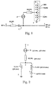
- Fig. 1 shows one resonator of the duplex filter, connected to a bandstop circuit which attenuates the signal causing spurious response when the local oscillator injection is located on the upper side.
- the signal frequency causing spurious response is located by half of the intermediate frequency above the receiving frequency.
- the circuit is formed from a helical resonator Res, a capacitance diode D and a microstrip MLIN2 in series therewith.
- the microstrip conductor is at one end coupled to the resonator e.g. by tapping at point 3 with the helical resonator Res, which is thus divided into two parts, TLIN1 and TLIN2 and coupled to the diodes D at its other end.
- the other end of the diode is coupled to point 1 in the main signal circuit of the Rx branch in the duplex filter.
- the coupling has been positioned for the last component in the Rx branch, so that the circuit is connected to the Rx gate of the filter.
- the function of the capacitor C is to prevent the access of direct voltage to the duplex filter proper.
- a signal to be received from the antenna is fed via the other resonators (not shown) of the duplex filter through the microstrip MLIN1 to point 1, which also serves as the output gate for the Rx of the filter.
- Endeavours are made to dimension the circuit so that the series resonance frequency of a resonator connected as band stop circuit can be controlled from 970 MHz to 990 MHz. While connected to the filter the band stop circuit increases the attenuation of the spurious response signal in the upper part of the pass band, whereby spurious response in the receiver are reduced.
- the circuit can be shown in a more clarified form, as in Fig. 2. Assume that at 940 MHz frequency the reactance of TLIN1 is j*59 ohms and the reactance of TLIN2 is j*413 ohms.
- the capacitance of the varactor varies in the range from 27 pF to 3 pF, that is, from -j*6 ohms to -j*56 ohms. It is known in the art that the reactance of a resonance circuit, such as a helical resonator Res, is capacitive above its resonance frequency.
- a series resonance is provided by connecting from point 3 a series connection formed by the microstrip conductor MLIN2 and the capacitance diode D against the earth.
- the capacitive reactance of the resonator Res at that frequency is e.g. 56.1 ohms, whereby the microstrip MLIN2 and the reactance of the series connection of the capacitance diode must be of equal magnitude but of opposite sign in reactance, that is, 56.1 ohms inductive.
- the inductive reactance of the microstrip is 56.1 ohms, i.e. 62.17 ohms, being about 10 nH when calculated in inductance.
- the resonance circuit is in series resonance at 970 MHz.
- the series resonance frequency can be smoothly controlled by changing the capacitance of the capacitance diode, i.e. by varying the magnitude of the direct voltage across the diode.
- the magnitude of the capacitance of the varactor is about 3 pF, a desired 990 MHz is obtained for the series resonance frequency.
- Fig. 3 shows the penetration curve of the Rx branch of a duplex filter intended for the NMT radio phone system using the embodiment of Fig. 1.
- a controllable resonator has been positioned at the Rx end of a filter as far as possible from the antenna gate in which high transmitter power affects the duplex filter. This results in the transmitter signal being attenuated in the Rx branch of the duplex filter by about 50 dB prior to the controllable circuit operated In accordance with the invention.
- the high frequency signal visible in the varactor is very low level, thus having no effect on the behaviour of the circuit to be controlled. If the circuit to be controlled were positioned in the proximity of the antenna gate, the operation of the circuit would be completely disturbed.
- the frequency response of the filter is as shown in curve 1. It is found that the circuit creates about 10 dB attenuation in the range 957.5 MHz to 960 MHz.
- the series resonance frequency of the circuit is at point A.
- the spurious response signal generated in the mixer of the radio telephone can be effectively attenuated without making any changes in the other components, and as a result, significantly improves the performance of the apparatus.
- the frequency of the spurious response signal is lower by half of the intermediate frequency than the received frequency.
- a circuit such as in Fig. 4 can be used.
- the same references are used as in Fig. 1.
- a zero point is now set (series resonance frequency) below the receiving band. This is carried out by having in addition to the inductance MLIN2, a capacitor C2 is used in the circuit.
- the DC voltage used for controlling the capacitance of the varactor is supplied to the circuit via resistor R. The series resonance frequency of the circuit is thus produced below the receiving band.
- amplitude response of a circuit as in Fig. 4 is shown on 10 dB scale in Fig. 5. As can be seen, zero is now at about 915 Mhz frequency, and the frequencies adjacent to said frequency are sufficiently attenuated not to cause spurious response.
- the series resonance frequency may, in fact, be controlled steplessly, but it is simple to use two direct voltage states only for the control voltage of the capacitance.
- the direct voltage needed by the varactor can be fed via the Rx signal gate, whereby the mechanical structure of the filter remains externally unchanged and no separate gate is needed for supplying direct voltage.
- a separate gate intended for supplying DC voltage may also be used.
- the frequency of the zero point to be controlled can be changed also at the desired frequencies other than at frequencies which cause a spurious response.
- e.g. 980 - 1005 MHz can be sized toe form the control range in which range the local oscillator of a radio telephone operates when using a 45 MHz intermediate frequency.
- the leakage of the local oscillator into the antenna gate of the apparatus can be prevented by setting the series resonance frequency at the local oscillator frequency used each time.
- a so-called mirror frequency range can be selected, which in the NMT occurs in the range 1025 to 1050 MHz, and therethrough improve the mirror frequency attenuation remarkably.
- Helical resonators are used in the examples, but it is equally possible to use LC circuit, coaxial resonator, strip line or equivalent resonator, neither is it necessary to limit the implementation to the examples described above.
- the circuit can be implemented in a number of different ways while remaining within the protective scope of the claims.
- the filter need not be a duplex filter, either, and the scope of the invention is appropriate for use in association with any radio frequency filter.
Landscapes
- Noise Elimination (AREA)
- Control Of Motors That Do Not Use Commutators (AREA)
- Superheterodyne Receivers (AREA)
- Mobile Radio Communication Systems (AREA)
- Filters And Equalizers (AREA)
Description
- The present invention relates to a radio frequency filter, In particular a filter for attenuating spurious responses from a receiver mixer of a radio telephone.
- In radio telephones, a received radio signal is usually coupled from an antenna to a duplex filter from where it is passed through a first amplifier located in the front end of the receiver. The received signal is then passed through a fixed bandpass filter to a first mixer where it is mixed with a local oscillator frequency, to yield an intermediate frequency which is filtered from the general mixer response. The intermediate frequency signal is amplified prior to be taken to a second mixer. To reduce component costs and to simplify the basic structure of a receiver, it would be advantageous to select a low intermediate frequency. However, the selection of a low intermediate frequency, may cause difficulties not solvable by means of fixed filters. For example, the attenuation of signals such as local oscillator signals, which are at a distance of the intermediate frequency from a signal to be received and mirror frequency signals, which are at twice the distance of the intermediate frequency from the receiving band, may be difficult to achieve.
- A spurious response signal is generally higher than the received Rf signal by half of the intermediate frequency if the local oscillator injection frequency is located on the upper side of the received signal (the local oscillator frequency is higher than the frequency to be received). Conversely it is half of the intermediate frequency lower than the received Rf signal if the local oscillator injection signal is located on the lower side of the received signal (the local oscillator frequency is lower than the frequency to be received).
- When the intermediate frequency is sufficiently high relative to the receiving band, i.e. higher by at least twice the width of the reception band, the frequency components generating a spurious response can be filtered by means of fixed filters in the high frequency components of the receiver. For this purpose, the first intermediate frequency is in general selected to be sufficiently high, as described above, although the components to be used are more difficult to produce and therefore more expensive. For example, in the NMT radio telephone system, the width of the receiving band is 25 MHz and the intermediate frequency over 50 MHz. e.g. 87 MHz. In certain radio telephone systems attenuation required in the telephone to overcome the spurious response is so high that the receiver will not operate according to the specifications of the system without a separate system specifically to attenuate the spurious response cause by the harmonic components.
- The problem related to spurious response particularly arises in the upper end of the receiving band. When a receiver is listening at the lower end of the receiving band, the spurious response frequencies are created in the upper end of the receiving band where the front end filters are not provided with any attenuation. If in said frequency range a powerful signal occurs, a harmful spurious response is generated in the mixer. In the worst instance, this inhibits the entire listening or understanding of the desired received signal. If, as in the above example, the width of the receiving band in an NMT phone is 25 MHz and, if the intermediate frequency is below 2*25 MHz, i.e. below 50 MHz, a detrimental spurious response is created, the frequency of which spurious signal being located in the upper end of the receiving band. When the signal frequency to be received is located at the upper end of the receiving frequency band, the frequency created by the spurious response moves outside the receiving band, and the fixed filters prior to the mixer are capable of removing the spurious response. Thus, problems arise particularly when the receiver is tuned to be in the lower range of the receiving band and the signals causing spurious response are located in the upper range of the receiving band.
- The generation of a spurious response in a mixer is easiest to avoid by selecting a sufficient intermediate frequency, i.e. twice the band width of the receiver band, whereby the signal creating spurious response will not occur in the listening range of the receiver.
- Signals creating a spurious response may be reduced by using a controllable filter after the RF amplifier, however, such a filter is currently not commercially available.
- The properties of the mixer may also be enhanced or improved but more expensive filters could be used. A separate suction filter can be used which is coupled between the RF signal route and the earth of the apparatus prior to the mixer of the receiver. Such a suction filter like that is disclosed in patent FI-86014. Therein, the suction filter is a resonator, e.g. a helical resonator, the resonance frequency whereof being controllable with the control voltage of a capacitance diode included in the circuit. The value of the control voltage changes with a change in receiving channel in that together with the increasing frequency of the receiving channel, the resonance frequency of the resonator increases.
- The Finnish patent application FI-902149 also discloses a useful circuit. It includes a resonance circuit coupled before the intermediate amplifier between the signal route and the earth of the circuit. The resonance circuit is at series resonance at a frequency half of the intermediate frequency, whereby a signal of said frequency is strongly attenuated, and in parallel resonance when the frequency is an intermediate frequency so that the attenuation of a signal at said frequency is not significant. The resonator circuit comprises an inductance and capacitance connected in parallel, and a series capacitance. The circuit is at series resonance at a frequency half of the intermediate frequency, e.g. at 22.5 MHz frequency when using a 45 MHz intermediate frequency. Hereby, the impedance of the resonance circuit is very low, and the 22.5 MHz frequency component is powerfully attenuated before the amplifier and the other harmonics visible in the output of the amplifier is therefore so small that the spurious response requirement specified by the specification is met. The same resonance circuit is in parallel resonance at an intermediate frequency, e.g. 45 MHz, so that the impedance thereof is very high, thus not attenuating the intermediate frequency signal. Said design is appropriate for use when a phone is designed to meet a given specification. With a changed specification, the resonance circuit has to be dimensioned once again. It is furthermore to be noted that the circuit is intended for a signal of intermediate frequency.
- In
publication EP 0 472 319 is presented a tunable bandpass filter comprising a plurality of resonators. The circuit, which produces the tunable stop band, is connected to the "hot" end of a resonator, and consists wholly of discrete components. A disadvantage of the structure is, that it needs plenty of additional components. Furthermore connecting the capacitance diodes to the end of resonator, in which the strength of electric field is at its height, causes a danger of hazardous intermodulation in the diodes. - A duplex filter comprising a transmitter filter Tx coupled to the transmitter branch and a receiver filter coupled to the receiver branch. The filters can be of bandstop or bandpass type, or combinations thereof, typically implemented with transmission line resonators, such as coaxial or helical resonators.
- In accordance with the present invention there is provided a radio frequency band pass filter comprising a plurality of resonators, and having tuning means to shape its frequency response, said tuning means being connected to a tapping point of at least one of said resonators to change at certain frequency said resonator to a serial resonance circuit, whereby said tapping point divides the resonator into two parts.
- In a circuit in accordance with the present invention, one of the resonators in a Rx part of a duplex filter has been coupled into a bandstop type circuit and positioned as far as possible from the antenna gate. The circuit operates at radio frequency and it is characterized in that it passes the signals above and below the series resonance frequency thereof nearly unattenuated. It has been so implemented that the resonator has been divided into two parts. The point between the parts has been coupled via a capacitance diode and an inductance in series therewith to the main circuit of the duplex filter. A signal to be received from the antenna is fed via the other resonators of the filter through an adaption element, such as microstrip, to a point whereto the circuit of the invention has been coupled and which may also at the same time form the output gate for the Rx of the filter.
- The circuit has been so sized that the series resonance of the bandstop circuit is located above the receiving band and the frequency of the circuit can be controlled. While in the series resonance, the circuit attenuates the resonance frequency signal, and by positioning the zero point by half of the intermediate frequency above the receiving frequency (in case of an upper local oscillator injection) or below the receiving frequency (in case of lower local oscillator injection), the signal generating spurious response can be attenuated as early as in the duplex filter.
- A further advantage of the present invention is that no or few extra circuit components are required in the filter, thereby reducing costs and manufacturing complexity.
- Specific embodiments of the invention is described in detail by way of example only, and with the aid of the accompanying drawings, in which:
- Fig. 1 presents a principle picture of the circuit of the invention,
- Fig. 2 shows more clarified the circuit of Fig. 1,
- Fig. 3 presents the amplitude response of a duplex filter when using the circuit of Fig. 1,
- Fig. 4 is a principle figure of a circuit according to second embodiment, and
- Fig. 5 shows the frequency response of the circuit of Fig. 4.
-
- Fig. 1 shows one resonator of the duplex filter, connected to a bandstop circuit which attenuates the signal causing spurious response when the local oscillator injection is located on the upper side. The signal frequency causing spurious response is located by half of the intermediate frequency above the receiving frequency. The circuit is formed from a helical resonator Res, a capacitance diode D and a microstrip MLIN2 in series therewith. The microstrip conductor is at one end coupled to the resonator e.g. by tapping at
point 3 with the helical resonator Res, which is thus divided into two parts, TLIN1 and TLIN2 and coupled to the diodes D at its other end. The other end of the diode is coupled topoint 1 in the main signal circuit of the Rx branch in the duplex filter. In the example shown in the figure, the coupling has been positioned for the last component in the Rx branch, so that the circuit is connected to the Rx gate of the filter. The function of the capacitor C is to prevent the access of direct voltage to the duplex filter proper. A signal to be received from the antenna is fed via the other resonators (not shown) of the duplex filter through the microstrip MLIN1 topoint 1, which also serves as the output gate for the Rx of the filter. - Endeavours are made to dimension the circuit so that the series resonance frequency of a resonator connected as band stop circuit can be controlled from 970 MHz to 990 MHz. While connected to the filter the band stop circuit increases the attenuation of the spurious response signal in the upper part of the pass band, whereby spurious response in the receiver are reduced.
- The circuit can be shown in a more clarified form, as in Fig. 2. Assume that at 940 MHz frequency the reactance of TLIN1 is j*59 ohms and the reactance of TLIN2 is j*413 ohms. The capacitance of the varactor varies in the range from 27 pF to 3 pF, that is, from -j*6 ohms to -j*56 ohms. It is known in the art that the reactance of a resonance circuit, such as a helical resonator Res, is capacitive above its resonance frequency. Hereby, a series resonance is provided by connecting from point 3 a series connection formed by the microstrip conductor MLIN2 and the capacitance diode D against the earth. When attenuation is desired to be at 970 MHz, the capacitive reactance of the resonator Res at that frequency is e.g. 56.1 ohms, whereby the microstrip MLIN2 and the reactance of the series connection of the capacitance diode must be of equal magnitude but of opposite sign in reactance, that is, 56.1 ohms inductive. This is implemented when the inductive reactance of the microstrip is 56.1 ohms, i.e. 62.17 ohms, being about 10 nH when calculated in inductance. Hereby, the resonance circuit is in series resonance at 970 MHz.
- The series resonance frequency can be smoothly controlled by changing the capacitance of the capacitance diode, i.e. by varying the magnitude of the direct voltage across the diode. When the magnitude of the capacitance of the varactor is about 3 pF, a desired 990 MHz is obtained for the series resonance frequency. By selecting an appropriate diode with a wide capacitance range, the series resonance frequency can be varied over an even wider range.
- Fig. 3 shows the penetration curve of the Rx branch of a duplex filter intended for the NMT radio phone system using the embodiment of Fig. 1. A controllable resonator has been positioned at the Rx end of a filter as far as possible from the antenna gate in which high transmitter power affects the duplex filter. This results in the transmitter signal being attenuated in the Rx branch of the duplex filter by about 50 dB prior to the controllable circuit operated In accordance with the invention. Thus, the high frequency signal visible in the varactor is very low level, thus having no effect on the behaviour of the circuit to be controlled. If the circuit to be controlled were positioned in the proximity of the antenna gate, the operation of the circuit would be completely disturbed. When the varactor is unbiased (control voltage 0 V), the frequency response of the filter is as shown in
curve 1. It is found that the circuit creates about 10 dB attenuation in the range 957.5 MHz to 960 MHz. The series resonance frequency of the circuit is at point A. - When a direct voltage of a few volts is supplied to the varactor, the series resonance frequency of the resonator increases and moves to point B, and the frequency response of the Rx branch of the filter is as shown in
curve 2. The zero point moves upwards in frequency. - Due to the form of coupling used in the present invention , no changes need be made in the mixer of the radio telephone due to of spurious responses. Thus, using a design in accordance with the invention, the spurious response signal generated in the mixer of the radio telephone can be effectively attenuated without making any changes in the other components, and as a result, significantly improves the performance of the apparatus.
- If the local oscillator injection is located on the lower side (the received frequency is higher than the local oscillator frequency), the frequency of the spurious response signal is lower by half of the intermediate frequency than the received frequency. For such a situation, a circuit such as in Fig. 4 can be used. When applicable, the same references are used as in Fig. 1. A zero point is now set (series resonance frequency) below the receiving band. This is carried out by having in addition to the inductance MLIN2, a capacitor C2 is used in the circuit. The DC voltage used for controlling the capacitance of the varactor is supplied to the circuit via resistor R. The series resonance frequency of the circuit is thus produced below the receiving band.
- The amplitude response of a circuit as in Fig. 4 is shown on 10 dB scale in Fig. 5. As can be seen, zero is now at about 915 Mhz frequency, and the frequencies adjacent to said frequency are sufficiently attenuated not to cause spurious response.
- By positioning the attenuation circuit of a signal causing spurious response in association with the duplex filter, no extra circuits need be placed in the receiver branch, as is the case in state of the art designs.
- The series resonance frequency may, in fact, be controlled steplessly, but it is simple to use two direct voltage states only for the control voltage of the capacitance. When a controllable resonator according to the invention is used in the filter, the direct voltage needed by the varactor can be fed via the Rx signal gate, whereby the mechanical structure of the filter remains externally unchanged and no separate gate is needed for supplying direct voltage. If desired, a separate gate intended for supplying DC voltage may also be used.
- By appropriate sizing of the components of the circuit to be controlled, the frequency of the zero point to be controlled can be changed also at the desired frequencies other than at frequencies which cause a spurious response. For instance, e.g. 980 - 1005 MHz can be sized toe form the control range in which range the local oscillator of a radio telephone operates when using a 45 MHz intermediate frequency. The leakage of the local oscillator into the antenna gate of the apparatus can be prevented by setting the series resonance frequency at the local oscillator frequency used each time. Likewise, for the operation range, a so-called mirror frequency range can be selected, which in the NMT occurs in the range 1025 to 1050 MHz, and therethrough improve the mirror frequency attenuation remarkably.
- Helical resonators are used in the examples, but it is equally possible to use LC circuit, coaxial resonator, strip line or equivalent resonator, neither is it necessary to limit the implementation to the examples described above. The circuit can be implemented in a number of different ways while remaining within the protective scope of the claims. The filter need not be a duplex filter, either, and the scope of the invention is appropriate for use in association with any radio frequency filter.
Claims (11)
- A radio frequency band pass filter comprising a plurality of resonators, and having tuning means to shape its frequency response, characterised in that said tuning means are connected to a tapping point (3) of at least one of said resonators to change, if necessary, at certain frequency (A; B) said resonator to a serial resonance circuit, whereby said tapping point divides the resonator into two parts.
- Radio frequency filter according to claim 1, characterised in thatsaid tuning means comprise a series connection of an inductive element (MLIN2) and a capacitance diode (D), which is controlled by means of a direct voltage control signal (V+), andat a certain first value of the direct voltage control signal the resonance frequency (A) of said serial resonance circuit is arranged to be within the pass band of said filter.
- Radio frequency filter according to claim 2, characterised in thatsaid one of the resonator is a transmission line resonator (RES),one end of said series connection is connected to said tapping point (3) that divides the transmission line resonator into two parts (TLIN1, TLIN2),the other end of said series connection is connected to the output port (1) of the radio frequency filter.
- Radio frequency filter according to claim 3, characterised in that the reactance of said series connection is arranged so that at said first value of said direct voltage control signal said series resonance frequency is located in upper region of the pass band of the filter.
- Radio frequency filter according to claim 3, characterised in that the reactance of said series connection is arranged so that at said first value of said direct voltage control signal said series resonance frequency is located in lower region of the pass band of the filter.
- Radio frequency filter according to claim 3, characterised in that said inductive element (MLIN2) is a strip line or a coil.
- Radio frequency filter according to claim 2, characterised in that said direct voltage control signal (V+) is fed to an output port (1) of the radio frequency filter.
- A radio frequency filter according to claim 7, characterised in that said tuning means further comprisea resistor (R) to couple said direct voltage control signal (V+) from the output port (1) to the cathode (2) of the capacitance diode (D) anda capacitor (C2) in series with the capacitance diode (D) to couple the series resonance circuit to the output port (1) of the radio frequency filter.
- Radio frequency filter according to claim 1, characterised in that it is a duplex filter comprising a transmitting branch and a receiving branch, and said one of the resonators is located in the receiving branch of the radio frequency filter.
- Radio frequency filter according to claim 9, characterised in that the resonance frequency of said serial resonance circuit is the same as a local oscillator frequency of said radio receiver.
- Radio frequency filter according to claim 9, characterised in that it comprises an antenna port for connecting it to the antenna of said radio receiver, an output port (1) for connecting it to the receiver circuit of said radio receiver, and a number of transmission line resonators between said antenna port and said output port, whereby said one of the resonators comprises the transmission line resonator (RES) located distally from said antenna port in the direction of said output port (1).
Applications Claiming Priority (2)
| Application Number | Priority Date | Filing Date | Title |
|---|---|---|---|
| FI933988 | 1993-09-10 | ||
| FI933988A FI110148B (en) | 1993-09-10 | 1993-09-10 | Multi-resonator radio frequency filter |
Publications (2)
| Publication Number | Publication Date |
|---|---|
| EP0643481A1 EP0643481A1 (en) | 1995-03-15 |
| EP0643481B1 true EP0643481B1 (en) | 2002-07-24 |
Family
ID=8538571
Family Applications (1)
| Application Number | Title | Priority Date | Filing Date |
|---|---|---|---|
| EP94306650A Expired - Lifetime EP0643481B1 (en) | 1993-09-10 | 1994-09-09 | Radio frequency filter |
Country Status (5)
| Country | Link |
|---|---|
| US (1) | US5717368A (en) |
| EP (1) | EP0643481B1 (en) |
| JP (1) | JPH07170204A (en) |
| DE (1) | DE69431022T2 (en) |
| FI (1) | FI110148B (en) |
Families Citing this family (44)
| Publication number | Priority date | Publication date | Assignee | Title |
|---|---|---|---|---|
| FI110148B (en) * | 1993-09-10 | 2002-11-29 | Filtronic Lk Oy | Multi-resonator radio frequency filter |
| WO2002037708A2 (en) | 2000-11-03 | 2002-05-10 | Paratek Microwave, Inc. | Method of channel frequency allocation for rf and microwave duplexers |
| SE520112C2 (en) * | 2000-12-27 | 2003-05-27 | Allgon Ab | Method and system for tuning a radio filter |
| WO2006000650A1 (en) | 2004-06-28 | 2006-01-05 | Pulse Finland Oy | Antenna component |
| FI20055420A0 (en) * | 2005-07-25 | 2005-07-25 | Lk Products Oy | Adjustable multi-band antenna |
| FI119009B (en) * | 2005-10-03 | 2008-06-13 | Pulse Finland Oy | Multiple-band antenna |
| FI118782B (en) | 2005-10-14 | 2008-03-14 | Pulse Finland Oy | Adjustable antenna |
| FI119577B (en) * | 2005-11-24 | 2008-12-31 | Pulse Finland Oy | The multiband antenna component |
| US8618990B2 (en) | 2011-04-13 | 2013-12-31 | Pulse Finland Oy | Wideband antenna and methods |
| US10211538B2 (en) | 2006-12-28 | 2019-02-19 | Pulse Finland Oy | Directional antenna apparatus and methods |
| FI20075269A0 (en) * | 2007-04-19 | 2007-04-19 | Pulse Finland Oy | Method and arrangement for antenna matching |
| FI120427B (en) | 2007-08-30 | 2009-10-15 | Pulse Finland Oy | Adjustable multiband antenna |
| KR101610956B1 (en) * | 2009-10-01 | 2016-04-08 | 삼성전자주식회사 | Wideband rf receiver in wireless communications systmem and control method therefor |
| FI20096134A0 (en) | 2009-11-03 | 2009-11-03 | Pulse Finland Oy | Adjustable antenna |
| FI20096251A0 (en) | 2009-11-27 | 2009-11-27 | Pulse Finland Oy | MIMO antenna |
| US8847833B2 (en) * | 2009-12-29 | 2014-09-30 | Pulse Finland Oy | Loop resonator apparatus and methods for enhanced field control |
| FI20105158A7 (en) | 2010-02-18 | 2011-08-19 | Pulse Finland Oy | ANTENNA EQUIPPED WITH SHELL RADIATOR |
| US9406998B2 (en) | 2010-04-21 | 2016-08-02 | Pulse Finland Oy | Distributed multiband antenna and methods |
| FI20115072A0 (en) | 2011-01-25 | 2011-01-25 | Pulse Finland Oy | Multi-resonance antenna, antenna module and radio unit |
| US9673507B2 (en) | 2011-02-11 | 2017-06-06 | Pulse Finland Oy | Chassis-excited antenna apparatus and methods |
| US8648752B2 (en) | 2011-02-11 | 2014-02-11 | Pulse Finland Oy | Chassis-excited antenna apparatus and methods |
| US8866689B2 (en) | 2011-07-07 | 2014-10-21 | Pulse Finland Oy | Multi-band antenna and methods for long term evolution wireless system |
| US9450291B2 (en) | 2011-07-25 | 2016-09-20 | Pulse Finland Oy | Multiband slot loop antenna apparatus and methods |
| US9123990B2 (en) | 2011-10-07 | 2015-09-01 | Pulse Finland Oy | Multi-feed antenna apparatus and methods |
| US9531058B2 (en) | 2011-12-20 | 2016-12-27 | Pulse Finland Oy | Loosely-coupled radio antenna apparatus and methods |
| US9484619B2 (en) | 2011-12-21 | 2016-11-01 | Pulse Finland Oy | Switchable diversity antenna apparatus and methods |
| US8988296B2 (en) | 2012-04-04 | 2015-03-24 | Pulse Finland Oy | Compact polarized antenna and methods |
| US9979078B2 (en) | 2012-10-25 | 2018-05-22 | Pulse Finland Oy | Modular cell antenna apparatus and methods |
| US10069209B2 (en) | 2012-11-06 | 2018-09-04 | Pulse Finland Oy | Capacitively coupled antenna apparatus and methods |
| US9647338B2 (en) | 2013-03-11 | 2017-05-09 | Pulse Finland Oy | Coupled antenna structure and methods |
| US10079428B2 (en) | 2013-03-11 | 2018-09-18 | Pulse Finland Oy | Coupled antenna structure and methods |
| US9634383B2 (en) | 2013-06-26 | 2017-04-25 | Pulse Finland Oy | Galvanically separated non-interacting antenna sector apparatus and methods |
| US9680212B2 (en) | 2013-11-20 | 2017-06-13 | Pulse Finland Oy | Capacitive grounding methods and apparatus for mobile devices |
| US9590308B2 (en) | 2013-12-03 | 2017-03-07 | Pulse Electronics, Inc. | Reduced surface area antenna apparatus and mobile communications devices incorporating the same |
| US9893715B2 (en) | 2013-12-09 | 2018-02-13 | Shure Acquisition Holdings, Inc. | Adaptive self-tunable antenna system and method |
| US9350081B2 (en) | 2014-01-14 | 2016-05-24 | Pulse Finland Oy | Switchable multi-radiator high band antenna apparatus |
| US9948002B2 (en) | 2014-08-26 | 2018-04-17 | Pulse Finland Oy | Antenna apparatus with an integrated proximity sensor and methods |
| US9973228B2 (en) | 2014-08-26 | 2018-05-15 | Pulse Finland Oy | Antenna apparatus with an integrated proximity sensor and methods |
| US9722308B2 (en) | 2014-08-28 | 2017-08-01 | Pulse Finland Oy | Low passive intermodulation distributed antenna system for multiple-input multiple-output systems and methods of use |
| JP6442766B2 (en) | 2014-12-11 | 2018-12-26 | 富士通コネクテッドテクノロジーズ株式会社 | Wireless communication apparatus, wireless communication method, and wireless communication program |
| KR102324960B1 (en) | 2015-06-25 | 2021-11-12 | 삼성전자 주식회사 | Communication device and electronic device including the same |
| US9906260B2 (en) | 2015-07-30 | 2018-02-27 | Pulse Finland Oy | Sensor-based closed loop antenna swapping apparatus and methods |
| JP2020005185A (en) * | 2018-06-29 | 2020-01-09 | ルネサスエレクトロニクス株式会社 | Communication device |
| CN113851845B (en) * | 2021-10-13 | 2024-01-26 | 中国信息通信研究院 | An integrated filter duplex antenna that suppresses in-band signals |
Family Cites Families (14)
| Publication number | Priority date | Publication date | Assignee | Title |
|---|---|---|---|---|
| GB960280A (en) * | 1961-06-07 | 1964-06-10 | Marconi Co Ltd | Improvements in or relating to variable reactance and like arrangements |
| US3733608A (en) * | 1971-12-09 | 1973-05-15 | Motorola Inc | Circuit for coupling radio receiver and radio transmitter to a common antenna for duplex operation |
| IT1074089B (en) * | 1976-12-16 | 1985-04-17 | Sits Soc It Telecom Siemens | BAND-REJECT FILTER FOR TELECOMMUNICATIONS SYSTEMS |
| US4426630A (en) * | 1981-12-28 | 1984-01-17 | Rockwell International Corporation | Electronically tunable band reject filter |
| US4459571A (en) * | 1982-12-20 | 1984-07-10 | Motorola, Inc. | Varactor-tuned helical resonator filter |
| FR2565438B1 (en) * | 1984-05-30 | 1989-09-22 | Cepe | DIELECTRIC FILTER WITH VARIABLE CENTRAL FREQUENCY. |
| US4682131A (en) * | 1985-06-07 | 1987-07-21 | Motorola Inc. | High-Q RF filter with printed circuit board mounting temperature compensated and impedance matched helical resonators |
| US4662001A (en) * | 1985-08-15 | 1987-04-28 | Zenith Electronics Corporation | Tunable notch filter for image frequency and conducted local oscillator leakage rejection |
| JPS6489709A (en) * | 1987-09-30 | 1989-04-04 | Toshiba Corp | Band width variable circuit |
| US4799034A (en) * | 1987-10-26 | 1989-01-17 | General Instrument Corporation | Varactor tunable coupled transmission line band reject filter |
| US5065453A (en) * | 1989-03-20 | 1991-11-12 | General Electric Company | Electrically-tunable bandpass filter |
| GB2247125B (en) * | 1990-08-16 | 1995-01-11 | Technophone Ltd | Tunable bandpass filter |
| US5107233A (en) * | 1990-10-15 | 1992-04-21 | Hewlett-Packard Company | Amplitude correction of field coupled varactor tuned filters |
| FI110148B (en) * | 1993-09-10 | 2002-11-29 | Filtronic Lk Oy | Multi-resonator radio frequency filter |
-
1993
- 1993-09-10 FI FI933988A patent/FI110148B/en not_active IP Right Cessation
-
1994
- 1994-09-09 EP EP94306650A patent/EP0643481B1/en not_active Expired - Lifetime
- 1994-09-09 DE DE69431022T patent/DE69431022T2/en not_active Expired - Fee Related
- 1994-09-12 JP JP6217365A patent/JPH07170204A/en active Pending
-
1996
- 1996-11-14 US US08/746,675 patent/US5717368A/en not_active Expired - Fee Related
Also Published As
| Publication number | Publication date |
|---|---|
| FI110148B (en) | 2002-11-29 |
| FI933988A0 (en) | 1993-09-10 |
| DE69431022D1 (en) | 2002-08-29 |
| EP0643481A1 (en) | 1995-03-15 |
| US5717368A (en) | 1998-02-10 |
| FI933988L (en) | 1995-03-11 |
| DE69431022T2 (en) | 2003-03-13 |
| JPH07170204A (en) | 1995-07-04 |
Similar Documents
| Publication | Publication Date | Title |
|---|---|---|
| US5717368A (en) | Varactor tuned helical resonator for use with duplex filter | |
| US5227748A (en) | Filter with electrically adjustable attenuation characteristic | |
| DE69517348T2 (en) | Arrangement for separating transmission and reception signals in a transceiver | |
| EP0570184B1 (en) | A filter used as transmit-receive switch | |
| US5627502A (en) | Resonator filter with variable tuning | |
| US5267234A (en) | Radio transceiver with duplex and notch filter | |
| US4662001A (en) | Tunable notch filter for image frequency and conducted local oscillator leakage rejection | |
| US10340874B2 (en) | Filter circuit, RF front end circuit, and communication apparatus | |
| EP0820661B1 (en) | Tv/fm receiver for multimedia applications | |
| US5963842A (en) | Satellite broadcasting receiving tuner | |
| CA1237480A (en) | Tracking image frequency trap | |
| US5262741A (en) | Attenuator for high-frequency signal | |
| JPS639303A (en) | Microwave filter and transmitting/receiving equipment using same | |
| US5978663A (en) | Antenna tuning circuit | |
| CA2659025C (en) | Tunable narrow band filter | |
| US20030119455A1 (en) | Transmitting/receiving switch and portable terminal unit | |
| US5977835A (en) | Method and circuit arrangement for reducing passband ripple of a bandpass filter | |
| EP0404225A2 (en) | Radio receiver | |
| KR20040083494A (en) | Television tuner and printed circuit board used therein | |
| KR960008981B1 (en) | Filter circuit for attenuating high frequency signals | |
| GB2276786A (en) | A voltage controlled filter | |
| KR910003172Y1 (en) | Input filter circuit for wire tv tuner | |
| KR100274047B1 (en) | TV signal input circuit | |
| EP0614243A1 (en) | Electrical filter | |
| JPH08330807A (en) | Dielectric filter |
Legal Events
| Date | Code | Title | Description |
|---|---|---|---|
| PUAI | Public reference made under article 153(3) epc to a published international application that has entered the european phase |
Free format text: ORIGINAL CODE: 0009012 |
|
| AK | Designated contracting states |
Kind code of ref document: A1 Designated state(s): CH DE DK FR GB LI |
|
| 17P | Request for examination filed |
Effective date: 19950915 |
|
| 17Q | First examination report despatched |
Effective date: 19990105 |
|
| RAP1 | Party data changed (applicant data changed or rights of an application transferred) |
Owner name: FILTRONIC LK OY |
|
| GRAG | Despatch of communication of intention to grant |
Free format text: ORIGINAL CODE: EPIDOS AGRA |
|
| GRAG | Despatch of communication of intention to grant |
Free format text: ORIGINAL CODE: EPIDOS AGRA |
|
| GRAG | Despatch of communication of intention to grant |
Free format text: ORIGINAL CODE: EPIDOS AGRA |
|
| GRAH | Despatch of communication of intention to grant a patent |
Free format text: ORIGINAL CODE: EPIDOS IGRA |
|
| RIN1 | Information on inventor provided before grant (corrected) |
Inventor name: NIIRANEN, ERKKI |
|
| GRAH | Despatch of communication of intention to grant a patent |
Free format text: ORIGINAL CODE: EPIDOS IGRA |
|
| GRAA | (expected) grant |
Free format text: ORIGINAL CODE: 0009210 |
|
| AK | Designated contracting states |
Kind code of ref document: B1 Designated state(s): CH DE DK FR GB LI |
|
| PG25 | Lapsed in a contracting state [announced via postgrant information from national office to epo] |
Ref country code: LI Free format text: LAPSE BECAUSE OF FAILURE TO SUBMIT A TRANSLATION OF THE DESCRIPTION OR TO PAY THE FEE WITHIN THE PRESCRIBED TIME-LIMIT Effective date: 20020724 Ref country code: CH Free format text: LAPSE BECAUSE OF FAILURE TO SUBMIT A TRANSLATION OF THE DESCRIPTION OR TO PAY THE FEE WITHIN THE PRESCRIBED TIME-LIMIT Effective date: 20020724 |
|
| REG | Reference to a national code |
Ref country code: GB Ref legal event code: FG4D |
|
| REG | Reference to a national code |
Ref country code: CH Ref legal event code: EP |
|
| REF | Corresponds to: |
Ref document number: 69431022 Country of ref document: DE Date of ref document: 20020829 |
|
| PG25 | Lapsed in a contracting state [announced via postgrant information from national office to epo] |
Ref country code: DK Free format text: LAPSE BECAUSE OF FAILURE TO SUBMIT A TRANSLATION OF THE DESCRIPTION OR TO PAY THE FEE WITHIN THE PRESCRIBED TIME-LIMIT Effective date: 20021024 |
|
| ET | Fr: translation filed | ||
| REG | Reference to a national code |
Ref country code: CH Ref legal event code: PL |
|
| PLBE | No opposition filed within time limit |
Free format text: ORIGINAL CODE: 0009261 |
|
| STAA | Information on the status of an ep patent application or granted ep patent |
Free format text: STATUS: NO OPPOSITION FILED WITHIN TIME LIMIT |
|
| 26N | No opposition filed |
Effective date: 20030425 |
|
| PGFP | Annual fee paid to national office [announced via postgrant information from national office to epo] |
Ref country code: GB Payment date: 20030903 Year of fee payment: 10 |
|
| PGFP | Annual fee paid to national office [announced via postgrant information from national office to epo] |
Ref country code: FR Payment date: 20030909 Year of fee payment: 10 |
|
| PGFP | Annual fee paid to national office [announced via postgrant information from national office to epo] |
Ref country code: DE Payment date: 20030918 Year of fee payment: 10 |
|
| PG25 | Lapsed in a contracting state [announced via postgrant information from national office to epo] |
Ref country code: GB Free format text: LAPSE BECAUSE OF NON-PAYMENT OF DUE FEES Effective date: 20040909 |
|
| PG25 | Lapsed in a contracting state [announced via postgrant information from national office to epo] |
Ref country code: DE Free format text: LAPSE BECAUSE OF NON-PAYMENT OF DUE FEES Effective date: 20050401 |
|
| GBPC | Gb: european patent ceased through non-payment of renewal fee |
Effective date: 20040909 |
|
| PG25 | Lapsed in a contracting state [announced via postgrant information from national office to epo] |
Ref country code: FR Free format text: LAPSE BECAUSE OF NON-PAYMENT OF DUE FEES Effective date: 20050531 |
|
| REG | Reference to a national code |
Ref country code: FR Ref legal event code: ST |