EP0636989B1 - Multi-channel data receiver system - Google Patents
Multi-channel data receiver system Download PDFInfo
- Publication number
- EP0636989B1 EP0636989B1 EP94111603A EP94111603A EP0636989B1 EP 0636989 B1 EP0636989 B1 EP 0636989B1 EP 94111603 A EP94111603 A EP 94111603A EP 94111603 A EP94111603 A EP 94111603A EP 0636989 B1 EP0636989 B1 EP 0636989B1
- Authority
- EP
- European Patent Office
- Prior art keywords
- data
- label
- random access
- word
- receiver
- Prior art date
- Legal status (The legal status is an assumption and is not a legal conclusion. Google has not performed a legal analysis and makes no representation as to the accuracy of the status listed.)
- Expired - Lifetime
Links
Images



Classifications
-
- G—PHYSICS
- G06—COMPUTING OR CALCULATING; COUNTING
- G06F—ELECTRIC DIGITAL DATA PROCESSING
- G06F13/00—Interconnection of, or transfer of information or other signals between, memories, input/output devices or central processing units
- G06F13/10—Program control for peripheral devices
- G06F13/12—Program control for peripheral devices using hardware independent of the central processor, e.g. channel or peripheral processor
- G06F13/122—Program control for peripheral devices using hardware independent of the central processor, e.g. channel or peripheral processor where hardware performs an I/O function other than control of data transfer
-
- H—ELECTRICITY
- H04—ELECTRIC COMMUNICATION TECHNIQUE
- H04L—TRANSMISSION OF DIGITAL INFORMATION, e.g. TELEGRAPHIC COMMUNICATION
- H04L9/00—Cryptographic mechanisms or cryptographic arrangements for secret or secure communications; Network security protocols
- H04L9/40—Network security protocols
Definitions
- the present invention relates to a multi-channel data receiver for an aircraft data bus system. More particularly, the present invention was directed to a multi-channel data system in which the data words are received, examined and directed to designated storage devices.
- the ARINC 429 Standard is such that each data messages or data word is defined in a number of bits where certain bits define the information which is being communicated, and other bits define a label which indicates how the information bits are to be interpreted.
- the data message is 32 bit word in which the first 8 bits define the label, and the later 24 bits define the information.
- Multi-channel receiver systems operative with the ARINC 429 Standard commonly employed a plurality of data receivers for capturing data from a dedicated ARINC 429 data bus.
- a primary memory was examined for further partitioning into secondary dedicated memory devices, where each of the second memory devices retained like kind information, for example, only GPS data, or only inertial reference data.
- Multi-channel receivers as just described generally store more information in the memory than necessary. This is so, since only certain types of information are required during certain flight operations, for example, in flight, on ground, and take-off. This presents an undue burden on the main memory, and may result in loss of data and poor performance.
- EP-A-512 881 A system according to the introductory part of claim 1 is shown in EP-A-512 881.
- An object of the present invention is to provide a multi-channel data receiver system for efficiently transferring received data into designated memory devices for subsequent usage by one or more system processors. This object is achieved by the apparatus according to the features of claim 1.
- a dynamically active random access memory is utilized for the storage of subsystem label words.
- a sequencer reads stored data in receivers coupled to a data bus.
- the data message is stored in a like-kind information memory.
- Figure 1 illustrates the employment of a plurality of remote subsystems generating data messages for differing aircraft conditions, for example, in the air, on the ground, and during maintenance.
- Each of the subsystems generates differing data messages dependent upon differing aircraft conditions.
- subsystem 1 generates data messages L1 while in air, and generates data messages L1, L2, and L3 while on the ground.
- Each of these data messages according the ARINC 429 Standard comprises a 32 bit word where 8 bits are reserved for label information, herein referred to as the label word, and 24 bits are reserved for the subsystem information, herein referred to as the subsystem data word.
- the label word indicates which subsystem generated the information, and in some circumstances the kind of subsystem information contained in the subsystem data word.
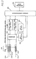
- Shown in Figure 2 is a block diagram of a multichannel data receiver system for capturing data messages generated and transmitted on the ARINC 429 data bus by the subsystems.
- the captured data message in turn may be stored in one of a plurality of memory devices retaining like-kind of information for subsequent use by a data signal processor for obtaining the intended information, for example flight control signals, or navigation position.
- a plurality of data receivers for example remote subsystems are connected to data receivers 210a-c through ARINC 429 data busses 214a-c.
- Data busses 214a-c are serial data busses configured according to the ARINC 429 standard for transmitting the 32 bit data message, including the label word and the subsystem data word, as aforesaid.
- Data receivers 210a-c are intended to temporarily store the data messages, one at a time, in a receiver data register (not shown) until a sequencer 220 issues a receiver reset signal 222a-c.
- Sequencer 220 serves to conditionally receive the receiver data message 224a-c and store the data message in a first capture memory 240 dependent upon whether or not the label word of the received data message matches any of the words stored in a label word look up memory 250. If there is no match between any of the words in the look-up memory 250, sequencer 220 issues a reset signal 222. If there is a match, then the data message is stored in the main memory, and subsequent thereto, the sequencer also issues a reset signal 222, but only after the received data message is stored in the main memory 240.
- first and second secondary memory devices 260 and 270 which are connected to processor interface 280, and a data signal processor 290 which may be a microprocessor or the like.
- Secondary memory devices 260 and 270 which may be a single memory having corresponding first and second memory partitions, are intended to store like-kind data messages, for example all inertial reference data messages, GPS data, or other related information.
- processor 290 served to read the data stored in main memory 240, and transfer the data into one of a plurality of secondary memory devices, for example the two shown in Figure 2.
- Implementation of the system illustrated in Figure 2 generally employ an EPROM (Erasable Programmable Read-Only Memory) for the label look-up memory device.
- EPROM Erasable Programmable Read-Only Memory
- the desired labels are fixedly stored in the EPROM and form part of an electronic hardware package which is onboard the aircraft, and coupled the ARINC 429 busses as illustrated.
- hardware package would need to be modified, and more specifically the EPROM incorporated therein would need to be replaced with one having a new set of desired labels. This procedure is very expensive if the set of desired labels changes frequently.
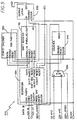
- FIG. 3 Shown in Figure 3 is a block diagram of a multichannel data receiver system in accordance with the present invention for capturing data messages generated and transmitted on a serial data bus and more specifically in accordance with the ARINC 429 data bus system standard. Those blocks in Figure 3 functioning in the same manner as those in Figure 2 have retained the same numeral designation as Figure 1.
- sequencer 320 is operatively connected to receivers 210a-c similar to sequencer 220 shown in Figure 2.
- a random access memory 350 is coupled to microprocessor 390 through processor interface 380 for receiving selected label data information from processor 390 as will be subsequently described.
- first and second memory devices 360 and 370 for selectively storing data messages received by receivers 210a-c as determined by sequencer 320.
- Memory devices 360 and 370 are intended to store data messages of like-kind information in the same manner as that described with respect to secondary memory devices 260 and 270, respectively.
- the label designates what type of information is contained in the information bits. Only selected data messages are needed by other system hardware dependent upon the differing aircraft conditions. In the present invention, only those labels needed by the data signal processor at any given time are written into random access memory 350 by microprocessor 390 as required by the processor for executing specific instructions.
- the label words which are programmed into the random access memory will, of course, change dependent on the differing conditions of the aircraft as aforesaid. For example, the plane will require different data information for when the plane takes off or when the plane is in flight. When the condition changes, microprocessor 390 will erase those label words associated with data messages no longer needed, and write those label words whose data messages are now required. This process is, of course, a very dynamic process.
- the writing and storing of label words into memory 350 may be configured by a variety of techniques to provide efficient interaction with sequencer 320 for determining a) a match with the label word of the received data messages, and b) facilitate storing like-kind data messages in the designated memory, for example GPS or IR, memory devices 360 and 370.
- memory 350 is comprised of two random access memories 350A and 350B, one corresponding to each of the desired like-kind information memory devices.
- Sequencer 320 uses the 8 bit label word plus a 4 bit index word, which designates which receiver is being checked for a match, as an address, a total of 12 bits, for addressing the random access memory 350.
- microprocessor selectively writes a one or 0 in those label word/receiver index address in selected ones of the two random access memories, for example 350A or 350B.
- both memories 350A and 350B are addressed, if a match is found in 350A, the data message is written into memory 360, if a match is found in 350B, the data message is written into memory 370. In some circumstances, the data message may be desired to be written both memories 360 and 370.
- tag bits may be stored in memory 350 address such that the tag word indicates where to store the data messages. It should also be noted that, as indicated in the flow diagram of Figure 4, that any means for directing data messages of like-kind are within the scope of the present invention, and include a check of the label word of the data message itself checked against another look-up table.
- memory devices 260 and 270 are intended to function as a FIFO (first-in, first-out) memory which may be provided by a wide array of components, including an addressable random access memory.
- FIFO first-in, first-out
- FIG. 4 Illustrated in Figure 4 is a flow diagram illustrating the function and operation of sequencer 320 of Figure 3. A description of the sequencer will be described for the special case of 3 receivers 210a-c and two like-kind information memories 360 and 370.
- a pointer or index logic is used to check the status of data ready signal indicative of a stored data message in the receiver data register of each of the receivers, one at a time as indicated by decision block 410.
- the label word is read from the data message stored in the receiver register, block 415.
- the random access memory 350 is interrogated for a determination of a match with a label word stored therein associated with either memory 360 or 370 as indicated by decision blocks 430 and 440 respectively.
- the data is stored, blocks 450 and 455, and subsequently the receiver 210 is reset, block 470 for receiving another data message. If no match was obtained, no data is stored and the receiver is reset. In turn the pointer is incremented to check the next receiver, block 480.
- the data receiver architecture as just described allows for software partitioning and time ordering of received data, particularly ARINC 429 standard data.
- Software partitioning techniques use memory management to apportion access of functions to different memory blocks 360 and 370. Access to these memory blocks by different partitions is strictly controlled by the processor 390. In this way, a failure in one software partition cannot compromise the operation of other partitions. This separation is required in critical avionics functions.
- the time ordering is accomplished in the present invention by the use of FIFO memories 360 and 370, which may be single memory of different partitions.
- GPS Global Positioning Systems
- This data message sorting in accordance with the present invention reduces software overhead since the software kernel is not required to sort and transfer received data messages.
- the like-kind information label words are dynamically alterable by the processor 390.
- the partition separation insures the integrity of the labels in the other partition.
- the dynamic alteration of the label words capability in accordance with present invention allows different label words to be accepted or rejected at varying point in time. For example different points in the flight mission, or data message needed only for initialization, and rejected thereafter.
- the system of the present invention has tremendous advantage over the prior art particularly for GPS/IR system avionic need. This is so since the processor of the prior art had to read unsorted ARINC 429 data and sort and store GPS and IR data in separate memory partitions. The individual software partitions would then read the rewritten data and act upon it. In the present invention, need for sorting and re-writing GPS and IR data while preserving the time ordering of received data is eliminated.
- Receiver 210 is configurable to accept high speed or low speed serial data and convert it to parallel 32 bit words.
- Receiver 210 includes sequencer 504, parity check circuit 510, shift register 520, latch 530, bit counter 540, and multiplexer 550.
- sequencer 504 parity check circuit 510
- shift register 520 shift register 520
- latch 530 latch 530
- bit counter 540 bit counter 540
- multiplexer 550 multiplexer 550.
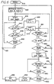
- the operation of the receiver as depicted in Figure 5 is particularly illustrated by the flow diagram of Figure 6, more specifically the function executed by the sequencer circuit 504 of Figure 5.
- Serial ARINC 429 data namely the 32 bit word data in a "three-state" configuration, entered the receiver and is synchronized to the system clock, either high or low speed.
- the receiver resets the bit counter (word gap timer of flow diagram) when a data bit is first received. If 32 bits are received with no word gaps, the word is checked for correct parity by parity check circuit 510. Once a word of proper length is detected, the data word is stored in the output latch 530, and the ready flag signal output is set. If the output latch already has a valid word stored, indicated by the ready flag already being set, the new word is not stored, but discarded. In either case, the receiver is then initialized to get ready to receive another word.
- FIG. 6 thereshown is a flow chart illustrating the flow of data messages in the receiver 2 10 as monitored for correctness by the sequence to obtain high data integrity.
- the data messages are in a "three-state” form so three possible states could exist for each bit of the data message: "1", "0", or no signal.
- a data message from the ARINC 429 enters the receiver 210 and is synchronized to the system clock.
- the shift register 520 is initialized so that all 32 bits are "0”.
- the shift register has 33 bits and the last bit is initialized to "1" so the receiver knows when the data message has completely been transferred.
- the sequencer 504 checks for a "1" or "0" bit.
- the receiver checks for the next data message, because no signal for 4 bit cycles designates the end of a data message. If a "1" or "0" bit is detected, the data message is transferred through the receiver 2 10 to output latch 530. The gap timer or bit counter 540 is reset so that the next gap can be counted to determine if a gap exists in the next data message or if the data message is completely transferred. Once a word gap of the 4 bit cycles is detected, the data is stored in an output latch and the ready flag is set signaling that the data message is available for subsequent processing through sequencer 320 or alternatively 220 of the prior art. If the output latch already has a valid word stored in it, then no new word is stored, but discarded instead. In either case, the receiver is initialized to prepare for receiving more data.
- the receiver rejects wrong frequency data, words with too few bits, words with too many bits, bad parity, and if the previous received word has not been read thereby providing high data integrity.
- the receiver as illustrated herein avoids the need for utilization of the self-clocking characteristics of ARINC 429 standard data. Employment thereof permits the reception of low speed data on high speed channel or reception of word fragments. These conditions allow for processors to perform calculations with corrupted data. Practice of the receiver as disclosed herein provides high data integrity as compared with the self clocking design.
Landscapes
- Engineering & Computer Science (AREA)
- Computer Security & Cryptography (AREA)
- Theoretical Computer Science (AREA)
- Computer Networks & Wireless Communication (AREA)
- Signal Processing (AREA)
- Physics & Mathematics (AREA)
- General Engineering & Computer Science (AREA)
- General Physics & Mathematics (AREA)
- Position Fixing By Use Of Radio Waves (AREA)
- Circuits Of Receivers In General (AREA)
- Mobile Radio Communication Systems (AREA)
Description
- Field of the Invention : The present invention relates to a multi-channel data receiver for an aircraft data bus system. More particularly, the present invention was directed to a multi-channel data system in which the data words are received, examined and directed to designated storage devices.
- The operation of aircraft relies heavily on many electrical subsystems for successful flight missions. These electrical subsystems include, among others, flight management, navigation, auto-pilot, global positioning of systems, landing systems, fuel quantity systems, and the like. Many of these electrical subsystems require communications therebetween, alternatively, sensing subsystems may be located remote from the processing subsystems. Since many of these subsystems may be provided by different manufacturers, standards have been defined for the transfer of data messages on data buses that are wired throughout the aircraft. One such standard is the ARINC (Aeronautical Radio Incorporated) 429 Standard.
- The ARINC 429 Standard is such that each data messages or data word is defined in a number of bits where certain bits define the information which is being communicated, and other bits define a label which indicates how the information bits are to be interpreted. In the ARINC 429, the data message is 32 bit word in which the first 8 bits define the label, and the later 24 bits define the information.
- Multi-channel receiver systems operative with the ARINC 429 Standard, commonly employed a plurality of data receivers for capturing data from a dedicated ARINC 429 data bus. In turn, only selected ones of these data messages having a preselected label were processed to appropriately store the data information into a primary memory. In turn, the information stored in the primary memory was examined for further partitioning into secondary dedicated memory devices, where each of the second memory devices retained like kind information, for example, only GPS data, or only inertial reference data.
- Multi-channel receivers as just described generally store more information in the memory than necessary. This is so, since only certain types of information are required during certain flight operations, for example, in flight, on ground, and take-off. This presents an undue burden on the main memory, and may result in loss of data and poor performance.
- A system according to the introductory part of
claim 1 is shown in EP-A-512 881. - An object of the present invention is to provide a multi-channel data receiver system for efficiently transferring received data into designated memory devices for subsequent usage by one or more system processors. This object is achieved by the apparatus according to the features of
claim 1. - In the present invention, a dynamically active random access memory is utilized for the storage of subsystem label words. In turn a sequencer reads stored data in receivers coupled to a data bus. Depending upon the match of the label word contained in the data message stored in the receiver and those stored in the random access memory, the data message is stored in a like-kind information memory.
-
- Figure 1
- shows examples of different states of an aircraft which require different information from different subsystems.
- Figure 2
- shows a block diagram of a multi-channel ARINC 429 data receiver.
- Figure 3
- is a block diagram of a multi-channel data receiver system in accordance with the present invention.
- Figure 4
- is a flow diagram illustrating the behavior of the multi-channel data receiver system of Figure 3.
- Figure 5
- illustrates a schematic block diagram of the a receiver employed in the block diagram of Figure 3.
- Figure 6
- illustrates a flow diagram illustrating the behavior of the receiver of Figure 5.
- Figure 1 illustrates the employment of a plurality of remote subsystems generating data messages for differing aircraft conditions, for example, in the air, on the ground, and during maintenance. Each of the subsystems generates differing data messages dependent upon differing aircraft conditions. For example,
subsystem 1 generates data messages L1 while in air, and generates data messages L1, L2, and L3 while on the ground. Each of these data messages according the ARINC 429 Standard comprises a 32 bit word where 8 bits are reserved for label information, herein referred to as the label word, and 24 bits are reserved for the subsystem information, herein referred to as the subsystem data word. The label word indicates which subsystem generated the information, and in some circumstances the kind of subsystem information contained in the subsystem data word. - Shown in Figure 2 is a block diagram of a multichannel data receiver system for capturing data messages generated and transmitted on the ARINC 429 data bus by the subsystems. The captured data message in turn may be stored in one of a plurality of memory devices retaining like-kind of information for subsequent use by a data signal processor for obtaining the intended information, for example flight control signals, or navigation position.
- As illustrated in Figure 2, a plurality of data receivers, for example remote subsystems are connected to
data receivers 210a-c through ARINC 429data busses 214a-c.Data busses 214a-c are serial data busses configured according to the ARINC 429 standard for transmitting the 32 bit data message, including the label word and the subsystem data word, as aforesaid. -
Data receivers 210a-c are intended to temporarily store the data messages, one at a time, in a receiver data register (not shown) until asequencer 220 issues a receiver reset signal 222a-c. -
Sequencer 220 serves to conditionally receive thereceiver data message 224a-c and store the data message in afirst capture memory 240 dependent upon whether or not the label word of the received data message matches any of the words stored in a label word look upmemory 250. If there is no match between any of the words in the look-upmemory 250,sequencer 220 issues a reset signal 222. If there is a match, then the data message is stored in the main memory, and subsequent thereto, the sequencer also issues a reset signal 222, but only after the received data message is stored in themain memory 240. - Further illustrated in the prior art configuration of Figure 2, are first and second
secondary memory devices processor interface 280, and adata signal processor 290 which may be a microprocessor or the like.Secondary memory devices processor 290 served to read the data stored inmain memory 240, and transfer the data into one of a plurality of secondary memory devices, for example the two shown in Figure 2. - Implementation of the system illustrated in Figure 2 generally employ an EPROM (Erasable Programmable Read-Only Memory) for the label look-up memory device. The desired labels are fixedly stored in the EPROM and form part of an electronic hardware package which is onboard the aircraft, and coupled the ARINC 429 busses as illustrated. However, in such an implementation, if a different set of label words were desired, hardware package would need to be modified, and more specifically the EPROM incorporated therein would need to be replaced with one having a new set of desired labels. This procedure is very expensive if the set of desired labels changes frequently.
- It should be noted that for the scenario illustrated in Figure 1, all data messages are stored into the main memory even though some messages are unnecessary at different times. Similarly, secondary memory devices are storing unnecessary data messages as well. The sorting system as already described, i.e.
secondary memory devices processor 290 andmain memory 240 may result in loss of data as well as poor performance. This is so, since the sorting system requires much hardware and signal controls to accomplish the intended sorting of the data messages in the secondary memory devices. - Shown in Figure 3 is a block diagram of a multichannel data receiver system in accordance with the present invention for capturing data messages generated and transmitted on a serial data bus and more specifically in accordance with the ARINC 429 data bus system standard. Those blocks in Figure 3 functioning in the same manner as those in Figure 2 have retained the same numeral designation as Figure 1.
- As illustrated in Figure 3,
sequencer 320 is operatively connected toreceivers 210a-c similar tosequencer 220 shown in Figure 2. Arandom access memory 350 is coupled tomicroprocessor 390 throughprocessor interface 380 for receiving selected label data information fromprocessor 390 as will be subsequently described. - Further illustrated in Figure 3 are first and
second memory devices receivers 210a-c as determined bysequencer 320.Memory devices secondary memory devices - As mentioned previously with regard to Figure 1, the label designates what type of information is contained in the information bits. Only selected data messages are needed by other system hardware dependent upon the differing aircraft conditions. In the present invention, only those labels needed by the data signal processor at any given time are written into
random access memory 350 bymicroprocessor 390 as required by the processor for executing specific instructions. The label words which are programmed into the random access memory will, of course, change dependent on the differing conditions of the aircraft as aforesaid. For example, the plane will require different data information for when the plane takes off or when the plane is in flight. When the condition changes,microprocessor 390 will erase those label words associated with data messages no longer needed, and write those label words whose data messages are now required. This process is, of course, a very dynamic process. - The writing and storing of label words into
memory 350 may be configured by a variety of techniques to provide efficient interaction withsequencer 320 for determining a) a match with the label word of the received data messages, and b) facilitate storing like-kind data messages in the designated memory, for example GPS or IR,memory devices memory 350 is comprised of two random access memories 350A and 350B, one corresponding to each of the desired like-kind information memory devices.Sequencer 320 uses the 8 bit label word plus a 4 bit index word, which designates which receiver is being checked for a match, as an address, a total of 12 bits, for addressing therandom access memory 350. Similarly, microprocessor selectively writes a one or 0 in those label word/receiver index address in selected ones of the two random access memories, for example 350A or 350B. - As indicated in the flow diagram, both memories 350A and 350B are addressed, if a match is found in 350A, the data message is written into
memory 360, if a match is found in 350B, the data message is written intomemory 370. In some circumstances, the data message may be desired to be written bothmemories - It should be noted that other schemes are of course possible, having advantages and disadvantages. For example, tag bits may be stored in
memory 350 address such that the tag word indicates where to store the data messages. It should also be noted that, as indicated in the flow diagram of Figure 4, that any means for directing data messages of like-kind are within the scope of the present invention, and include a check of the label word of the data message itself checked against another look-up table. - In the preferred embodiment of the invention,
memory devices - Illustrated in Figure 4 is a flow diagram illustrating the function and operation of
sequencer 320 of Figure 3. A description of the sequencer will be described for the special case of 3receivers 210a-c and two like-kind information memories decision block 410. Upon a data ready signal indicated, the label word is read from the data message stored in the receiver register, block 415. Therandom access memory 350 is interrogated for a determination of a match with a label word stored therein associated with eithermemory receiver 210 is reset, block 470 for receiving another data message. If no match was obtained, no data is stored and the receiver is reset. In turn the pointer is incremented to check the next receiver, block 480. - The data receiver architecture as just described allows for software partitioning and time ordering of received data, particularly
ARINC 429 standard data. Software partitioning techniques use memory management to apportion access of functions todifferent memory blocks processor 390. In this way, a failure in one software partition cannot compromise the operation of other partitions. This separation is required in critical avionics functions. - The time ordering is accomplished in the present invention by the use of
FIFO memories - The like-kind information label words are dynamically alterable by the
processor 390. The partition separation insures the integrity of the labels in the other partition. The dynamic alteration of the label words capability in accordance with present invention allows different label words to be accepted or rejected at varying point in time. For example different points in the flight mission, or data message needed only for initialization, and rejected thereafter. - The system of the present invention has tremendous advantage over the prior art particularly for GPS/IR system avionic need. This is so since the processor of the prior art had to read
unsorted ARINC 429 data and sort and store GPS and IR data in separate memory partitions. The individual software partitions would then read the rewritten data and act upon it. In the present invention, need for sorting and re-writing GPS and IR data while preserving the time ordering of received data is eliminated. - Shown in Figure 5 is schematic block diagram of one embodiment for a
receiver 210.Receiver 210 is configurable to accept high speed or low speed serial data and convert it to parallel 32 bit words.Receiver 210 includessequencer 504,parity check circuit 510, shift register 520,latch 530, bit counter 540, andmultiplexer 550. The operation of the receiver as depicted in Figure 5 is particularly illustrated by the flow diagram of Figure 6, more specifically the function executed by thesequencer circuit 504 of Figure 5. -
Serial ARINC 429 data, namely the 32 bit word data in a "three-state" configuration, entered the receiver and is synchronized to the system clock, either high or low speed. The receiver resets the bit counter (word gap timer of flow diagram) when a data bit is first received. If 32 bits are received with no word gaps, the word is checked for correct parity byparity check circuit 510. Once a word of proper length is detected, the data word is stored in theoutput latch 530, and the ready flag signal output is set. If the output latch already has a valid word stored, indicated by the ready flag already being set, the new word is not stored, but discarded. In either case, the receiver is then initialized to get ready to receive another word. - Referring now to Figure 6, thereshown is a flow chart illustrating the flow of data messages in the
receiver 210 as monitored for correctness by the sequence to obtain high data integrity. The data messages are in a "three-state" form so three possible states could exist for each bit of the data message: "1", "0", or no signal. A data message from theARINC 429 enters thereceiver 210 and is synchronized to the system clock. The shift register 520 is initialized so that all 32 bits are "0". The shift register has 33 bits and the last bit is initialized to "1" so the receiver knows when the data message has completely been transferred. Next, thesequencer 504 checks for a "1" or "0" bit. If no signal exists for 4 bit cycles, the receiver checks for the next data message, because no signal for 4 bit cycles designates the end of a data message. If a "1" or "0" bit is detected, the data message is transferred through thereceiver 210 tooutput latch 530. The gap timer orbit counter 540 is reset so that the next gap can be counted to determine if a gap exists in the next data message or if the data message is completely transferred. Once a word gap of the 4 bit cycles is detected, the data is stored in an output latch and the ready flag is set signaling that the data message is available for subsequent processing throughsequencer 320 or alternatively 220 of the prior art. If the output latch already has a valid word stored in it, then no new word is stored, but discarded instead. In either case, the receiver is initialized to prepare for receiving more data. - In practice of the receiver as illustrated by Figures 5 and 6, the receiver rejects wrong frequency data, words with too few bits, words with too many bits, bad parity, and if the previous received word has not been read thereby providing high data integrity.
- The receiver as illustrated herein avoids the need for utilization of the self-clocking characteristics of
ARINC 429 standard data. Employment thereof permits the reception of low speed data on high speed channel or reception of word fragments. These conditions allow for processors to perform calculations with corrupted data. Practice of the receiver as disclosed herein provides high data integrity as compared with the self clocking design. - Although a specific embodiment has been shown for multichannel data receiver system in accordance with present invention, others are of course possible within the level of skill in the art, and are within the scope of the present invention.
- More specifically, the foregoing description has been set forth in terms of functional block diagrams including registers, counters, timers, and logic means, and also illustrated in terms of flow diagrams to enhance understanding of the present invention without burdening the reader with detail well known within the level of those skilled in the art. There are, of course, a wide array of implementations for achieving the intended function as depicted in the accompanying claim, all of which are intended to be within the scope of the present invention. It should also be noted that although a specific embodiment has been illustrating specific memory devices, there are of course a wide array of components for serving the intended function. More specifically, FIFO memories may be implemented by an addressable random access memory. Lastly, although the embodiment of the invention has been illustrated, at least in part, by specific data transfer being serial or parallel, alternate arrangements are, of course, within the scope of the present invention as defined by the accompanying claim.
- It should also be noted that all, or selected ones of any of the electrical circuit components may be configured into a single integrated circuit and that the separation of components as illustrated in the Figures is within the scope of the present invention as defined by the accompanying claim.
Claims (1)
- A multichannel data receiver system for distributing data messages received on a data bus to a plurality of like-kind information memory devices, where said like-kind information are messages having a label word which belongs to a predefined set of label words, and where said data messages have a fixed word bit length in which a plurality of bits define a label word indicating the subsystem origin of said data message, and the remainder bits define an information data word,
comprising:characterized by:receivers (210a - 210c) coupled to a serial data bus for receiving said data messages and providing a data ready signal indicative that said data message is stored in a data register therein;a random access memory means (350) for storing label words;a data signal processor (390) coupled to said random access memory for selectively erasing label words stored in said random access memory and storing selected label words in said random access memory;at least first and second secondary memory devices (360, 370) for storing data messages of like-kind information, whereby at least two different sets of label words are stored in at least two different memory sectors; anda sequencer means (320) which compares the label word stored in said receiver data register to label words stored in all sections of said random access memory means, and if the label words from said receiver and a section of said random access memory means match, the sequencer means (320) stores the data messages to the secondary memory device corresponding to that section of the random access memory means.
Applications Claiming Priority (2)
| Application Number | Priority Date | Filing Date | Title |
|---|---|---|---|
| US08/099,794 US5424949A (en) | 1993-07-30 | 1993-07-30 | Multi-channel data receiver system |
| US99794 | 1993-07-30 |
Publications (2)
| Publication Number | Publication Date |
|---|---|
| EP0636989A1 EP0636989A1 (en) | 1995-02-01 |
| EP0636989B1 true EP0636989B1 (en) | 1999-05-19 |
Family
ID=22276656
Family Applications (1)
| Application Number | Title | Priority Date | Filing Date |
|---|---|---|---|
| EP94111603A Expired - Lifetime EP0636989B1 (en) | 1993-07-30 | 1994-07-26 | Multi-channel data receiver system |
Country Status (4)
| Country | Link |
|---|---|
| US (1) | US5424949A (en) |
| EP (1) | EP0636989B1 (en) |
| CA (1) | CA2129065A1 (en) |
| DE (1) | DE69418545T2 (en) |
Families Citing this family (10)
| Publication number | Priority date | Publication date | Assignee | Title |
|---|---|---|---|---|
| JPH05205005A (en) * | 1990-03-30 | 1993-08-13 | Internatl Business Mach Corp <Ibm> | Host-interface for logic-simulation-machine |
| FR2743966B1 (en) * | 1996-01-19 | 1998-02-20 | Sextant Avionique | METHOD FOR TIME MANAGEMENT OF A MULTIPLEX BUS |
| US6671589B2 (en) * | 2001-02-13 | 2003-12-30 | William Holst | Method and apparatus to support remote and automatically initiated data loading and data acquisition of airborne computers using a wireless spread spectrum aircraft data services link |
| US7908042B2 (en) * | 2001-02-13 | 2011-03-15 | The Boeing Company | Methods and apparatus for wireless upload and download of aircraft data |
| KR20070012308A (en) | 2003-09-02 | 2007-01-25 | 서프 테크놀러지, 인코포레이티드 | Signal Processing System for Satellite Position Signals |
| US7256749B2 (en) * | 2005-05-17 | 2007-08-14 | The Boeing Company | Compact, mechanically scanned cassegrain antenna system and method |
| US7180437B1 (en) * | 2005-08-03 | 2007-02-20 | The Boeing Company | Parallel-to-serial converter |
| US8292543B2 (en) * | 2008-04-28 | 2012-10-23 | Waste Management, Inc. | Multi-planar gas recovery bioreactor |
| US8335609B2 (en) * | 2010-01-25 | 2012-12-18 | United Technologies Corporation | Method and system for exposing and recording embedded avionics data |
| US9485113B2 (en) | 2013-10-11 | 2016-11-01 | Ge Aviation Systems Llc | Data communications network for an aircraft |
Family Cites Families (13)
| Publication number | Priority date | Publication date | Assignee | Title |
|---|---|---|---|---|
| US4486853A (en) * | 1981-04-01 | 1984-12-04 | Telemet American, Inc. | Apparatus for receiving and displaying continuously updated data |
| US4499576A (en) * | 1982-08-13 | 1985-02-12 | At&T Bell Laboratories | Multiplexed first-in, first-out queues |
| US4755929A (en) * | 1984-09-28 | 1988-07-05 | The Boeing Company | Apparatus and method for retrieving data in the form of binary, multiple bit, digital communication words from a system bus |
| US4729102A (en) * | 1984-10-24 | 1988-03-01 | Sundstrand Data Control, Inc. | Aircraft data acquisition and recording system |
| US4809217A (en) * | 1985-10-31 | 1989-02-28 | Allen-Bradley Company, Inc. | Remote I/O port for transfer of I/O data in a programmable controller |
| US5167020A (en) * | 1989-05-25 | 1992-11-24 | The Boeing Company | Serial data transmitter with dual buffers operating separately and having scan and self test modes |
| US5019980A (en) * | 1989-07-14 | 1991-05-28 | The Boeing Company | General purpose avionics display monitor |
| US5321816A (en) * | 1989-10-10 | 1994-06-14 | Unisys Corporation | Local-remote apparatus with specialized image storage modules |
| US5133081A (en) * | 1989-11-03 | 1992-07-21 | Mayo Scott T | Remotely controllable message broadcast system including central programming station, remote message transmitters and repeaters |
| US5218680A (en) * | 1990-03-15 | 1993-06-08 | International Business Machines Corporation | Data link controller with autonomous in tandem pipeline circuit elements relative to network channels for transferring multitasking data in cyclically recurrent time slots |
| FR2676319B1 (en) * | 1991-05-07 | 1993-12-10 | Sextant Avionique | METHOD AND DEVICE FOR SELECTING INFORMATION FOR USE BY A LOCAL UNIT CONNECTED TO A DIGITAL TRANSMISSION SYSTEM. |
| US5349685A (en) * | 1992-05-05 | 1994-09-20 | The United States Of America As Represented By The Secretary Of The Navy | Multipurpose bus interface utilizing a digital signal processor |
| US5307505A (en) * | 1992-05-05 | 1994-04-26 | The United States Of America As Represented By The Secretary Of The Navy | Rapid reprogramming terminal |
-
1993
- 1993-07-30 US US08/099,794 patent/US5424949A/en not_active Expired - Lifetime
-
1994
- 1994-07-26 DE DE69418545T patent/DE69418545T2/en not_active Expired - Fee Related
- 1994-07-26 EP EP94111603A patent/EP0636989B1/en not_active Expired - Lifetime
- 1994-07-28 CA CA002129065A patent/CA2129065A1/en not_active Abandoned
Also Published As
| Publication number | Publication date |
|---|---|
| DE69418545D1 (en) | 1999-06-24 |
| DE69418545T2 (en) | 1999-12-23 |
| US5424949A (en) | 1995-06-13 |
| EP0636989A1 (en) | 1995-02-01 |
| CA2129065A1 (en) | 1995-01-31 |
Similar Documents
| Publication | Publication Date | Title |
|---|---|---|
| EP0185609B1 (en) | Coherent interface with wraparound receive and transmit memories | |
| KR0161101B1 (en) | Network adapter with host interrupt and indication management | |
| EP0184976B1 (en) | Apparatus for interfacing between at least one channel and at least one bus | |
| CA2119152C (en) | Network interface with host independent buffer management | |
| EP0211500B1 (en) | Data control system for digital automatic flight control system channel with plural dissimilar data processing | |
| EP0118446B1 (en) | First-in, first-out (fifo) memory configuration for queue storage | |
| US4494190A (en) | FIFO buffer to cache memory | |
| US5890007A (en) | Multi-cluster parallel processing computer system | |
| US5093780A (en) | Inter-processor transmission system having data link which automatically and periodically reads and writes the transfer data | |
| EP0859311A1 (en) | First in, first out (FIFO) data buffering system | |
| EP0464433A2 (en) | Microcontroller device having remotely programmable EPROM & method of programming | |
| US5424949A (en) | Multi-channel data receiver system | |
| US5594927A (en) | Apparatus and method for aligning data transferred via DMA using a barrel shifter and a buffer comprising of byte-wide, individually addressabe FIFO circuits | |
| EP0188990B1 (en) | Coherent interface with wraparound receive memory | |
| US7093070B2 (en) | Method and system for selectively recording system information | |
| US20180349300A1 (en) | Hardware queue manager with water marking | |
| US4638430A (en) | EAROM and EEPROM data storage management | |
| EP0072927B1 (en) | Device for addressing a memory | |
| US3535696A (en) | Data compression system with a minimum time delay unit | |
| CA2129157C (en) | Arinc 629 data receiver system | |
| US5343557A (en) | Workstation controller with full screen write mode and partial screen write mode | |
| GB2111271A (en) | Data transmission and processing systems | |
| US20020040414A1 (en) | Multiprocessor system and transaction control method for the same | |
| KR20010053612A (en) | Storage device and a method for operating the storage device | |
| US5012404A (en) | Integrated circuit remote terminal stores interface for communication between CPU and serial bus |
Legal Events
| Date | Code | Title | Description |
|---|---|---|---|
| PUAI | Public reference made under article 153(3) epc to a published international application that has entered the european phase |
Free format text: ORIGINAL CODE: 0009012 |
|
| AK | Designated contracting states |
Kind code of ref document: A1 Designated state(s): DE FR GB IT |
|
| 17P | Request for examination filed |
Effective date: 19950203 |
|
| 17Q | First examination report despatched |
Effective date: 19980428 |
|
| GRAG | Despatch of communication of intention to grant |
Free format text: ORIGINAL CODE: EPIDOS AGRA |
|
| GRAG | Despatch of communication of intention to grant |
Free format text: ORIGINAL CODE: EPIDOS AGRA |
|
| GRAH | Despatch of communication of intention to grant a patent |
Free format text: ORIGINAL CODE: EPIDOS IGRA |
|
| GRAH | Despatch of communication of intention to grant a patent |
Free format text: ORIGINAL CODE: EPIDOS IGRA |
|
| GRAA | (expected) grant |
Free format text: ORIGINAL CODE: 0009210 |
|
| AK | Designated contracting states |
Kind code of ref document: B1 Designated state(s): DE FR GB IT |
|
| REF | Corresponds to: |
Ref document number: 69418545 Country of ref document: DE Date of ref document: 19990624 |
|
| ET | Fr: translation filed | ||
| PLBE | No opposition filed within time limit |
Free format text: ORIGINAL CODE: 0009261 |
|
| STAA | Information on the status of an ep patent application or granted ep patent |
Free format text: STATUS: NO OPPOSITION FILED WITHIN TIME LIMIT |
|
| 26N | No opposition filed | ||
| REG | Reference to a national code |
Ref country code: GB Ref legal event code: IF02 |
|
| PGFP | Annual fee paid to national office [announced via postgrant information from national office to epo] |
Ref country code: GB Payment date: 20050614 Year of fee payment: 12 |
|
| PGFP | Annual fee paid to national office [announced via postgrant information from national office to epo] |
Ref country code: FR Payment date: 20050706 Year of fee payment: 12 |
|
| PGFP | Annual fee paid to national office [announced via postgrant information from national office to epo] |
Ref country code: DE Payment date: 20050729 Year of fee payment: 12 |
|
| PG25 | Lapsed in a contracting state [announced via postgrant information from national office to epo] |
Ref country code: GB Free format text: LAPSE BECAUSE OF NON-PAYMENT OF DUE FEES Effective date: 20060726 |
|
| PGFP | Annual fee paid to national office [announced via postgrant information from national office to epo] |
Ref country code: IT Payment date: 20060731 Year of fee payment: 13 |
|
| PG25 | Lapsed in a contracting state [announced via postgrant information from national office to epo] |
Ref country code: DE Free format text: LAPSE BECAUSE OF NON-PAYMENT OF DUE FEES Effective date: 20070201 |
|
| GBPC | Gb: european patent ceased through non-payment of renewal fee |
Effective date: 20060726 |
|
| REG | Reference to a national code |
Ref country code: FR Ref legal event code: ST Effective date: 20070330 |
|
| PG25 | Lapsed in a contracting state [announced via postgrant information from national office to epo] |
Ref country code: FR Free format text: LAPSE BECAUSE OF NON-PAYMENT OF DUE FEES Effective date: 20060731 |
|
| PG25 | Lapsed in a contracting state [announced via postgrant information from national office to epo] |
Ref country code: IT Free format text: LAPSE BECAUSE OF NON-PAYMENT OF DUE FEES Effective date: 20070726 |
|
| P01 | Opt-out of the competence of the unified patent court (upc) registered |
Effective date: 20230525 |