EP0629022A1 - Cell with terminals and circuit substrate - Google Patents
Cell with terminals and circuit substrate Download PDFInfo
- Publication number
- EP0629022A1 EP0629022A1 EP94303843A EP94303843A EP0629022A1 EP 0629022 A1 EP0629022 A1 EP 0629022A1 EP 94303843 A EP94303843 A EP 94303843A EP 94303843 A EP94303843 A EP 94303843A EP 0629022 A1 EP0629022 A1 EP 0629022A1
- Authority
- EP
- European Patent Office
- Prior art keywords
- cell
- terminals
- circuit substrate
- terminal
- pair
- Prior art date
- Legal status (The legal status is an assumption and is not a legal conclusion. Google has not performed a legal analysis and makes no representation as to the accuracy of the status listed.)
- Granted
Links
Images


Classifications
-
- H—ELECTRICITY
- H01—ELECTRIC ELEMENTS
- H01M—PROCESSES OR MEANS, e.g. BATTERIES, FOR THE DIRECT CONVERSION OF CHEMICAL ENERGY INTO ELECTRICAL ENERGY
- H01M50/00—Constructional details or processes of manufacture of the non-active parts of electrochemical cells other than fuel cells, e.g. hybrid cells
- H01M50/50—Current conducting connections for cells or batteries
- H01M50/528—Fixed electrical connections, i.e. not intended for disconnection
-
- H—ELECTRICITY
- H01—ELECTRIC ELEMENTS
- H01R—ELECTRICALLY-CONDUCTIVE CONNECTIONS; STRUCTURAL ASSOCIATIONS OF A PLURALITY OF MUTUALLY-INSULATED ELECTRICAL CONNECTING ELEMENTS; COUPLING DEVICES; CURRENT COLLECTORS
- H01R12/00—Structural associations of a plurality of mutually-insulated electrical connecting elements, specially adapted for printed circuits, e.g. printed circuit boards [PCB], flat or ribbon cables, or like generally planar structures, e.g. terminal strips, terminal blocks; Coupling devices specially adapted for printed circuits, flat or ribbon cables, or like generally planar structures; Terminals specially adapted for contact with, or insertion into, printed circuits, flat or ribbon cables, or like generally planar structures
- H01R12/50—Fixed connections
- H01R12/51—Fixed connections for rigid printed circuits or like structures
- H01R12/55—Fixed connections for rigid printed circuits or like structures characterised by the terminals
- H01R12/58—Fixed connections for rigid printed circuits or like structures characterised by the terminals terminals for insertion into holes
-
- H—ELECTRICITY
- H01—ELECTRIC ELEMENTS
- H01M—PROCESSES OR MEANS, e.g. BATTERIES, FOR THE DIRECT CONVERSION OF CHEMICAL ENERGY INTO ELECTRICAL ENERGY
- H01M50/00—Constructional details or processes of manufacture of the non-active parts of electrochemical cells other than fuel cells, e.g. hybrid cells
- H01M50/20—Mountings; Secondary casings or frames; Racks, modules or packs; Suspension devices; Shock absorbers; Transport or carrying devices; Holders
- H01M50/204—Racks, modules or packs for multiple batteries or multiple cells
- H01M50/207—Racks, modules or packs for multiple batteries or multiple cells characterised by their shape
- H01M50/216—Racks, modules or packs for multiple batteries or multiple cells characterised by their shape adapted for button or coin cells
-
- H—ELECTRICITY
- H01—ELECTRIC ELEMENTS
- H01M—PROCESSES OR MEANS, e.g. BATTERIES, FOR THE DIRECT CONVERSION OF CHEMICAL ENERGY INTO ELECTRICAL ENERGY
- H01M50/00—Constructional details or processes of manufacture of the non-active parts of electrochemical cells other than fuel cells, e.g. hybrid cells
- H01M50/50—Current conducting connections for cells or batteries
- H01M50/543—Terminals
- H01M50/547—Terminals characterised by the disposition of the terminals on the cells
- H01M50/548—Terminals characterised by the disposition of the terminals on the cells on opposite sides of the cell
-
- H—ELECTRICITY
- H01—ELECTRIC ELEMENTS
- H01M—PROCESSES OR MEANS, e.g. BATTERIES, FOR THE DIRECT CONVERSION OF CHEMICAL ENERGY INTO ELECTRICAL ENERGY
- H01M50/00—Constructional details or processes of manufacture of the non-active parts of electrochemical cells other than fuel cells, e.g. hybrid cells
- H01M50/50—Current conducting connections for cells or batteries
- H01M50/543—Terminals
- H01M50/552—Terminals characterised by their shape
- H01M50/559—Terminals adapted for cells having curved cross-section, e.g. round, elliptic or button cells
-
- H—ELECTRICITY
- H01—ELECTRIC ELEMENTS
- H01M—PROCESSES OR MEANS, e.g. BATTERIES, FOR THE DIRECT CONVERSION OF CHEMICAL ENERGY INTO ELECTRICAL ENERGY
- H01M50/00—Constructional details or processes of manufacture of the non-active parts of electrochemical cells other than fuel cells, e.g. hybrid cells
- H01M50/50—Current conducting connections for cells or batteries
- H01M50/543—Terminals
- H01M50/562—Terminals characterised by the material
-
- H—ELECTRICITY
- H01—ELECTRIC ELEMENTS
- H01R—ELECTRICALLY-CONDUCTIVE CONNECTIONS; STRUCTURAL ASSOCIATIONS OF A PLURALITY OF MUTUALLY-INSULATED ELECTRICAL CONNECTING ELEMENTS; COUPLING DEVICES; CURRENT COLLECTORS
- H01R13/00—Details of coupling devices of the kinds covered by groups H01R12/70 or H01R24/00 - H01R33/00
- H01R13/02—Contact members
- H01R13/10—Sockets for co-operation with pins or blades
- H01R13/11—Resilient sockets
- H01R13/115—U-shaped sockets having inwardly bent legs, e.g. spade type
-
- H—ELECTRICITY
- H01—ELECTRIC ELEMENTS
- H01M—PROCESSES OR MEANS, e.g. BATTERIES, FOR THE DIRECT CONVERSION OF CHEMICAL ENERGY INTO ELECTRICAL ENERGY
- H01M2220/00—Batteries for particular applications
- H01M2220/30—Batteries in portable systems, e.g. mobile phone, laptop
-
- Y—GENERAL TAGGING OF NEW TECHNOLOGICAL DEVELOPMENTS; GENERAL TAGGING OF CROSS-SECTIONAL TECHNOLOGIES SPANNING OVER SEVERAL SECTIONS OF THE IPC; TECHNICAL SUBJECTS COVERED BY FORMER USPC CROSS-REFERENCE ART COLLECTIONS [XRACs] AND DIGESTS
- Y02—TECHNOLOGIES OR APPLICATIONS FOR MITIGATION OR ADAPTATION AGAINST CLIMATE CHANGE
- Y02E—REDUCTION OF GREENHOUSE GAS [GHG] EMISSIONS, RELATED TO ENERGY GENERATION, TRANSMISSION OR DISTRIBUTION
- Y02E60/00—Enabling technologies; Technologies with a potential or indirect contribution to GHG emissions mitigation
- Y02E60/10—Energy storage using batteries
Definitions
- the present invention relates to a cell with terminals on which the cell can detachably be mounted, and to a circuit substrate.
- a primary or a secondary cell such as lithium, alkali and the like in the form of a coin, a button and a cylinder is frequently used as a backup power source for backing up various memories such as an electronic instrument or the like.
- the present invention intends to solve the above-discussed problems, and an object of the invention is to provide a cell with terminals in which an exchange of the cell is easy and in which a fixing strength of the cell is excellent, and a circuit substrate.
- a structure which is provided with a pair of engaging portions which are formed by forward end surfaces in which peripheral ends are processed in bending into arcuation so as to form a pair of openings in one surface, and forward end surfaces of respective projections, preferably, spherical segments which partially project inwardly in the other surface, and a structure is selected in which a pair of elements to be mounted are urged and fixed by stable firm elasticity or resiliency of the inwardly projecting projections, preferably, of the spherical segments in the engaging portions, respectively.
- the terminal elements, the mounting elements and the terminal elements to be mounted material is selected in which a wall thickness is within a range of 0.15 mm - 1.0 mm, a Vickers hardness is equal to or less than 250 HV conventionally as use material of this kind, and a spring limit or critical value is less than 30 kgf/mm2.
- the cell with terminals or the circuit substrate according to the present invention is arranged such that the Vickers hardness is 250 - 450 HV, and the spring critical value is 30 - 60 kgf/mm2, and is made of stainless material, nickel material, composite material thereof or the like, in which a distance of the engaging spaces in each of the engaging portions is shorter 0.1 - 0.5 mm than the wall thickness of the element to be mounted.
- the cell with terminals on which the terminal elements according to the present invention are mounted or the circuit substrate it is possible to detachably perform exchange of the cell, and a firm crimp condition due to a spring pressure which is generated in view of structure can always be maintained.
- the cell with terminals and the circuit substrate are extremely advantageous in economic such as handling, recycling or the like.
- FIGs. 1 to 5 an embodiment of the present invention is shown in Figs. 1 to 5.
- the description will be made as an example of a cell with terminals, which is provided with a pair of terminal elements according to the present invention respectively on surfaces of respective terminals of the cell which is shown as the embodiment.
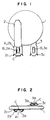
- Fig. 1 is a front elevational view showing a condition under which terminal elements 2 and 3 according to the present invention are welded and fixed respectively to terminal surfaces of respective positive and negative poles of a coin-shaped lithium cell 1, by means of laser welding.
- the terminal elements 2 and 3 have respective forward ends thereof which define engaging-portion spaces C , respectively, in mating terminals, which are defined respectively by portions 2b and 3b processed in bending into the form of an arcuation so as to form openings in one surfaces A , respectively, as shown in an enlarged cross-sectional view of a principal portion in Fig. 5, and projections 2a and 3a partially projecting inwardly in the other surfaces B , respectively.
- the reference characters 2c and 3c denote terminal inserting guides upon mounting of the terminals of the mating equipment, or positioning guides.
- Fig. 2 is a top plan view of Fig. 1, while Fig. 3 is a side elevational view of Fig. 1.
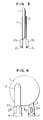
- Fig. 4 is a front elevational view showing a condition at the time a pair of mating plain-plate like terminal elements 4 are fitted respectively in the engaging-portion spaces C .
- Fig. 5 is a cross-sectional view taken along a line V - V in Fig. 4. Accordingly, Fig. 5 shows a cross-section of a condition under which the plain-plate like terminal elements 4 which are provided on the mating equipment are fitted.
- the terminal elements 4 are engaged with and fixedly mounted on, respectively, the terminal elements according to the present invention, that is, are engaged with and fixedly mounted on, under the crimp condition, respectively the engaging-portion spaces C which are defined by forward-end partial surfaces A2 and A3 of the respective portions 2b and 3b in which peripheral ends are worked in bending into an arcuate form with the same radius of curvature so as to form an opening A1 in one surface A , and a forward-end surface B1 of the projections 2a and 3a which partially project inwardly in the other surface B .
- the arrangement is such that, when it is assumed that a spacing between the forward-end partial surfaces A2 and A3 and the forward-end surface B1 of the projection is D , and that the wall thickness of each of the mating terminal elements 4 is T , then, D and T satisfy the following relationship indicated by the equation (2).
- T - D ⁇ 0.1 - 0.5
- the terminal elements according to the present invention are formed by metallic material whose wall thickness is 0.15 - 1.0 mm, whose Vickers hardness is 250 - 450 HV, and whose spring elastic modulus is 30 - 60 kgf/mm2. The reason why the wall thickness is 0.15 - 1.0 mm is as follows.
- the wall thickness is equal to or less than 0.15 mm
- the spring elastic modulus is 30 - 60 kgf/mm2
- the Vickers hardness is 250 - 450 HV as the fixed mounting strength of the terminal elements
- the reason why the Vickers hardness is 250 - 450 HV and the spring elastic modulus is 30 - 60 kgf/mm2 is that material in which the Vickers hardness is less than 250 HV and the spring limit value is less than 30 kgf/mm2 has conventionally been used as terminal material of this kind.
- the material on this order is weak or low in strength as an arrangement and the use of the invention, and is not used for the following reason. That is, in a case of material in which the spring limit value is 30 kgf/mm2, repeating of mounting and demounting of the cell causes the spring restoring force to be embrittled.
- the terminals are deformed.
- the Vickers hardness is equal to or more than 450 HV
- the hardness of the material is too high upon application of oscillation, there are many cases where the terminal elements are broken by stress concentration.
- radius of curvature is of the order of twice the wall thickness.
- processing cannot be performed if the radius of curvature is of the order of five times the wall thickness. This is not preferable in view of space-saving.
- the material of the terminal elements and the material of the terminals to be mounted of this kind material is required in which the material of the terminal elements and the material of the terminals to be mounted are substantially the same in wall thickness as each other, the wall thickness is within a range of from 0.15 mm - 1.0 mm, the Vickers hardness is 250 - 450 HV, and the spring elastic modulus is within a range of from 30 - 60 kgf/mm2.
- Figs. 6 to 10 show an embodiment which is provided with another pair of terminal elements according to the present invention.
- the arrangement of the embodiment is similar to that of the embodiment illustrated in Figs. 1 to 5 except that the projections 2a and 3a which project inwardly in the other surfaces B of the respective forward ends of the terminal elements 2 and 3 are spherical segments 2a' and 3a'. Further, B1' denotes a forward end surface of the spherical segment.
- FIG. 1 shows experimental results which find out the relationship between an engaging-portion spatial distance D according to the present invention and the wall thickness T of the material to be mounted that is a plain-plate like terminal element.
- TABLE 2 shows the results in a case where nickel material whose wall thickness is 0.5 mm, whose Vickers hardness is 300 HV, and whose spring elastic modulus is 32 kgf/mm2 is used.
- TABLE 3 shows the comparison between terminal element material in which wall thickness of each of the terminal elements to be mounted is 0.3 mm and has a material value according to the present invention, specifically, material whose Vickers hardness is 300 HV, whose spring elastic modulus is 40 kgf/mm2 and material having the conventional material value, specifically, a case where material whose Vickers hardness is 230 HV and whose spring elastic modulus is 25 kgf/mm2 is used as terminal element material.
- either of the terminal element materials use stainless steel material, and the experiment was carried into practice by a radius of curvature of bent working portion in the form of an arcuation of the terminals is processed to R twice the wall thickness.
- the present embodiment illustrated in (TABLE 3) shows an example in which stainless steel material whose wall thickness is 0.3 mm is used.
- material other than the stainless steel is individual of nickel material, copper material, steel material, phosphor bronze, brass, aluminum copper or the like having physical properties within a range according to the present invention, or composite material such as clad material, or surface-treatment working or processing material, there are provided advantages similar to those of the experiment results shown in (TABLE 1), (TABLE 2) and (TABLE 3), and the former materials can be used.
- Fig. 11 shows another embodiment of the present invention, and is a side elevational diagrammatic view showing an example in which a pair of terminal mounting elements 6 according to the present invention are provided on the circuit substrate 5. That is, Fig. 6 shows a condition at the time a cell in which a pair of plain-plate like terminals 7 are mounted respectively on positive and negative pole terminal surfaces of a cell 1 is inserted into a pair of terminal mounting elements which are provided on a circuit substrate. Similar experiments show that there can be produced advantages similar to the aforesaid advantages, by the fact that the arrangement of the terminal mounting elements is brought to the arrangement of the present invention.
- the invention ensures retention of the cell in the form of a coin, a button, a cylinder, a square shape or the like, by the fact that the mating terminals are clamped respectively to the engaging spaces formed respectively by the portions in which the peripheral ends are processed or worked in bending into the arcuate form so as to form the openings in the one surfaces, and the projections, preferably, the spherical segments which partially project inwardly on the other surfaces, and are crimped and fixed respectively to the engaging spaces, whereby such a force as to be clamped by the firm spring pressure always acts upon the mating terminals.
- the present invention is high in oscillation proof, can maintain the electric contact condition with respect to the mating terminals excellent in a long period of time, and extremely facilitates disconnection or dismounting and equipment of the cell, because the portions abutted when the mating terminals are inserted form the projections, preferably, the spherical segments.
Landscapes
- Chemical & Material Sciences (AREA)
- Chemical Kinetics & Catalysis (AREA)
- Electrochemistry (AREA)
- General Chemical & Material Sciences (AREA)
- Connection Of Batteries Or Terminals (AREA)
- Battery Mounting, Suspending (AREA)
Abstract
Description
- The present invention relates to a cell with terminals on which the cell can detachably be mounted, and to a circuit substrate.
- Generally, a primary or a secondary cell such as lithium, alkali and the like in the form of a coin, a button and a cylinder is frequently used as a backup power source for backing up various memories such as an electronic instrument or the like. An arrangement in which terminals are mounted on the cell of this kind by a method of resistance welding, laser welding (YAG laser, exima laser or CO₂ laser) or the like is directly mounted on a circuit substrate by soldering. In this case, operation for exchanging the cell at the time the service life of the cell is reduced or at the time the guaranteed period of time of the cell service life is reached is troublesome. Further, when a recent recycle utilization of resources is considered, the necessity of recycle has been desired for a cell which uses various kinds of metallic oxides and rare metals such as lithium, zinc and the like. For this reason, as disclosed in Japanese Patent Unexamined Publication No. 60-131753 and Japanese Patent Publication No. 3-40464, a cell holder has been used in which a cell can easily be retrieved.
- In a case where the cell is mounted on the cell holder and is used, a space for receiving the cell holder into a circuit substrate is required. Particularly, when it is considered that recent miniaturization or small-sizing of electronic equipments is used widely, it is difficult to provide a space for receiving the cell holder within the circuit substrate.
- The present invention intends to solve the above-discussed problems, and an object of the invention is to provide a cell with terminals in which an exchange of the cell is easy and in which a fixing strength of the cell is excellent, and a circuit substrate.
- In order to solve these problems, in the present invention, consideration is applied to a structure and material of a pair of mounting elements of a pair of plain-plate like terminals which are mounted respectively on terminal elements mounted respectively on surfaces of terminals of a cell which are mounted on a pair of plain-plate like terminals of a mating instrument, or which are mounted respectively on surfaces of respective cell terminals which are provided on a circuit substrate. Specifically, as a structure of the terminal elements which are mounted respectively on the terminal surfaces of the cell, or as a structure of the mounting elements of the plain-plate like cell terminals which are provided on the circuit substrate, a structure is selected which is provided with a pair of engaging portions which are formed by forward end surfaces in which peripheral ends are processed in bending into arcuation so as to form a pair of openings in one surface, and forward end surfaces of respective projections, preferably, spherical segments which partially project inwardly in the other surface, and a structure is selected in which a pair of elements to be mounted are urged and fixed by stable firm elasticity or resiliency of the inwardly projecting projections, preferably, of the spherical segments in the engaging portions, respectively. Thus, the above-discussed problems are solved.
- Moreover, as material of the terminal elements, the mounting elements and the terminal elements to be mounted, material is selected in which a wall thickness is within a range of 0.15 mm - 1.0 mm, a Vickers hardness is equal to or less than 250 HV conventionally as use material of this kind, and a spring limit or critical value is less than 30 kgf/mm². However, the cell with terminals or the circuit substrate according to the present invention is arranged such that the Vickers hardness is 250 - 450 HV, and the spring critical value is 30 - 60 kgf/mm², and is made of stainless material, nickel material, composite material thereof or the like, in which a distance of the engaging spaces in each of the engaging portions is shorter 0.1 - 0.5 mm than the wall thickness of the element to be mounted.
- By the use of the cell with terminals on which the terminal elements according to the present invention are mounted or the circuit substrate, it is possible to detachably perform exchange of the cell, and a firm crimp condition due to a spring pressure which is generated in view of structure can always be maintained. Thus, the cell with terminals and the circuit substrate are extremely advantageous in economic such as handling, recycling or the like.
-
- Fig. 1 is a front elevational view showing a coin-shaped cell which is provided with a pair of terminal elements according to the present invention;
- Fig. 2 is a top plan view showing the coin-shaped cell which is provided with the pair of terminal elements according to the present invention;
- Fig. 3 is a side elevational view showing the coin-shaped cell which is provided with the pair of terminal elements according to the present invention;
- Fig. 4 is a front elevational view of a condition under which a pair of plain-plate like terminal elements of a mating equipment are fitted respectively in the terminal elements according to the present invention;
- Fig. 5 is a cross-sectional view of a principal portion under a condition in which the plain-plate like terminal elements of the mating equipment are fitted respectively in the terminal elements according to the present invention;
- Fig. 6 is a front elevational view showing a coin-shaped cell which is provided with other terminal elements according to the present invention;
- Fig. 7 is a front elevational view showing the coin-shaped cell which is provided with the other terminal elements according to the present invention;
- Fig. 8 is a side elevational view showing the coin-shaped cell which is provided with the other terminal elements according to the present invention;
- Fig. 9 is a front elevational view of a condition in which a pair of plain-plate like terminal elements of a mating equipment are fitted respectively in a pair of other terminal elements according to the present invention;
- Fig. 10 is a cross-sectional view of a principal portion under a condition in which the plain-plate like terminal elements of the mating equipment are fitted respectively in the other terminal elements according to the present invention; and
- Fig. 11 is a side elevational diagrammatic view showing the other embodiment of the present invention.
- Hereunder, an embodiment of the present invention is shown in Figs. 1 to 5. In this connection, the description will be made as an example of a cell with terminals, which is provided with a pair of terminal elements according to the present invention respectively on surfaces of respective terminals of the cell which is shown as the embodiment.
- Fig. 1 is a front elevational view showing a condition under which
terminal elements terminal elements portions projections reference characters - Fig. 2 is a top plan view of Fig. 1, while Fig. 3 is a side elevational view of Fig. 1.
- Fig. 4 is a front elevational view showing a condition at the time a pair of mating plain-plate like
terminal elements 4 are fitted respectively in the engaging-portion spaces C. Fig. 5 is a cross-sectional view taken along a line V - V in Fig. 4. Accordingly, Fig. 5 shows a cross-section of a condition under which the plain-plate liketerminal elements 4 which are provided on the mating equipment are fitted. Theterminal elements 4 are engaged with and fixedly mounted on, respectively, the terminal elements according to the present invention, that is, are engaged with and fixedly mounted on, under the crimp condition, respectively the engaging-portion spaces C which are defined by forward-end partial surfaces A2 and A3 of therespective portions projections mating terminal elements 4 is T, then, D and T satisfy the following relationship indicated by the equation (2).

The terminal elements according to the present invention are formed by metallic material whose wall thickness is 0.15 - 1.0 mm, whose Vickers hardness is 250 - 450 HV, and whose spring elastic modulus is 30 - 60 kgf/mm². The reason why the wall thickness is 0.15 - 1.0 mm is as follows. That is, in a case where terminal elements are mounted respectively on terminal surfaces of a cell by a method such as laser welding, resistance welding, ultrasonic welding or the like, great heat generation occurs upon welding in a case where the wall thickness is equal to or more than 1.0 mm, as conditions under which welding and fixed mounting are performed under a condition that a bad influence is not exerted by heat generation and the like upon arranging materials within the cell. Accordingly, a bad influence is exerted upon the arranging material within the cell. Further, even if welding can temporarily or provisionally be performed, it is impossible to produce a sufficient welding strength which can bear up the use of this kind. - Moreover, in a case where the wall thickness is equal to or less than 0.15 mm, even if material is the material within the range or scope of the invention in which the spring elastic modulus is 30 - 60 kgf/mm², and the Vickers hardness is 250 - 450 HV as the fixed mounting strength of the terminal elements, there is no problem under the normal oscillation condition. However, under the oscillation condition upon conveyance such as truck conveyance or the like, coming-off occurs simply because of an insufficient mounting strength. This is not preferable. Furthermore, the reason why the Vickers hardness is 250 - 450 HV and the spring elastic modulus is 30 - 60 kgf/mm² is that material in which the Vickers hardness is less than 250 HV and the spring limit value is less than 30 kgf/mm² has conventionally been used as terminal material of this kind. However, the material on this order is weak or low in strength as an arrangement and the use of the invention, and is not used for the following reason. That is, in a case of material in which the spring limit value is 30 kgf/mm², repeating of mounting and demounting of the cell causes the spring restoring force to be embrittled. In a case where the Vickers hardness is less than 250 HV, for material which is soft upon insertion and demounting of the terminal elements and whose wall thickness is less than 0.15 mm, the terminals are deformed. In a case of material in which the Vickers hardness is equal to or more than 450 HV, since the hardness of the material is too high upon application of oscillation, there are many cases where the terminal elements are broken by stress concentration. Further, when the terminal elements are worked in bending into an arcuate form, it is sufficient that, normally, radius of curvature is of the order of twice the wall thickness. However, processing cannot be performed if the radius of curvature is of the order of five times the wall thickness. This is not preferable in view of space-saving.
- Accordingly, as the material of the terminal elements and the material of the terminals to be mounted of this kind, material is required in which the material of the terminal elements and the material of the terminals to be mounted are substantially the same in wall thickness as each other, the wall thickness is within a range of from 0.15 mm - 1.0 mm, the Vickers hardness is 250 - 450 HV, and the spring elastic modulus is within a range of from 30 - 60 kgf/mm².
- Figs. 6 to 10 show an embodiment which is provided with another pair of terminal elements according to the present invention. The arrangement of the embodiment is similar to that of the embodiment illustrated in Figs. 1 to 5 except that the
projections terminal elements spherical segments 2a' and 3a'. Further, B₁' denotes a forward end surface of the spherical segment. - Subsequently, rate of occurrence of contact defective in a case where the terminal elements according to the present invention and the conventional material of terminal elements are used to package a manganese dioxide lithium cell CR 2020 with terminals as shown in Fig. 1 through one hundred on a substrate, and mounting and demounting are performed through 50 times and 500 times, and rate of occurrence of cell coming-off at the time oscillation test or experiment is carried out under an oscillation experimental condition of MIL-STD-202E are indicated in (TABLE 1) and (TABLE 2).
- (TABLE 1) shows experimental results which find out the relationship between an engaging-portion spatial distance D according to the present invention and the wall thickness T of the material to be mounted that is a plain-plate like terminal element. As a result of a case where nickel material whose wall thickness is 0.15 mm, whose Vickers hardness is 350 HV and whose spring elastic modulus is 35 kgf/mm² is used as terminal element material, while (TABLE 2) shows the results in a case where nickel material whose wall thickness is 0.5 mm, whose Vickers hardness is 300 HV, and whose spring elastic modulus is 32 kgf/mm² is used. (TABLE 3) shows the comparison between terminal element material in which wall thickness of each of the terminal elements to be mounted is 0.3 mm and has a material value according to the present invention, specifically, material whose Vickers hardness is 300 HV, whose spring elastic modulus is 40 kgf/mm² and material having the conventional material value, specifically, a case where material whose Vickers hardness is 230 HV and whose spring elastic modulus is 25 kgf/mm² is used as terminal element material. In this connection, either of the terminal element materials use stainless steel material, and the experiment was carried into practice by a radius of curvature of bent working portion in the form of an arcuation of the terminals is processed to R twice the wall thickness.
TABLE 1 T - D value Rate of Occurrence of Contact Defective (%) Cell Coming-off Rate Due to Oscillation Experiment (%) 50 times 500 times ① 0 1 3 18 ② 0.05 0 3 10 ③ 0.1 0 0 0 ④ 0.3 0 0 0 ⑤ 0.5 0 0 0 TABLE 2 T - D value Rate of Occurrence of Contact Defective (%) Cell Coming-off Rate Due to Oscillation Experiment (%) 50 times 500 times ① 0 3 7 35 ② 0.05 1 5 20 ③ 0.1 0 0 0 ④ 0.3 0 0 0 ⑤ 0.5 0 0 0 TABLE 3 Rate of Occurrence of Contact Defective (%) Cell Coming-off Rate due to Oscillation Experiment (%) 50 times 500 times Article according to the Present Invention 0 0 0 Conventional Article 3 25 80 - Further, the present embodiment illustrated in (TABLE 3) shows an example in which stainless steel material whose wall thickness is 0.3 mm is used. However, the experiment revealed that, if material other than the stainless steel is individual of nickel material, copper material, steel material, phosphor bronze, brass, aluminum copper or the like having physical properties within a range according to the present invention, or composite material such as clad material, or surface-treatment working or processing material, there are provided advantages similar to those of the experiment results shown in (TABLE 1), (TABLE 2) and (TABLE 3), and the former materials can be used.
- In connection with the above, Fig. 11 shows another embodiment of the present invention, and is a side elevational diagrammatic view showing an example in which a pair of terminal mounting elements 6 according to the present invention are provided on the circuit substrate 5. That is, Fig. 6 shows a condition at the time a cell in which a pair of plain-plate like terminals 7 are mounted respectively on positive and negative pole terminal surfaces of a cell 1 is inserted into a pair of terminal mounting elements which are provided on a circuit substrate. Similar experiments show that there can be produced advantages similar to the aforesaid advantages, by the fact that the arrangement of the terminal mounting elements is brought to the arrangement of the present invention.
- As described above, the invention ensures retention of the cell in the form of a coin, a button, a cylinder, a square shape or the like, by the fact that the mating terminals are clamped respectively to the engaging spaces formed respectively by the portions in which the peripheral ends are processed or worked in bending into the arcuate form so as to form the openings in the one surfaces, and the projections, preferably, the spherical segments which partially project inwardly on the other surfaces, and are crimped and fixed respectively to the engaging spaces, whereby such a force as to be clamped by the firm spring pressure always acts upon the mating terminals. Thus, the present invention is high in oscillation proof, can maintain the electric contact condition with respect to the mating terminals excellent in a long period of time, and extremely facilitates disconnection or dismounting and equipment of the cell, because the portions abutted when the mating terminals are inserted form the projections, preferably, the spherical segments.
Claims (16)
- A cell with terminals provided with a pair of terminal elements respectively on terminal surfaces of the cell, wherein said terminal elements are provided respectively with engaging portions in which a pair of plain-plate like terminal elements provided on a mating equipment are fitted respectively, and wherein said engaging portions are formed respectively by portions in which peripheral ends are processed in bending into an arcuation to form a pair of openings in one surfaces and a pair of projections partially projecting inwardly in the other surfaces.
- A circuit substrate having a pair of mounting elements which mount plain-plate like terminals which are provided on terminal surfaces of a cell, wherein said mounting elements are provided respectively with a pair of engaging portions in which said plain-plate like terminal elements provided on the cell are fitted, respectively, and wherein said engaging portions are formed respectively by portions in which peripheral ends are processed in bending into an arcuation to form a pair of openings in one surface and a pair of projections partially projecting inwardly in the other surface.
- A cell with terminals according to claim 1, wherein each of said projections is a spherical segment.
- A circuit substrate according to claim 2, wherein each of said projections is a spherical segment.
- A cell with terminals according to claim 1, wherein said terminal elements of said cell with terminals are such that a wall thickness is 0.15 - 1.0 mm, a Vickers hardness is within a range of 250 - 450 HV, and a spring limit value is within a range of 30 - 60 kgf/mm².
- A cell with terminals according to claim 3, wherein said terminal elements of said cell with terminals are such that a wall thickness is 0.15 - 1.0 mm, a Vickers hardness is within a range of 250 - 450 HV, and a spring limit value is within a range of 30 - 60 kgf/mm².
- A circuit substrate according to claim 2 wherein said mounting elements of said circuit substrate are such that a wall thickness is 0.15 - 1.0 mm, a Vickers hardness is within a range of 250 - 450 HV, and a spring limit value is within a range of 30 - 60 kgf/mm².
- A circuit substrate according to claim 4 wherein said mounting elements of said circuit substrate are such that a wall thickness is 0.15 - 1.0 mm, a Vickers hardness is within a range of 250 - 450 HV, and a spring limit value is within a range of 30 - 60 kgf/mm².
- A cell with terminals according to claim 1, wherein, when it is assumed that a distance (spacing) between forward end surfaces of said portions in which peripheral ends are worked in bending into an arcuation so as to form said openings in the one surface, and forward end surfaces of said projections which partially project inwardly in the other surface is D, and a thickness of each of the plain-plate like terminals of the mating equipment is T, the relationship between T and D is indicated as follows:

- A cell with terminals according to claim 3, wherein, when it is assumed that a distance (spacing) between forward end surfaces of said portions in which peripheral ends are worked in bending into an arcuation so as to form said openings in the one surface, and forward end surfaces of said spherical segments which partially project inwardly in the other surface is D, and a thickness of each of the plain-plate like terminals of the mating equipment is T, the relationship between T and D is indicated as follows:

- A circuit substrate according to claim 2 wherein, when it is assumed that a distance (spacing) between forward end surfaces of said portions in which peripheral ends are worked in bending into an arcuation so as to form said openings in the one surface, and forward end surfaces of said projections which partially project inwardly in the other surface is D, and a thickness of each of the plain-plate like terminals mounted respectively on the terminal surfaces of the cell is T, the relationship between T and D is indicated as follows:

- A circuit substrate according to claim 4 wherein, when it is assumed that a distance (spacing) between forward end surfaces of said portions in which peripheral ends are worked in bending into an arcuation so as to form said openings in the one surface, and forward end surfaces of said spherical segments which partially project inwardly in the other surface is D, and a thickness of each of the plain-plate like terminals mounted respectively on the terminal surfaces of the cell is T, the relationship between T and D is indicated as follows:

- A cell with terminals according to claim 1, wherein said terminal elements of said cell with terminals are made of material which is selected from individual of stainless steel, nickel, copper, steel, phosphor bronze, brass, aluminum copper, or composite material thereof, or surface-treatment working material thereof.
- A cell with terminals according to claim 3, wherein said terminal elements of said cell with terminals are made of material which is selected from individual of stainless steel, nickel, copper, steel, phosphor bronze, brass, aluminum copper, or composite material thereof, or surface-treatment working material thereof.
- A circuit substrate according to claim 2 wherein said mounting elements of said circuit substrate are made of material which is selected from individual of stainless steel, nickel, copper, steel, phosphor bronze, brass, aluminum copper, or composite material thereof, or surface-treatment working material thereof.
- A circuit substrate according to claim 4 wherein said mounting elements of said circuit substrate are made of material which is selected from individual of stainless steel, nickel, copper, steel, phosphor bronze, brass, aluminum copper, or composite material thereof, or surface-treatment working material thereof.
Applications Claiming Priority (4)
| Application Number | Priority Date | Filing Date | Title |
|---|---|---|---|
| JP135799/93 | 1993-06-07 | ||
| JP5135799A JP2713099B2 (en) | 1993-06-07 | 1993-06-07 | Battery with terminal and circuit board |
| JP213693/93 | 1993-08-30 | ||
| JP5213693A JPH0765809A (en) | 1993-08-30 | 1993-08-30 | Battery with terminals and circuit board |
Publications (2)
| Publication Number | Publication Date |
|---|---|
| EP0629022A1 true EP0629022A1 (en) | 1994-12-14 |
| EP0629022B1 EP0629022B1 (en) | 1997-03-19 |
Family
ID=26469562
Family Applications (1)
| Application Number | Title | Priority Date | Filing Date |
|---|---|---|---|
| EP94303843A Expired - Lifetime EP0629022B1 (en) | 1993-06-07 | 1994-05-27 | Cell with terminals and circuit substrate |
Country Status (5)
| Country | Link |
|---|---|
| US (1) | US5582933A (en) |
| EP (1) | EP0629022B1 (en) |
| KR (1) | KR970011194B1 (en) |
| CN (1) | CN1046595C (en) |
| DE (1) | DE69402111T2 (en) |
Cited By (1)
| Publication number | Priority date | Publication date | Assignee | Title |
|---|---|---|---|---|
| EP0798794A1 (en) * | 1996-03-27 | 1997-10-01 | SANYO ELECTRIC Co., Ltd. | A cell which secures the reliability of a protective circuit |
Families Citing this family (12)
| Publication number | Priority date | Publication date | Assignee | Title |
|---|---|---|---|---|
| US5591541A (en) * | 1995-05-05 | 1997-01-07 | Rayovac Corporation | High steel content thin walled anode can |
| US5733676A (en) * | 1995-05-05 | 1998-03-31 | Rayovac Corporation | Metal-air cathode can and electrochemical cell made therewith |
| JPH09306576A (en) * | 1996-05-08 | 1997-11-28 | Thomas & Betts Corp <T&B> | Terminal for battery |
| US5876241A (en) * | 1997-04-15 | 1999-03-02 | The Whitaker Corporation | Horizontal battery connector |
| US6248463B1 (en) | 1997-05-05 | 2001-06-19 | Rayovac Corporation | Metal-air cathode can and electrochemical cell made therewith |
| KR20000063440A (en) * | 2000-07-12 | 2000-11-06 | 박창열 | Repair reinforcement method of bridge steel girder that can be installed without removing girder by using PS steel rod |
| US7112388B2 (en) * | 2002-06-27 | 2006-09-26 | Hitachi Maxwell Ltd. | Battery provided with terminals |
| CN100356614C (en) * | 2002-06-27 | 2007-12-19 | 日立麦克赛尔株式会社 | battery with connector |
| USD528977S1 (en) * | 2005-06-15 | 2006-09-26 | Matsushita Electric Industrial Co., Ltd. | Energy storage device |
| USD528976S1 (en) * | 2005-06-15 | 2006-09-26 | Matsushita Electric Industrial Co., Ltd. | Energy storage device |
| WO2009046752A1 (en) * | 2007-10-02 | 2009-04-16 | Osram Gesellschaft mit beschränkter Haftung | Plug device, plug connector, and method for producing the plug connector |
| CN113013556B (en) * | 2019-12-19 | 2022-07-12 | 荣耀终端有限公司 | Button battery welding structure, electronic equipment and button battery mounting method |
Citations (7)
| Publication number | Priority date | Publication date | Assignee | Title |
|---|---|---|---|---|
| US2506524A (en) * | 1947-04-16 | 1950-05-02 | Frank L Stuck | Battery pack connection |
| JPS62177866A (en) * | 1986-01-31 | 1987-08-04 | Matsushita Electric Ind Co Ltd | sealed lead acid battery |
| EP0427976A2 (en) * | 1989-10-19 | 1991-05-22 | Hitachi Maxell Ltd. | Coin type cell with lead terminals |
| JPH04141971A (en) * | 1990-10-02 | 1992-05-15 | Mitsubishi Electric Corp | Penetration terminal block |
| JPH04324242A (en) * | 1991-04-24 | 1992-11-13 | Yuasa Corp | Manufacturing method for storage battery lids |
| JPH04355191A (en) * | 1991-05-31 | 1992-12-09 | Mitsubishi Electric Corp | Ic card |
| EP0532301A1 (en) * | 1991-09-13 | 1993-03-17 | Matsushita Electric Works, Ltd. | Electrical appliance powered by an incorporated rechargeable battery |
Family Cites Families (4)
| Publication number | Priority date | Publication date | Assignee | Title |
|---|---|---|---|---|
| US4487820A (en) * | 1983-07-25 | 1984-12-11 | Memory Protection Devices, Inc. | Battery holder for coin cells |
| JPH0745878Y2 (en) * | 1989-08-09 | 1995-10-18 | シャープ株式会社 | Battery mounting device |
| GB2245412B (en) * | 1990-06-20 | 1995-01-25 | Dowty Electronic Components | Battery comprising interconnecting means of electrochemical cell units |
| JP2574239Y2 (en) * | 1992-06-23 | 1998-06-11 | 住友電装株式会社 | Battery terminal |
-
1994
- 1994-05-25 US US08/249,793 patent/US5582933A/en not_active Expired - Lifetime
- 1994-05-27 DE DE69402111T patent/DE69402111T2/en not_active Expired - Fee Related
- 1994-05-27 EP EP94303843A patent/EP0629022B1/en not_active Expired - Lifetime
- 1994-06-04 KR KR1019940012628A patent/KR970011194B1/en not_active Expired - Fee Related
- 1994-06-07 CN CN94106516A patent/CN1046595C/en not_active Expired - Fee Related
Patent Citations (7)
| Publication number | Priority date | Publication date | Assignee | Title |
|---|---|---|---|---|
| US2506524A (en) * | 1947-04-16 | 1950-05-02 | Frank L Stuck | Battery pack connection |
| JPS62177866A (en) * | 1986-01-31 | 1987-08-04 | Matsushita Electric Ind Co Ltd | sealed lead acid battery |
| EP0427976A2 (en) * | 1989-10-19 | 1991-05-22 | Hitachi Maxell Ltd. | Coin type cell with lead terminals |
| JPH04141971A (en) * | 1990-10-02 | 1992-05-15 | Mitsubishi Electric Corp | Penetration terminal block |
| JPH04324242A (en) * | 1991-04-24 | 1992-11-13 | Yuasa Corp | Manufacturing method for storage battery lids |
| JPH04355191A (en) * | 1991-05-31 | 1992-12-09 | Mitsubishi Electric Corp | Ic card |
| EP0532301A1 (en) * | 1991-09-13 | 1993-03-17 | Matsushita Electric Works, Ltd. | Electrical appliance powered by an incorporated rechargeable battery |
Non-Patent Citations (4)
| Title |
|---|
| PATENT ABSTRACTS OF JAPAN vol. 12, no. 20 (E - 575) 21 January 1988 (1988-01-21) * |
| PATENT ABSTRACTS OF JAPAN vol. 16, no. 417 (E - 1258) 3 September 1992 (1992-09-03) * |
| PATENT ABSTRACTS OF JAPAN vol. 17, no. 165 (E - 1343) 30 March 1993 (1993-03-30) * |
| PATENT ABSTRACTS OF JAPAN vol. 17, no. 222 (M - 1404) 7 May 1993 (1993-05-07) * |
Cited By (2)
| Publication number | Priority date | Publication date | Assignee | Title |
|---|---|---|---|---|
| EP0798794A1 (en) * | 1996-03-27 | 1997-10-01 | SANYO ELECTRIC Co., Ltd. | A cell which secures the reliability of a protective circuit |
| US5976729A (en) * | 1996-03-27 | 1999-11-02 | Sanyo Electric Co., Ltd. | Cell which secures the reliability of a protective circuit |
Also Published As
| Publication number | Publication date |
|---|---|
| EP0629022B1 (en) | 1997-03-19 |
| KR950002096A (en) | 1995-01-04 |
| CN1046595C (en) | 1999-11-17 |
| DE69402111D1 (en) | 1997-04-24 |
| CN1111827A (en) | 1995-11-15 |
| US5582933A (en) | 1996-12-10 |
| KR970011194B1 (en) | 1997-07-08 |
| DE69402111T2 (en) | 1997-10-23 |
Similar Documents
| Publication | Publication Date | Title |
|---|---|---|
| EP0629022A1 (en) | Cell with terminals and circuit substrate | |
| EP0865859B1 (en) | Contact tip for welding | |
| US5374204A (en) | Electrical terminal with compliant pin section | |
| US7416812B2 (en) | Battery provided with terminals | |
| CA1069197A (en) | Solderless electrical contact | |
| US8342894B2 (en) | Terminal fitting | |
| US9755217B2 (en) | Sealing plate for prismatic secondary battery and prismatic secondary battery using the sealing plate | |
| EP0655804A2 (en) | Replaceable contact connector | |
| EP3364481A1 (en) | Battery module including sensing wire harness having improved connection structure and method for assembling same | |
| KR100332892B1 (en) | Electric terminal | |
| EP0693798B1 (en) | Male terminal metal fixture | |
| US20050106455A1 (en) | Battery having metal terminal fixed to battery case | |
| EP2182567A1 (en) | Three-dimensional electrode terminal for pouch-typed battery | |
| EP0645843A2 (en) | Electrical terminal and method of making the same | |
| US5627433A (en) | Single-ended discharge lamp having an improved electrical connection arrangement | |
| JP2760298B2 (en) | Battery with terminal and circuit board | |
| JPH06349477A (en) | Battery with terminals and circuit board | |
| JPH09161745A (en) | Battery with terminal and circuit board | |
| JPH0765809A (en) | Battery with terminals and circuit board | |
| JPH09161744A (en) | Battery with terminal and circuit board | |
| JPH09161743A (en) | Battery with terminal and circuit board | |
| JPH10125303A (en) | Battery with terminal | |
| EP1394905A1 (en) | CONNECTOR FOR ELECTRO&minus;ACOUSTIC COMPONENT AND CONNECTION STRUCTURE THEREOF | |
| CN108551015B (en) | Connector terminal | |
| JPH10125302A (en) | Battery with terminal |
Legal Events
| Date | Code | Title | Description |
|---|---|---|---|
| PUAI | Public reference made under article 153(3) epc to a published international application that has entered the european phase |
Free format text: ORIGINAL CODE: 0009012 |
|
| 17P | Request for examination filed |
Effective date: 19940620 |
|
| AK | Designated contracting states |
Kind code of ref document: A1 Designated state(s): DE FR GB |
|
| 17Q | First examination report despatched |
Effective date: 19951129 |
|
| GRAG | Despatch of communication of intention to grant |
Free format text: ORIGINAL CODE: EPIDOS AGRA |
|
| GRAH | Despatch of communication of intention to grant a patent |
Free format text: ORIGINAL CODE: EPIDOS IGRA |
|
| GRAH | Despatch of communication of intention to grant a patent |
Free format text: ORIGINAL CODE: EPIDOS IGRA |
|
| GRAA | (expected) grant |
Free format text: ORIGINAL CODE: 0009210 |
|
| AK | Designated contracting states |
Kind code of ref document: B1 Designated state(s): DE FR GB |
|
| REF | Corresponds to: |
Ref document number: 69402111 Country of ref document: DE Date of ref document: 19970424 |
|
| ET | Fr: translation filed | ||
| PLBE | No opposition filed within time limit |
Free format text: ORIGINAL CODE: 0009261 |
|
| STAA | Information on the status of an ep patent application or granted ep patent |
Free format text: STATUS: NO OPPOSITION FILED WITHIN TIME LIMIT |
|
| 26N | No opposition filed | ||
| PGFP | Annual fee paid to national office [announced via postgrant information from national office to epo] |
Ref country code: FR Payment date: 20010518 Year of fee payment: 8 |
|
| PGFP | Annual fee paid to national office [announced via postgrant information from national office to epo] |
Ref country code: DE Payment date: 20010522 Year of fee payment: 8 |
|
| PGFP | Annual fee paid to national office [announced via postgrant information from national office to epo] |
Ref country code: GB Payment date: 20010523 Year of fee payment: 8 |
|
| REG | Reference to a national code |
Ref country code: GB Ref legal event code: IF02 |
|
| PG25 | Lapsed in a contracting state [announced via postgrant information from national office to epo] |
Ref country code: GB Free format text: LAPSE BECAUSE OF NON-PAYMENT OF DUE FEES Effective date: 20020527 |
|
| PG25 | Lapsed in a contracting state [announced via postgrant information from national office to epo] |
Ref country code: DE Free format text: LAPSE BECAUSE OF NON-PAYMENT OF DUE FEES Effective date: 20021203 |
|
| GBPC | Gb: european patent ceased through non-payment of renewal fee |
Effective date: 20020527 |
|
| PG25 | Lapsed in a contracting state [announced via postgrant information from national office to epo] |
Ref country code: FR Free format text: LAPSE BECAUSE OF NON-PAYMENT OF DUE FEES Effective date: 20030131 |
|
| REG | Reference to a national code |
Ref country code: FR Ref legal event code: ST |