EP0627807B1 - Power line connection circuit and power line switch IC for the same - Google Patents
Power line connection circuit and power line switch IC for the same Download PDFInfo
- Publication number
- EP0627807B1 EP0627807B1 EP94108146A EP94108146A EP0627807B1 EP 0627807 B1 EP0627807 B1 EP 0627807B1 EP 94108146 A EP94108146 A EP 94108146A EP 94108146 A EP94108146 A EP 94108146A EP 0627807 B1 EP0627807 B1 EP 0627807B1
- Authority
- EP
- European Patent Office
- Prior art keywords
- circuit
- power supply
- mos transistor
- power
- voltage
- Prior art date
- Legal status (The legal status is an assumption and is not a legal conclusion. Google has not performed a legal analysis and makes no representation as to the accuracy of the status listed.)
- Expired - Lifetime
Links
Images


Classifications
-
- H—ELECTRICITY
- H03—ELECTRONIC CIRCUITRY
- H03K—PULSE TECHNIQUE
- H03K17/00—Electronic switching or gating, i.e. not by contact-making and –breaking
- H03K17/51—Electronic switching or gating, i.e. not by contact-making and –breaking characterised by the components used
- H03K17/56—Electronic switching or gating, i.e. not by contact-making and –breaking characterised by the components used by the use, as active elements, of semiconductor devices
- H03K17/687—Electronic switching or gating, i.e. not by contact-making and –breaking characterised by the components used by the use, as active elements, of semiconductor devices the devices being field-effect transistors
-
- G—PHYSICS
- G05—CONTROLLING; REGULATING
- G05F—SYSTEMS FOR REGULATING ELECTRIC OR MAGNETIC VARIABLES
- G05F1/00—Automatic systems in which deviations of an electric quantity from one or more predetermined values are detected at the output of the system and fed back to a device within the system to restore the detected quantity to its predetermined value or values, i.e. retroactive systems
- G05F1/10—Regulating voltage or current
- G05F1/46—Regulating voltage or current wherein the variable actually regulated by the final control device is dc
- G05F1/56—Regulating voltage or current wherein the variable actually regulated by the final control device is dc using semiconductor devices in series with the load as final control devices
-
- H—ELECTRICITY
- H02—GENERATION; CONVERSION OR DISTRIBUTION OF ELECTRIC POWER
- H02M—APPARATUS FOR CONVERSION BETWEEN AC AND AC, BETWEEN AC AND DC, OR BETWEEN DC AND DC, AND FOR USE WITH MAINS OR SIMILAR POWER SUPPLY SYSTEMS; CONVERSION OF DC OR AC INPUT POWER INTO SURGE OUTPUT POWER; CONTROL OR REGULATION THEREOF
- H02M3/00—Conversion of dc power input into dc power output
- H02M3/02—Conversion of dc power input into dc power output without intermediate conversion into ac
- H02M3/04—Conversion of dc power input into dc power output without intermediate conversion into ac by static converters
- H02M3/06—Conversion of dc power input into dc power output without intermediate conversion into ac by static converters using resistors or capacitors, e.g. potential divider
- H02M3/07—Conversion of dc power input into dc power output without intermediate conversion into ac by static converters using resistors or capacitors, e.g. potential divider using capacitors charged and discharged alternately by semiconductor devices with control electrode, e.g. charge pumps
- H02M3/073—Charge pumps of the Schenkel-type
-
- H—ELECTRICITY
- H02—GENERATION; CONVERSION OR DISTRIBUTION OF ELECTRIC POWER
- H02M—APPARATUS FOR CONVERSION BETWEEN AC AND AC, BETWEEN AC AND DC, OR BETWEEN DC AND DC, AND FOR USE WITH MAINS OR SIMILAR POWER SUPPLY SYSTEMS; CONVERSION OF DC OR AC INPUT POWER INTO SURGE OUTPUT POWER; CONTROL OR REGULATION THEREOF
- H02M3/00—Conversion of dc power input into dc power output
- H02M3/02—Conversion of dc power input into dc power output without intermediate conversion into ac
- H02M3/04—Conversion of dc power input into dc power output without intermediate conversion into ac by static converters
- H02M3/10—Conversion of dc power input into dc power output without intermediate conversion into ac by static converters using discharge tubes with control electrode or semiconductor devices with control electrode
- H02M3/145—Conversion of dc power input into dc power output without intermediate conversion into ac by static converters using discharge tubes with control electrode or semiconductor devices with control electrode using devices of a triode or transistor type requiring continuous application of a control signal
- H02M3/155—Conversion of dc power input into dc power output without intermediate conversion into ac by static converters using discharge tubes with control electrode or semiconductor devices with control electrode using devices of a triode or transistor type requiring continuous application of a control signal using semiconductor devices only
Definitions
- the present invention relates to a power line connection circuit for controlling the connection of an electrical device to a power supply line and a switching IC for a power supply line. More specifically, the invention relates to a power line connection circuit which has a small turn-on resistance and has a discharge circuit in order to stabilize a voltage of the power supply line.
- power consumption is very important because power consumption influences the life of the battery. Namely, power consumption determines the time for which the battery can be used without being exchanged or charged.
- power conservation method in which a device is divided into a plurality of portions, and the supply of power to non-operating portions is shut-off.
- Many kinds of electrical devices include functional portions which must always operate even if the devices are not being used. For example, in an electrical device having a timer function, the timer function must operate even when the device is not being used.
- the device is divided into a main portion and a sub-portion having a timer function. Power is not supplied to the main portion when the device is not used but power is supplied to the sub-portion even when the device is not used.
- peripheral devices such as a display, a disk unit, a printer, etc. are connected to a computer. These peripheral devices may not always operate even when the computer operates. Therefore, power consumption of the computer system can be reduced by stopping the supply of power to peripheral devices which are not needed.
- a power line switch IC is used to control connection between the power supply line and each portion.
- the switch IC is controlled by a control signal output from a control portion included in the sub-portion which always operates.
- a power FET has been used as the power line switch, and the power line connection circuit has heretofore been realized as a discrete circuit using the power FETs.
- the resistance of the switch is so small that it can be neglected when it is turned on and that the switch is completely cut off when it is turned off.
- the switch has a resistance when it is turned on, the voltage drops correspondingly and electric power is wasted.
- the switch is not completely cut off when it is turned off, a current flows in trace amounts into the device unit when the switch is turned off and the electric power is consumed.
- the MOS transistor In the conventional power line connection circuit using the MOS transistor, therefore, the MOS transistor must operates such that the turn-on resistance is very small, and the turn-off resistance is very large.
- an N-channel MOS transistor has a very large resistance when 0V is applied to its gate, and it has a very small turn-on resistance when a voltage higher than 5V is applied to its gate.
- the turn-on resistance is called ON resistance
- the turn-off resistance is called OFF resistance.
- a voltage conversion circuit is provided in order to generate the voltage higher than a positive logical value of the control unit.
- supply voltages to potions are changed between different voltages according to operation modes.
- an electrically erasable nonvolatile semiconductor memory which is called a flash-memory
- 5V is supplied for reading operation
- 12V is supplied for writing and erasing operations.
- N-channel FETs having same characteristics are used as switches for the 5V and 12V power supply lines, the ON resistances of these switches are different because an ON resistance of an N-channel FET changes according to the voltage between the gate and the drain of the FET.
- Electric devices generally have specifications in which acceptable ranges of ON resistances of power supply lines are determined.
- N-channel FETs having same characteristics are used in power line connection circuits of different voltages, there can occur a problem that a few connection circuits cannot satisfy the above ON resistance specifications.
- the specifications have been satisfied by using N-channel FETs having different characteristics, or by changing the output voltages of the voltage conversion circuits.
- the output voltage can be adjusted by resistances of resistors used in the voltage conversion circuits.
- the power line connection circuit has heretofore been realized by a discrete circuit using a power FET, and a voltage conversion circuit which generates a voltage applied to the gate of the power FET is provided. Therefore, there occurs a problem that the cost of production is high. It has been desired to reduce the size of the circuit and the cost of production by realizing the power line switches in the form of ICs.
- a capacitive element is usually connected to stabilize the voltage of the power supply line.
- the power supply voltage is stably maintained against the fluctuation in the electric power consumed by the device unit.
- the capacitive element when the capacitive element is connected, the voltage of the power supply line gradually decreases when the switch for power supply lines is turned off due to the electric charge stored in the capacitive element, therefore, there arises a problem of an increase in the erroneous operation in the device unit.
- a discharge circuit in which a resistor element is connected in parallel with a capacitive element is provided in order to prevent the occurrence of erroneous operation.
- the EP -A- 0 294 881 discloses a power line connection circuit for controlling a connection of a power supply line 1 to a load circuit L.
- the circuit comprises a MOSFET T1 arranged in said power supply line 1, the continuity of said MOSFET T1 being changed by applying a control signal 5 output from a control unit to a gate gl of said MOSFET T1; an IGFET T2 for converting a voltage of said control signal 5; and a zener diode d3 for clamping said converted voltage output from said IGFET T2 so as to have a predetermined voltage difference with respect to the voltage of said power supply line 1.
- the JP -A- 61-59911 also discloses a power line connection circuit for controlling a connection of a power supply line 3 to a load circuit 4.
- the circuit in this document comprises a FET 6b arranged in said power supply line 3; and a FET ⁇ 8b which connects a node between said FET 6b and said load circuit 4 to a ground line when said FET 6b is turned off, and cuts off said node from the ground line when said FET 6b is turned on.
- An object of the present invention is to provide a power line connection circuit which exhibits a desired ON resistance and a desired OFF resistance, and which has a discharge circuit in order to stabilize the voltage of the power supply line.
- the power line connection circuit according to the present invention requires that the clamp means discharges surplus power generated by the charge-pump circuit to ground.
- the power line connection circuit can be realized with a simpler constitution by using this IC than by using descrete elements.
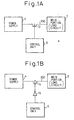
- Figs. 1A and 1B are diagrams illustrating conventional power line connection circuit using a MOS transistor.
- Fig. 1A illustrates an example of using an N-channel MOS transistor and
- Fig. 2B illustrates an example of using a P-channel MOS transistor.
- the same functional parts are denoted by the same reference numerals.
- reference numeral 4 denotes a power supply
- 5 denotes a main portion of a device which operates as a load circuit
- 6 denotes a control unit
- 200 denotes a power supply line
- 13 and 14 denotes power supply line switches, the switch 13 is an N-channel MOS transistor, and the switch 14 is a P-channel MOS transistor.
- 15 denotes an inverter which inverts a control signal.
- a signal at a positive voltage is fed from the control unit 6 to turn an N-channel MOS transistor 13 on, and a signal at ground voltage is fed from the control unit 6 to turn it off.
- a P-channel MOS transistor 14 is used, therefore, an inverter 15 for inverting the control signals must be provided if the control unit 6 outputs the same control signals as those of Fig. 1A.
- Fig. 2 is a circuit diagram illustrating an example of a conventional power line connection circuit using a power supply line switch.
- reference numeral 5 denotes a main portion of a device which operates a load circuit
- 16 denotes an N-channel MOS transistor which operates as the power line switch
- 41 denotes a power supply of 5V
- 42 denotes a power supply of 12V
- 61 denotes a control circuit
- 201 denotes a power supply line of 5V
- 202 denotes a power supply line of 12V.
- L1 denotes a voltage conversion circuit which converts a control signal of about 5V output from the control circuit 6 into a control signal of 12V.
- the control signal of 12V output from the voltage conversion circuit L1 is applied to a gate of the N-channel MOS transistor 16.
- a resistor R1 is a pull-down resistor which increases the operating speed of the control signal output from the control circuit 61.
- a capacitive element C1 is provided for stabilizing the output of the voltage conversion circuit L1. It is a well-known technique that capacitive elements such as capacitors are provided to stabilize a voltage of the power supply line 200 connected to the load 5. By using the capacitive elements, a stable voltage of the power supply can be obtained even when power consumption in the main portion fluctuates. A resistor R2 and the capacitive element C2 are used for this reason.
- the control signal applied to the gate of the N-channel MOS transistor 16 must satisfy the above-mentioned condition. Therefore, as shown in Fig. 2, the voltage conversion circuit L1 which converts the control signal into a signal having an appropriate voltage must be provided. Further, the power supply 42 of 12V must be provided for the voltage conversion circuit L1.
- Fig. 3 is a circuit diagram illustrating a constitution of a conventional power line connection circuit of a device in which power supply voltages supplied to some portions are switched between different voltages according to operational modes.
- a power supply 44 of 5V, a power supply 45 of 12V, an N-channel MOS transistor 18, a voltage conversion circuit L3, a load 51, resistors R4 and R5, and capacitive elements C4 and C5 respectively correspond to those of Fig. 2.
- the circuit shown in Fig. 3 further provides a power supply 43 of 3V and a power supply line switch using an N-channel MOS transistor 17 in the power supply line 204 to the load 51.
- a voltage conversion circuit L2 which converts a voltage of a control signal applied to a gate of the N-channel MOS transistor L2 is also provided.
- the control circuit 62 outputs control signals which turn either of the N-channel MOS transistors 17 and 18 on, or turn both of them off.
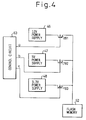
- Fig. 4 is a diagram illustrating a conventional power line connection circuit of an electrical erasable nonvolatile memory which is called a flash memory.
- the flash memories are divided into two types. In one type, 5V is supplied on the power supply line when stored data is read. In the other type, 3.3V is supplied on the power supply line when stored data is read. In both types, 12 V is supplied on the power supply line when data is written. 5V type is a normal type, and 3.3V type is a power conservation type. In a device using the flash memories, it is desired that either type of flash memories can be used. Therefore, as shown in Fig.
- a power supply 46 of 12V, a power supply 47 of 5V and a power supply 48 of 3.3V are provided, and a P-channel MOS transistor 191 and N-channel MOS typs transistors 192, 193 are provided on respective power supply lines to the flash memory 52.
- These transistors are controlled by control signals a, b and c output from the control circuit 63.
- the control signal a is “low” for write and erase operations, and it is “high (12V)” except the above operations.
- the control signal b is "high (12V)” when the flash memory 52 is accessed, and it is “low” while a standby mode.
- the control signal c is “high (12V)” when the flash memory 52 is accessed, and it is “low” while a standby mode.
- micro-processors automatically switch themselves to power conservation modes when the microprocessors do not operate for a predetermined time.
- power conservation modes power supplies are switched from 5V to 3.3V.
- the above power line connection circuits are used.
- Figs. 5A and 5B are diagrams illustrating the characteristic ON resistance of N-channel MOS transistor.
- Fig. 5A shows a circuit for measuring this characteristic
- Fig. 5B shows a characteristic measured by the circuit shown in Fig. 5A. From Fig. 5B, it is apparent that the ON resistance changes according to the power supply voltage Vs even when a constant voltage is applied to a gate of the transistor. Accordingly, when N-channel MOS transistors 17 and 18 shown in Fig. 3 have same characteristics, the ON resistances of those transistors are different. As described above, in the conventional circuits, the same ON resistances are obtained by using transistors having different characteristics or by adjusting output voltages of the voltage conversion circuits.
- a capacitive element is usually connected to stabilize the voltage of the power supply line 200.
- the power supply voltage is stably maintained against the fluctuation in the electric power consumed by the device unit.
- the capacitive element is connected, however, the voltage of the power supply line 200 gradually decreases when the switch 1 for the power supply lines is turned off due to the electric charge stored in the capacitive element, causing a problem of an increase in the erroneous operation in the device unit.
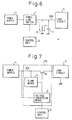
- Fig. 6 is a diagram illustrating a conventional constitution having a discharge circuit in which a resistor element is connected in parallel with a capacitive element in order to prevent the occurrence of erroneous operation.
- the circuit of Fig. 6 has a constitution in which a capacitor 7 and a discharge resistor 8 are connected to the circuit of Figs. 1A and 1B in order to stabilize the voltage of the power supply line 200.
- the electric charge stored in the capacitor 7 flows into a ground line through the resistor 8 as soon as the power line switch 1 is turned off, and the voltage of the power supply line 200 quickly drops.
- the discharge circuit shown in Fig. 6 has a problem in that a current flows at all times from the power supply line 200 to the ground line via the resistor 8 during the turned-on state.
- the resistor generally has a very large resistance, and the consumption of electric power due to the current flowing through the resistor is very small. However, such a consumption of electric power could become a serious problem in the devices which use batteries.
- the power supply circuits described above have heretofore been constituted by discrete circuits using power FETs. Therefore, these circuits have problems that the production costs are high. It has therefore been desired to reduce the size of the circuit and the cost of production by realizing the power line switches in the form of an IC.
- Fig. 7 is a diagram illustrating a fundamental constitution of the present invention.
- reference numeral 4 denotes a power supply
- 5 denotes a load circuit
- 6 denotes a control unit
- 10 denotes a MOS transistor
- 2 denotes a voltage conversion means
- 9 denotes a clamp means
- 200 denotes a power supply line.
- the clamp means 9 clamps the converted voltage output from the voltage conversion means 2 so as to have a predetermined voltage difference to a voltage of the power supply line 200. Therefore, even when the voltage of the power supply line 200 changes, the voltage difference between the gate and the drain of the MOS transistor 10 is constant. Therefore, assuming that the MOS transistor 10 is an N-channel type, the MOS transistor has a constant ON resistance when it is turned ON.
- the MOS transistor 10 When elements of the power line connection circuit are integrated into an IC, it is desired that elements in the area denoted by the reference numeral 100 are integrated. Namely, the MOS transistor 10, the voltage conversion means 2 and the clamp means 9 are preferably integrated.
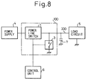
- reference numeral 1 denotes a power line switch; 4 denotes a power supply; 5 denotes a load circuit; 6 denotes a control unit; 7 denotes a capacitive element; 200 denotes a power supply line; and 3 denotes a discharge circuit.
- Fig. 9 is a diagram illustrating the constitution of the first embodiment of the present invention.
- reference numeral 11 denotes an N-channel MOS transistor; 4 denotes a power supply; 5 denotes a load circuit; 6 denotes a control unit; 21 denotes a charge pump circuit which boosts a control signal; 91 denotes a clamp circuit; and 200 denotes a power supply line.
- the charge pump circuit 21 corresponds to the voltage conversion means 2, and the clamp circuit 91 corresponds to the clamp means 9.
- the charge pump circuit 21 includes a ring oscillator 211; five diodes D1, D2, D3, D4, D5; four capacitive elements C1, C2, C3, C4; and two inverters INV1, INV2.
- the clamp circuit 91 includes a Zener diode Z1; a diode Db; and two PNP transistors Q1, Q2.
- the control circuit 6 When the N-channel MOS transistor 11 is turned on, the control circuit 6 outputs a control signal which has a voltage similar to the output voltage (5V) of the power supply 4. This control signal is applied to an anode of the diode D1 and to the ring oscillator 211. Then, the ring oscillator 211 starts to oscillate and outputs pulses. The pulses are input to the inverter INV1, and the output of the inverter INV1 is further input to the inverter INV2. In this way, complimentary pulses CK and /CK are generated. When CK is at low level, a voltage of a node N1 becomes about 5V, and the capacitive element C1 is charged to this voltage.
- the node N5 is connected to the power supply line 200 via the Zener diode Z1 , the diode Db, and the transistor Q1 or Q2. Therefore, even though the poetential of the node N5 is boosted by the charge pump circuit 21, it does not become higher than a sum of a potential of the power supply line 200, a threshold value VFZ1 of the Zener diode Z1, a threshold value VFDb of the diode Db, and a threshold value VBEPNP of the transistor Q1 or Q2. Namely, the voltage of the node N5 is higher than that of the power supply line 200 by VFZ1+VFDb+VBEPNP. This voltage is applied to a gate of the N-channel MOS transistor 11.
- the ON resistance of the MOS transistor is constant when the voltage difference between the gate and the power supply line is constant, the ON resistance of the MOS transistor of Fig. 9 is constant even when the voltage of the power supply line changes.
- the N-channel MOS transistor 11 turns off when the control signal output from the control circuit 6 is at low level. Generally, the OFF resistance of the N-channel MOS transistor is sufficiently high.
- the N-channel MOS transistor 11, the charge pump circuit 21 and the clamp circuit 91 are preferably integrated into the IC chip. However, either of the charge pump circuit 21 or the clamp circuit 91 may be integrated with the N-channel MOS transistor 11 into the IC.
- a P-channel MOS transistor can be used as a switch.
- a control signal of low level namely 0V signal is applied to the gate of the transistor in order to connect the load circuit to the power supply line, and a voltage higher than a power supply voltage by a predetermined value is applied to the gate in order to cut off the load circuit from the power supply line.
- the OFF resistance is made sufficiently large.
- the ON resistance becomes high but the size of the switch transistor is large.
- the circuit constitution can be simplified.
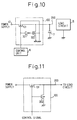
- Fig. 10 is a diagram illustrating the constitution of the first further power line connection circuit.
- reference numeral 121 denotes an N-channel MOS transistor which corresponds to the power line switch; 321 denotes an inverter; 322 denotes an N-channel MOS transistor which connects the power supply line 200 to a ground line; and 7 denotes a capacitor for stabilizing the voltage of the power supply line 200, which is connected between the power supply line 200 and the ground line.
- the two N-channel MOS transistors 121, 322 and the inverter 321 are formed inside the switch IC for power supply lines.
- the control signal from the control unit 6 is applied to the gate of the N-channel MOS transistor 121 as well as to the gate of the N-channel MOS transistor 322 via the inverter 321.
- the N-channel MOS transistor 121 is turned on, therefore, the N-channel MOS transistor 322 is turned off and, conversely, when the N-channel MOS transistor 121 is turned off, the N-channel MOS transistor 322 is turned on. It is possible to sufficiently increase the OFF resistance of the N-channel MOS transistor 322, so that a very small current flows from the power supply line 200 to ground even when the power supply voltage is applied to the power supply line 200.
- the electric charge of the capacitor 7 quickly flows to earth via the N-channel MOS transistor 322 reducing the probability of causing erroneous operation in the device unit 5.
- Fig. 11 is a diagram illustrating the constitution according to the second further power line connection circuit, wherein a P-channel MOS transistor 332 is provided instead of the N-channel MOS transistor 322 of Fig. 10, obviating the need of using the inverter.
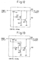
- Fig. 12 is a diagram illustrating the constitution according to the third further power line connection circuit, wherein a resistor 344 and an NPN transistor 343 are added to the circuit of Fig. 10.
- the NPN transistor 343 is turned on or off as the N-channel MOS transistor 342 is turned on or off.
- the current flows into earth more quickly than when the electric charge stored in the capacitor is discharged through the N-channel MOS transistor 322 of Fig. 4 only.
- Fig. 13 is a diagram illustrating the constitution according to the fourth further power line connection circuit, wherein a PNP transistor 355 is used as a transistor for discharging.
- the base of the PNP transistor 355 receives an output of a CMOS inverter circuit which is constituted by a P-channel MOS transistor 352 and an N-channel MOS transistor 353.
- the circuit is not able to lower the potential of the power supply line 200 down to ground potential (GND). Therefore, this embodiment should be used for such applications that do not develop trouble even under such a condition.
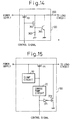
- Fig. 14 is a diagram illustrating the constitution according to the fifth further power line connection circuit, wherein a resistor 364 and an NPN transistor 364 are added to the circuit of Fig. 11. Similarly, therefore, the electric charge is quickly discharged through the NPN transistor 364.
- Fig. 15 is a diagram illustrating the constitution according to a second embodiment of the present invention, wherein the N-channel MOS transistor of the discharge circuit of the circuit of Fig. 10 is added to the constitution of the first embodiment that has the charge pump circuit and the clamp circuit of Fig. 9. This constitution makes it possible to obtain both of the effects explained in the foregoing.
- a switching IC for power supply lines for obtaining a desired ON resistance and a desired OFF resistance without requiring complex external circuit and a power line switch IC which quickly discharges the electric charge in the capacitive element for stabilizing the voltage of the power supply line when it is changed over to the off state and does not permit current to flow wastefully when it is in the on state.
Description
Claims (6)
- A power line connection circuit for controlling a connection of a power supply line (200) to a load circuit (5), comprising:characterized in thata MOS transistor (11) arranged in said power supply line (200), the continuity of said MOS transistor (11) being changed by applying a control signal output from a control unit (6) to a gate of said MOS transistor (11);a charge-pump circuit (21) for converting a voltage of said control signal; anda clamp means (9) for clamping said converted voltage output from said charge-pump circuit (21) so as to have a predetermined voltage difference with respect to the voltage of said power supply line (200),
said clamp means (9) discharges surplus power generated by said charge-pump circuit (21) to ground. - A power line connection circuit according to claim 1,
characterized in that
said clamp means (9) includes:a constant voltage drop circuit (Db, Z1), connected to said charge-pump circuit (21) and said gate of said MOS transistor (11) at a first end; anda bipolar junction transistor (Q2) having a collector connected to ground, an emitter connected to a second end of said constant voltage drop circuit (Db, Z1), and a base connected to a power supply line between said load circuit (5) and said MOS transistor (11). - A power line connection circuit according to claim 2,
characterized in that
said clamp means (9) further includes a second bipolar junction transistor (Q1) having a collector connected to ground, an emitter connected to said second end of said constant voltage drop circuit (Db, Z1), and a base connected to said power supply line (200). - A power line connection circuit according to any one of claims 1 to 3,
characterized by
a discharge circuit (3) which connects a node between said MOS transistor (11, 171) and said load circuit (5) to a ground line when said MOS transistor (11, 171) is turned off, and cuts off said node from said ground line when said MOS transistor (11, 171) is turned on. - A power line connection circuit according to any one of claims 1 to 4,
characterized in that
said MOS transistor (11) is of the N-channel type. - A switch IC for controlling a connection of a power supply line (200) to a load circuit (5), comprising a power line connection circuit according to any one of claims 1 to 5.
Applications Claiming Priority (2)
| Application Number | Priority Date | Filing Date | Title |
|---|---|---|---|
| JP12627193 | 1993-05-27 | ||
| JP126271/93 | 1993-05-27 |
Publications (3)
| Publication Number | Publication Date |
|---|---|
| EP0627807A2 EP0627807A2 (en) | 1994-12-07 |
| EP0627807A3 EP0627807A3 (en) | 1995-05-10 |
| EP0627807B1 true EP0627807B1 (en) | 1998-08-12 |
Family
ID=14931068
Family Applications (1)
| Application Number | Title | Priority Date | Filing Date |
|---|---|---|---|
| EP94108146A Expired - Lifetime EP0627807B1 (en) | 1993-05-27 | 1994-05-26 | Power line connection circuit and power line switch IC for the same |
Country Status (4)
| Country | Link |
|---|---|
| US (1) | US5650741A (en) |
| EP (1) | EP0627807B1 (en) |
| KR (1) | KR0161308B1 (en) |
| DE (1) | DE69412360T2 (en) |
Families Citing this family (17)
| Publication number | Priority date | Publication date | Assignee | Title |
|---|---|---|---|---|
| US5870573A (en) * | 1996-10-18 | 1999-02-09 | Hewlett-Packard Company | Transistor switch used to isolate bus devices and/or translate bus voltage levels |
| JP3378457B2 (en) * | 1997-02-26 | 2003-02-17 | 株式会社東芝 | Semiconductor device |
| TW423162B (en) * | 1997-02-27 | 2001-02-21 | Toshiba Corp | Power voltage supplying circuit and semiconductor memory including the same |
| KR100281336B1 (en) * | 1998-10-21 | 2001-03-02 | 구본준 | Shift register circuit |
| FR2837996A1 (en) * | 2002-03-29 | 2003-10-03 | Koninkl Philips Electronics Nv | MOS TRANSISTOR VOLTAGE CONVERTER |
| JP3902769B2 (en) * | 2003-08-29 | 2007-04-11 | 松下電器産業株式会社 | Step-down voltage output circuit |
| FR2874468B1 (en) * | 2004-08-17 | 2007-01-05 | Atmel Nantes Sa Sa | CURRENT DEVICE OF AT LEAST TWO VOLTAGES, CORRESPONDING ELECTRONIC CIRCUIT AND MEMORY |
| JP4440058B2 (en) | 2004-09-28 | 2010-03-24 | パナソニック株式会社 | Semiconductor integrated circuit |
| KR100571646B1 (en) * | 2005-03-31 | 2006-04-17 | 주식회사 하이닉스반도체 | Semiconductor device with power down mode |
| US7382168B2 (en) * | 2005-08-30 | 2008-06-03 | Agere Systems Inc. | Buffer circuit with multiple voltage range |
| US7436238B2 (en) * | 2006-02-13 | 2008-10-14 | Texas Instruments Deutschland Gmbh | Integrated voltage switching circuit |
| US7746154B2 (en) * | 2006-09-27 | 2010-06-29 | Atmel Corporation | Multi-voltage multiplexer system |
| US7849336B1 (en) * | 2007-04-17 | 2010-12-07 | Nvidia Corporation | Boost voltage generation |
| TWI451424B (en) * | 2009-04-17 | 2014-09-01 | Mstar Semiconductor Inc | Protecting circuit and power supply system for flash memory |
| JP5259505B2 (en) | 2009-06-26 | 2013-08-07 | 株式会社東芝 | Semiconductor memory device |
| TWI491124B (en) * | 2010-11-29 | 2015-07-01 | Hon Hai Prec Ind Co Ltd | Power supply adapter |
| JP6481553B2 (en) * | 2015-07-28 | 2019-03-13 | 株式会社デンソー | Switching element drive circuit |
Family Cites Families (27)
| Publication number | Priority date | Publication date | Assignee | Title |
|---|---|---|---|---|
| US3902078A (en) * | 1974-04-01 | 1975-08-26 | Crystal Ind Inc | Analog switch |
| US4316243A (en) * | 1979-12-17 | 1982-02-16 | General Electric Company | Power FET inverter drive circuit |
| US4420700A (en) * | 1981-05-26 | 1983-12-13 | Motorola Inc. | Semiconductor current regulator and switch |
| JPS5912622A (en) * | 1982-07-13 | 1984-01-23 | Toshiba Corp | Electronic switch circuit |
| USRE32526E (en) * | 1984-06-25 | 1987-10-20 | Gated solid state FET relay | |
| JPS6159911A (en) * | 1984-08-30 | 1986-03-27 | Nec Corp | Changeover switch circuit |
| GB8713384D0 (en) * | 1987-06-08 | 1987-07-15 | Philips Electronic Associated | Driving semiconductor device |
| GB8713388D0 (en) * | 1987-06-08 | 1987-07-15 | Philips Electronic Associated | Semiconductor device |
| IT1227561B (en) * | 1988-11-07 | 1991-04-16 | Sgs Thomson Microelectronics | CIRCUIT DEVICE, WITH REDUCED NUMBER OF COMPONENTS, FOR THE SIMULTANEOUS IGNITION OF A PLURALITY OF POWER TRANSISTORS |
| US4877982A (en) * | 1989-01-23 | 1989-10-31 | Honeywell Inc. | MOSFET turn-on/off circuit |
| FR2644651B1 (en) * | 1989-03-15 | 1991-07-05 | Sgs Thomson Microelectronics | INDUCTIVE LOAD POWER MOS TRANSISTOR CONTROL CIRCUIT |
| US4992683A (en) * | 1989-09-28 | 1991-02-12 | Motorola, Inc. | Load driver with reduced dissipation under reverse-battery conditions |
| US5023474A (en) * | 1989-11-08 | 1991-06-11 | National Semiconductor Corp. | Adaptive gate charge circuit for power FETs |
| JPH03158018A (en) * | 1989-11-15 | 1991-07-08 | Nec Corp | Input circuit |
| US5005061A (en) * | 1990-02-05 | 1991-04-02 | Motorola, Inc. | Avalanche stress protected semiconductor device having variable input impedance |
| US5111084A (en) * | 1990-05-31 | 1992-05-05 | Westinghouse Electric Corp. | Low loss drain pulser circuit for solid state microwave power amplifiers |
| KR930003929B1 (en) * | 1990-08-09 | 1993-05-15 | 삼성전자 주식회사 | Data output buffer |
| JP3028840B2 (en) * | 1990-09-19 | 2000-04-04 | 株式会社日立製作所 | Composite circuit of bipolar transistor and MOS transistor, and semiconductor integrated circuit device using the same |
| US5115143A (en) * | 1991-08-08 | 1992-05-19 | International Business Machines | Efficient P-channel FET drive circuit |
| FR2683687B1 (en) * | 1991-11-13 | 1994-03-04 | Nokia Consumer Electronics Franc | POWER SWITCH WITH MOS SWITCH. |
| US5258662A (en) * | 1992-04-06 | 1993-11-02 | Linear Technology Corp. | Micropower gate charge pump for power MOSFETS |
| US5365118A (en) * | 1992-06-04 | 1994-11-15 | Linear Technology Corp. | Circuit for driving two power mosfets in a half-bridge configuration |
| DE59308057D1 (en) * | 1992-08-04 | 1998-03-05 | Siemens Ag | Drive circuit for a power MOSFET with source-side load |
| JP3194798B2 (en) * | 1992-10-30 | 2001-08-06 | オリンパス光学工業株式会社 | Switch circuit with clamp function |
| US5321313A (en) * | 1993-01-07 | 1994-06-14 | Texas Instruments Incorporated | Controlled power MOSFET switch-off circuit |
| US5298817A (en) * | 1993-02-09 | 1994-03-29 | At&T Bell Laboratories | High-frequency solid-state relay |
| US5510747A (en) * | 1993-11-30 | 1996-04-23 | Siliconix Incorporated | Gate drive technique for a bidirectional blocking lateral MOSFET |
-
1994
- 1994-05-26 EP EP94108146A patent/EP0627807B1/en not_active Expired - Lifetime
- 1994-05-26 DE DE69412360T patent/DE69412360T2/en not_active Expired - Lifetime
- 1994-05-27 KR KR1019940011617A patent/KR0161308B1/en not_active IP Right Cessation
-
1996
- 1996-03-27 US US08/622,933 patent/US5650741A/en not_active Expired - Lifetime
Also Published As
| Publication number | Publication date |
|---|---|
| KR940027249A (en) | 1994-12-10 |
| DE69412360T2 (en) | 1999-04-22 |
| EP0627807A2 (en) | 1994-12-07 |
| EP0627807A3 (en) | 1995-05-10 |
| KR0161308B1 (en) | 1999-03-20 |
| DE69412360D1 (en) | 1998-09-17 |
| US5650741A (en) | 1997-07-22 |
Similar Documents
| Publication | Publication Date | Title |
|---|---|---|
| EP0627807B1 (en) | Power line connection circuit and power line switch IC for the same | |
| US5347170A (en) | Semiconductor integrated circuit having a voltage stepdown mechanism | |
| US6041011A (en) | Booster circuit and semiconductor memory device having the same | |
| EP0389566B1 (en) | Improved low power dual-mode cmos bias voltage generator | |
| US6801060B2 (en) | Semiconductor integrated circuit | |
| US6373325B1 (en) | Semiconductor device with a charge pumping circuit | |
| US6191615B1 (en) | Logic circuit having reduced power consumption | |
| US5420798A (en) | Supply voltage detection circuit | |
| KR100471185B1 (en) | Internal voltage converter scheme for controlling the power-up slope of internal supply voltage | |
| US7336108B2 (en) | Semiconductor integrated circuit with stepped-up voltage pump circuit | |
| US4806789A (en) | Power select circuit | |
| US4982113A (en) | Signal distributing unit for various input signals different in voltage level | |
| KR960004001B1 (en) | Single chip semiconductor memory | |
| US5278798A (en) | Semiconductor memory device | |
| JPH0241838B2 (en) | ||
| US6532178B2 (en) | Reducing level shifter standby power consumption | |
| JP3478596B2 (en) | Power supply connection circuit and power supply line switch IC | |
| US6157227A (en) | Device for neutralization in an integrated circuit | |
| JPH07261883A (en) | Semiconductor integrated circuit device for electric power control | |
| US4267465A (en) | Circuit for recharging the output nodes of field effect transistor circuits | |
| US6356488B1 (en) | Bias level generating circuit in a flash memory device | |
| US5353249A (en) | Non-volatile semiconductor memory device | |
| EP0748535B1 (en) | Improved supply voltage detection circuit | |
| US6650152B2 (en) | Intermediate voltage control circuit having reduced power consumption | |
| US5786686A (en) | Low-power consumption type semiconductor device |
Legal Events
| Date | Code | Title | Description |
|---|---|---|---|
| PUAI | Public reference made under article 153(3) epc to a published international application that has entered the european phase |
Free format text: ORIGINAL CODE: 0009012 |
|
| AK | Designated contracting states |
Kind code of ref document: A2 Designated state(s): DE FR GB |
|
| PUAL | Search report despatched |
Free format text: ORIGINAL CODE: 0009013 |
|
| AK | Designated contracting states |
Kind code of ref document: A3 Designated state(s): DE FR GB |
|
| 17P | Request for examination filed |
Effective date: 19950912 |
|
| 17Q | First examination report despatched |
Effective date: 19960308 |
|
| GRAG | Despatch of communication of intention to grant |
Free format text: ORIGINAL CODE: EPIDOS AGRA |
|
| GRAG | Despatch of communication of intention to grant |
Free format text: ORIGINAL CODE: EPIDOS AGRA |
|
| GRAH | Despatch of communication of intention to grant a patent |
Free format text: ORIGINAL CODE: EPIDOS IGRA |
|
| GRAH | Despatch of communication of intention to grant a patent |
Free format text: ORIGINAL CODE: EPIDOS IGRA |
|
| GRAA | (expected) grant |
Free format text: ORIGINAL CODE: 0009210 |
|
| AK | Designated contracting states |
Kind code of ref document: B1 Designated state(s): DE FR GB |
|
| REF | Corresponds to: |
Ref document number: 69412360 Country of ref document: DE Date of ref document: 19980917 |
|
| ET | Fr: translation filed | ||
| PLBE | No opposition filed within time limit |
Free format text: ORIGINAL CODE: 0009261 |
|
| STAA | Information on the status of an ep patent application or granted ep patent |
Free format text: STATUS: NO OPPOSITION FILED WITHIN TIME LIMIT |
|
| 26N | No opposition filed | ||
| REG | Reference to a national code |
Ref country code: GB Ref legal event code: IF02 |
|
| REG | Reference to a national code |
Ref country code: GB Ref legal event code: 732E Free format text: REGISTERED BETWEEN 20090305 AND 20090311 |
|
| REG | Reference to a national code |
Ref country code: FR Ref legal event code: TQ |
|
| REG | Reference to a national code |
Ref country code: FR Ref legal event code: CD Ref country code: FR Ref legal event code: CA |
|
| PGFP | Annual fee paid to national office [announced via postgrant information from national office to epo] |
Ref country code: GB Payment date: 20130619 Year of fee payment: 20 Ref country code: DE Payment date: 20130626 Year of fee payment: 20 |
|
| REG | Reference to a national code |
Ref country code: DE Ref legal event code: R082 Ref document number: 69412360 Country of ref document: DE Representative=s name: VON KREISLER SELTING WERNER - PARTNERSCHAFT VO, DE Effective date: 20130718 Ref country code: DE Ref legal event code: R082 Ref document number: 69412360 Country of ref document: DE Representative=s name: VON KREISLER SELTING WERNER, DE Effective date: 20130718 Ref country code: DE Ref legal event code: R082 Ref document number: 69412360 Country of ref document: DE Representative=s name: MITSCHERLICH & PARTNER PATENT- UND RECHTSANWAE, DE Effective date: 20130718 Ref country code: DE Ref legal event code: R081 Ref document number: 69412360 Country of ref document: DE Owner name: SPANSION LLC (N.D.GES.D. STAATES DELAWARE), SU, US Free format text: FORMER OWNERS: FUJITSU SEMICONDUCTOR LTD., YOKOHAMA, KANAGAWA, JP; KYUSHU FUJITSU ELECTRONICS LTD., KAGOSHIMA, JP Effective date: 20130718 Ref country code: DE Ref legal event code: R081 Ref document number: 69412360 Country of ref document: DE Owner name: SPANSION LLC (N.D.GES.D. STAATES DELAWARE), US Free format text: FORMER OWNER: FUJITSU SEMICONDUCTOR LTD., KYUSHU FUJITSU ELECTRONICS LTD., , JP Effective date: 20130718 Ref country code: DE Ref legal event code: R081 Ref document number: 69412360 Country of ref document: DE Owner name: FUJITSU SEMICONDUCTOR LTD., JP Free format text: FORMER OWNER: FUJITSU SEMICONDUCTOR LTD., KYUSHU FUJITSU ELECTRONICS LTD., , JP Effective date: 20130718 |
|
| REG | Reference to a national code |
Ref country code: FR Ref legal event code: TQ Owner name: FUJITSU SEMICONDUCTOR LIMITED, JP Effective date: 20130911 Ref country code: FR Ref legal event code: TP Owner name: FUJITSU SEMICONDUCTOR LIMITED, JP Effective date: 20130911 |
|
| REG | Reference to a national code |
Ref country code: GB Ref legal event code: 732E Free format text: REGISTERED BETWEEN 20131017 AND 20131023 |
|
| PGFP | Annual fee paid to national office [announced via postgrant information from national office to epo] |
Ref country code: FR Payment date: 20130719 Year of fee payment: 20 |
|
| REG | Reference to a national code |
Ref country code: GB Ref legal event code: 732E Free format text: REGISTERED BETWEEN 20131114 AND 20131120 |
|
| REG | Reference to a national code |
Ref country code: FR Ref legal event code: TP Owner name: SPANSION LLC, US Effective date: 20140109 |
|
| REG | Reference to a national code |
Ref country code: DE Ref legal event code: R082 Ref document number: 69412360 Country of ref document: DE Representative=s name: VON KREISLER SELTING WERNER, DE |
|
| REG | Reference to a national code |
Ref country code: DE Ref legal event code: R082 Ref document number: 69412360 Country of ref document: DE Representative=s name: VON KREISLER SELTING WERNER - PARTNERSCHAFT VO, DE Effective date: 20140331 Ref country code: DE Ref legal event code: R081 Ref document number: 69412360 Country of ref document: DE Owner name: SPANSION LLC (N.D.GES.D. STAATES DELAWARE), SU, US Free format text: FORMER OWNER: FUJITSU SEMICONDUCTOR LTD., YOKOHAMA, KANAGAWA, JP Effective date: 20140331 Ref country code: DE Ref legal event code: R081 Ref document number: 69412360 Country of ref document: DE Owner name: SPANSION LLC (N.D.GES.D. STAATES DELAWARE), US Free format text: FORMER OWNER: FUJITSU SEMICONDUCTOR LTD., YOKOHAMA, JP Effective date: 20140331 |
|
| REG | Reference to a national code |
Ref country code: DE Ref legal event code: R071 Ref document number: 69412360 Country of ref document: DE |
|
| REG | Reference to a national code |
Ref country code: DE Ref legal event code: R071 Ref document number: 69412360 Country of ref document: DE |
|
| REG | Reference to a national code |
Ref country code: GB Ref legal event code: PE20 Expiry date: 20140525 |
|
| PG25 | Lapsed in a contracting state [announced via postgrant information from national office to epo] |
Ref country code: GB Free format text: LAPSE BECAUSE OF EXPIRATION OF PROTECTION Effective date: 20140525 |
|
| PG25 | Lapsed in a contracting state [announced via postgrant information from national office to epo] |
Ref country code: DE Free format text: LAPSE BECAUSE OF EXPIRATION OF PROTECTION Effective date: 20140527 |
|
| REG | Reference to a national code |
Ref country code: GB Ref legal event code: 732E Free format text: REGISTERED BETWEEN 20150625 AND 20150701 |