EP0623249B1 - Connector having plate-type internal shielding - Google Patents
Connector having plate-type internal shielding Download PDFInfo
- Publication number
- EP0623249B1 EP0623249B1 EP93904394A EP93904394A EP0623249B1 EP 0623249 B1 EP0623249 B1 EP 0623249B1 EP 93904394 A EP93904394 A EP 93904394A EP 93904394 A EP93904394 A EP 93904394A EP 0623249 B1 EP0623249 B1 EP 0623249B1
- Authority
- EP
- European Patent Office
- Prior art keywords
- shielding member
- contact elements
- connector
- another
- assembly according
- Prior art date
- Legal status (The legal status is an assumption and is not a legal conclusion. Google has not performed a legal analysis and makes no representation as to the accuracy of the status listed.)
- Expired - Lifetime
Links
- 230000013011 mating Effects 0.000 claims abstract description 11
- 239000000463 material Substances 0.000 claims description 10
- 210000003739 neck Anatomy 0.000 description 6
- 238000010276 construction Methods 0.000 description 3
- PCHJSUWPFVWCPO-UHFFFAOYSA-N gold Chemical compound [Au] PCHJSUWPFVWCPO-UHFFFAOYSA-N 0.000 description 3
- 239000010931 gold Substances 0.000 description 3
- 229910052737 gold Inorganic materials 0.000 description 3
- 238000005452 bending Methods 0.000 description 1
Images


Classifications
-
- H—ELECTRICITY
- H01—ELECTRIC ELEMENTS
- H01R—ELECTRICALLY-CONDUCTIVE CONNECTIONS; STRUCTURAL ASSOCIATIONS OF A PLURALITY OF MUTUALLY-INSULATED ELECTRICAL CONNECTING ELEMENTS; COUPLING DEVICES; CURRENT COLLECTORS
- H01R13/00—Details of coupling devices of the kinds covered by groups H01R12/70 or H01R24/00 - H01R33/00
- H01R13/648—Protective earth or shield arrangements on coupling devices, e.g. anti-static shielding
- H01R13/658—High frequency shielding arrangements, e.g. against EMI [Electro-Magnetic Interference] or EMP [Electro-Magnetic Pulse]
- H01R13/6581—Shield structure
- H01R13/6585—Shielding material individually surrounding or interposed between mutually spaced contacts
-
- H—ELECTRICITY
- H01—ELECTRIC ELEMENTS
- H01R—ELECTRICALLY-CONDUCTIVE CONNECTIONS; STRUCTURAL ASSOCIATIONS OF A PLURALITY OF MUTUALLY-INSULATED ELECTRICAL CONNECTING ELEMENTS; COUPLING DEVICES; CURRENT COLLECTORS
- H01R12/00—Structural associations of a plurality of mutually-insulated electrical connecting elements, specially adapted for printed circuits, e.g. printed circuit boards [PCB], flat or ribbon cables, or like generally planar structures, e.g. terminal strips, terminal blocks; Coupling devices specially adapted for printed circuits, flat or ribbon cables, or like generally planar structures; Terminals specially adapted for contact with, or insertion into, printed circuits, flat or ribbon cables, or like generally planar structures
- H01R12/50—Fixed connections
- H01R12/51—Fixed connections for rigid printed circuits or like structures
- H01R12/52—Fixed connections for rigid printed circuits or like structures connecting to other rigid printed circuits or like structures
-
- H—ELECTRICITY
- H01—ELECTRIC ELEMENTS
- H01R—ELECTRICALLY-CONDUCTIVE CONNECTIONS; STRUCTURAL ASSOCIATIONS OF A PLURALITY OF MUTUALLY-INSULATED ELECTRICAL CONNECTING ELEMENTS; COUPLING DEVICES; CURRENT COLLECTORS
- H01R12/00—Structural associations of a plurality of mutually-insulated electrical connecting elements, specially adapted for printed circuits, e.g. printed circuit boards [PCB], flat or ribbon cables, or like generally planar structures, e.g. terminal strips, terminal blocks; Coupling devices specially adapted for printed circuits, flat or ribbon cables, or like generally planar structures; Terminals specially adapted for contact with, or insertion into, printed circuits, flat or ribbon cables, or like generally planar structures
- H01R12/70—Coupling devices
- H01R12/71—Coupling devices for rigid printing circuits or like structures
- H01R12/72—Coupling devices for rigid printing circuits or like structures coupling with the edge of the rigid printed circuits or like structures
- H01R12/73—Coupling devices for rigid printing circuits or like structures coupling with the edge of the rigid printed circuits or like structures connecting to other rigid printed circuits or like structures
Definitions
- the invention relates to an electrical connector assembly, comprising a plug connector and a socket connector mating therewith, which plug connector and socket connector can be pushed into one another, which plug connector is provided with at least two rows of terminal connections which are accommodated in a first plastic housing and at least one row of which consists of male terminal pins, and which socket connector is provided with at least two rows of terminal connections which are accommodated in a second plastic housing and at least one row of which consists of female terminal connections, one male terminal pin always being in electrically conducting contact with a female terminal connection when plug connector and socket connector are pushed into one another, the plug connector being provided with at least one electrically conducting first shielding member arranged between said rows of terminal connections in the plug connector and being rigidly accommodated in the first housing, the socket connector being provided with at least one conducting second shielding member arranged between said rows of terminal connections in the socket connector and being rigidly accommodated in a second housing and comprising at least one resilient contact element, which first shielding member and second shielding member make electrically conducting contact with one another when the plug connector
- Such a connector assembly is disclosed by the International Patent Application WO 88.04484.
- the plug connector comprises two rows of male terminal pins which are able to mate with two rows of female terminal connections of the socket connector. Between the two rows of male terminal pins in the housing of the plug connector there is accommodated at least one plate-type shielding member.
- a shielding member Accommodated between the two rows of female terminal connections in the housing of the socket connector is also a shielding member which has a female structure with sprung lips which grip round the plate-type shielding member of the plug connector if the plug connector is connected to the socket connector.
- the shielding members may optionally be used for power supply or may be set to a predetermined voltage, for example ground.
- a shielding plate and a female shielding member may be provided alongside one another, which combinations can each supply their own voltage or current.
- a disadvantage of the known device is that the shielding plate in the plug connector is not resilient and is relatively thick. As a result, the combination of a shielding consisting of a shielding plate which is accommodated in a gripping manner in a female shielding member of a socket connector takes up a relatively large amount of space. This obstructs further miniaturisation.
- the object of the invention is to construct the entire shielding, consisting of the combination of a shielding member in both the plug connector and the socket connector in such a way that it can be miniaturised further.
- a connector assembly according to the invention is characterized in that each said contact element of each said first shielding member within the plug connector is a resilient, flat contact element and in that each said contact element of the second shielding member within the socket connector is a resilient, flat contact element, in such a way that when the socket connecter and the plug connecter are connected to each other each contact element of the first shielding member is slid along at least one contact element of the second shielding member.
- the shielding combination no longer needs two different types of shielding member, namely one having a stiff male part and one female part provided with lips situated opposite one another and the shielding members both in the plug connector and in the socket connector can be made of very thin, simply constructed, conducting plate material and the space required for the entire shielding is substantially less than in the known device.
- the connector assembly according to the invention is characterized in that the first shielding member is provided with an elongated support to support each resilient contact element wherein each contact element is connected to the support via a narrow neck providing the resilient action.
- the connector assembly according to the invention is characterized in that the second shielding member is provided with an elongated support to support each resilient contact element wherein each contact element is connected to the support via a narrow neck providing the resilient action.
- the connector assembly according to the invention is characterized in that the first shielding member comprises several contact elements which are arranged alongside one another and consist of alternately closed contact elements and open contact elements, the latter being provided with at least two lips.
- the connector assembly according to the invention is characterized in that the second shielding member comprises several contact elements which are arranged alongside one another and consist of alternately closed contact elements and open contact elements, the latter being provided with at least two lips.
- the connector assembly according to the invention is characterized in that, when the plug connector and the socket connector are connected to one another, closed contact elements are always situated opposite open contact elements.
- the connector assembly according to the invention is characterized in that the first shielding member comprises several closed contact elements situated alongside one another.
- the connector assembly according to the invention is characterized in that the second shielding member comprises several closed contact elements situated alongside one another.
- the connector assembly according to the invention is characterized in that the first shielding member comprises several closed contact elements situated alongside one another and the second shielding member comprises several open contact elements situated alongside one another, and when the plug connector and the socket connector are connected to one another, each closed contact element is situated opposite an open contact element.
- the connector assembly according to the invention is characterized in that the second shielding member comprises several closed contact elements situated alongside one another and the first shielding member comprises several open contact elements situated alongside one another, and when the plug connector and the socket connector are connected to one another, each closed contact element is situated opposite an open contact element.
- the connector assembly according to the invention is characterized in that the second shielding member comprises several closed contact elements situated alongside one another and the first shielding member comprises several closed contact elements situated alongside one another, and when the plug connector and the socket connector are connected to one another, the closed contact elements of the second shielding member close off the opening between two adjacent, oppositely situated closed contact elements of the first shielding member and the closed contact elements of the first shielding member close off the opening between two adjacent, oppositely situated closed contact elements of the second shielding member.
- the connector assembly according to the invention is characterized in that the ends of adjacent contact elements of both the first and the second shielding member are to some extent bent, turn and turn about, to an oppositely facing side as seen in the connected state of the socket connector and the plug connector.
- This embodiment has the advantage that the internal stresses in the two shielding members which occur when a plug connector is connected to a socket connector are compensated for.
- the connector assembly according to the invention is characterized in that the first shielding member is made of conducting plate material approximately 0.15 mm thick.
- the connector assembly according to the invention is characterized in that the second shielding element is made of conducting plate material approximately 0.15 mm thick.
- the invention relates to a plug connector of a connector assembly defined above, provided with at least two rows of terminal connections which are accommodated in a first plastic housing, at least one row of which consisting of male terminal pins, and at least one electrically conducting first shielding member arranged between said rows of terminal connections in the plug connector and being rigidly accommodated in the first housing, characterized in that each said contact element of each said first shielding member within the plug connector is a resilient, flat contact element.
- the invention relates to a socket connector of a connector assembly defined above, provided with at least two rows of terminal connections which are accommodated in a second plastic housing, at least one row of which consisting of female terminal connections, and at least one conducting shielding member arranged between said rows of terminal connections in the socket connector and being rigidly accommodated in a second housing and comprising at least one resilient contact element, characterized in that each said contact element of each said second shielding member within the socket connector is a resilient, flat contact element.
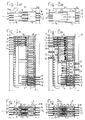
- FIGS 1a, b and c show a connector 1 provided with female terminal connections 10; this connector is referred to below as “socket connector”.
- the female terminal connections 10 clamp round male terminal pins 4 of the connector 2 which mates therewith and which will be referred to below as "plug connector”.
- the plug connector 1 is always provided with two parallel rows of male terminal pins 4, but that it is always possible to replace one row thereof by a row of female terminal connections 10.
- the plug connector 1 is possible, furthermore, to accommodate more than two rows of terminal connections in both the plug connector and the socket connector, with a shielding member between all the rows or between some of the rows.
- Every female terminal connection 10 leads, via feed-through 3 (or 11) to a printed circuit board 7 for electrical connection to other circuit elements (not shown).
- Every female terminal connection 10 has one feed-through 3 or 11: if, viewed in the longitudinal direction ( Figure 1b), a particular terminal connection 10 has a feed-through 3, then the adjacent terminal connection 10 has a feed-through 11 which, viewed in cross section, is closer to the centre of the connector ( Figure 1c) than the feed-through 3.
- the female terminal connections 10 are rigidly accommodated in a plastic housing 6. The end consists of two sprung lips which are able to clamp rigidly around a male terminal pin 4 of a plug connector 2 in order, in this way, to make a rigid electrically conducting contact. In the width of the socket connector 2 there is room for two parallel rows of female terminal connections 10 (Figure 1c).
- Every male terminal pin 4 is led further via a feed-through 9, 12 to a printed circuit board 8 for electrical connection to other circuit elements (not shown).
- the male terminal pins 4 are rigidly accommodated in a plastic housing 5.
- the plastic housing 5 of the plug connector 2 comprises two walls 13 which grip round the housing 6 of the socket connector 1.
- the feed-throughs 9 and 12 are alternately fitted closer to, and further away from, the centre line in the cross section of the plug connector 1. In the width of the plug connector 1, there is always sufficient room for two adjacently situated rows of male terminal pins 4 (Figure 2c).
- the spacing xl between the printed circuit board 7 and the printed circuit board 8 is preferably 9.6 mm.
- the thickness x2 of the printed circuit board 7 or 8 is, for example, 1.6 mm.
- FIGs 2a, b and c show socket connector 1 and plug connector 2 which grip into one another and which are both provided, according to the invention, with a shielding plate 14 and 15, respectively. If the socket connector 1 and the plug connector 2 are rigidly pushed against one another, the shielding plates 14 and 15, respectively, make electrically conducting contact and in this way form an electromagnetic shielding against crosstalk between one row of connections (for example the uppermost row in Figure 2c) and the other row of connections (the lowermost row in Figure 2c).
- the shielding plate 14 leads via a feed-through 16 through the printed circuit board 7, while the shielding plate 15 is lead via a feed-through 17 through printed circuit board 8. Via the feed-through 16 or 17 the shielding plate 14 or 15, respectively, can be set to a predetermined voltage, for example ground potential.
- the shielding plate can also be set, for example, to the supply voltage.
- the spacing x3 between the printed circuit boards 7 and 8 is equal to the spacing x1 in Figure 1a and is therefore, preferably, 9.6 mm.
- the thickness x4 of the printed circuit boards 7 and 8 is equal to x2 in Figure la and is therefore also, for example, 1.6 mm.
- FIG 3 shows Figure 2b enlarged.
- the shielding plate 15 comprises an elongated support 22.
- On one side of the support 22 there extend alternately different contact elements 18 and 19 which are connected by a thin neck 26, 27 to the support 22.
- the necks 26, 27 are so thin that the contact elements 18 and 19 are able to spring with respect to the support 22 in a direction perpendicular to the plane of the drawings of Figure 3.
- the contact element 18 is completely closed, whereas the contact element 19 is provided with two lips 20, 21 which form an opening in between.
- dimples 23, 24 Provided on the ends of the lips 20, 21 are dimples 23, 24.
- the contact elements 18, 19 are, as stated, constructed in such a way that they can spring perpendicularly to the plane of the drawing of Figure 3.
- small projections 44 against which the contact elements rest, are accommodated between adjacent contact elements 18, 19 in the wall of the housing.
- elongated projections 43 which fulfil the same function as the small projections 44 mentioned above can be accommodated in the wall of the housing.
- Both the small projections 44 and the projections 43 also have a second function; they also rest against the support 22 of the shielding plate 14 and thereby prevent the shielding plate from being able to move within the housing when the feed-throughs 16 of the shielding plate are pushed into openings, intended therefore, in the printed circuit board 7.
- the projections 43 project outwards to such an extent inside the socket connector 1 that they rest precisely against a small projection 44 between two adjacent contact elements 18, 19 of a plug connector 2 when the socket connector 1 is connected to the plug connector 2.
- the plug connector 2 may also contain some elongated projection 43 of this type. These latter are not shown in the Figure but are not, of course, situated opposite the projections 43 in the housing of the socket connector 1.
- All the open contact elements 19 may be provided with a notch 45 in the portion connecting the two lips 20, 21 to one another. Notch 45 mates with a rib 46 in the wall of the housing of the respective connector in order to simplify location of the shielding plate in the connector.
- the shielding plate 14 accommodated in the socket connector 1 is identical to the shielding plate 15 of the plug connector 2.
- the shielding plates 14 and 15 are placed in the longitudinal direction in the socket connector 1 or plug connector 2, respectively, in such a way that a closed contact element 18 always appears opposite an open contact element 19. Variants of this are possible as will be explained below by reference to Figures 14 to 17 inclusive.
- both the closed contact element 18 and the open contact element 19 are constructed so as to spring with respect to the support 22.
- the last-mentioned thickness of the plate material used is preferably 0.15 mm. All this will become clearer by reference to Figure 4 which is an enlarged version of Figure 2c. It can clearly be seen that, when socket connector and plug connector are pushed into one another, the shielding plate 14 of the socket connector 1 is in contact with the shielding plate 15 of the plug connector 2.
- a closed contact element 18 (not shown) in the socket connector 1, which closed contact element 18 can bend aside somewhat further in its own funnel-shaped opening 25 than the open contact element 19, mating therewith, of the plug connector 2.
- the total thickness which the plate-type shielding requires at the position of the contact between an open and a closed contact element is twice the thickness of the plate material used for the contact elements (preferably, 0.15 mm thick) plus twice the space which is needed for a bent end of each of the shielding plates 14, 15.
- Figures 5 to 8 inclusive show an individual male plug connector 2 according to the invention in various views.
- Figure 5 shows a plan view of a plug connector 2.
- the connector 2 contains two rows of 21 male terminal pins 4. This number is only an example. Between the two rows there is a shielding plate of alternately closed and open contact elements 18, 19. All the contact elements 18, 19 are able to make electrical contact with one another via a support 22 ( Figure 3). It is also possible, however, that the support 22 is cut through between two adjacent contact elements and the shielding consists of electrically separated sections each having their own voltage.
- Figure 5 shows four pairs of open and closed contact elements 18, 19. Another number is, however, possible within the scope of the invention.
- the wall 13 has an opening 28 for mating with a projection 29 of the socket connector 1, while the other lip 13 has at its ends openings 30, 31 for mating with projections 32, 33 of the socket connector 1 (see Figure 9).
- Figure 6 shows a separate plug connector 2 in cross section, the reference numerals being the same as in Figure 4.
- Figure 6 also reveals another characteristic of the present invention.
- the support 22 of the shielding plate is situated in an opening 35 of the housing 5. Because the support is provided with protuberances 36, 37 and 38, the shielding cannot, however, easily be moved to and fro through the opening 35 of the housing 5.
- the protuberances 36, 37, 38 the openings 35 can be wider than the thickness of the plate material used for the shielding.
- the end of the contact element 18, 19 can be bent, after which the entire shielding 14, 15 is pushed through the opening 35. In practice, that is done from the bottom of the connector that is to say in the plane of the drawing seen from right to left.
- Figure 6 requires no further explanation.
- Figure 7 shows a side view of the plug connector 2 in which some preferred dimensions are included.
- the height x5 of the connector is preferably 7.4 mm, the height x6 to which the terminal pins project 2.5 mm, the height x7 of the base of the housing 5 3.4 mm, the spacing x8 between the feed-through 17 of the shielding and the closest feed-through 12 of a terminal pin 4 in lateral projection 0.75 mm, the spacing x9 between two adjacent feed-throughs 9 and 12 of terminal pins 4 in lateral projection 1.0 mm, the thickness x10 of a terminal pin 0.4 mm, and the width x11 of the housing 4.5 mm.
- other dimensions are possible within the scope of the invention.
- Figure 8 shows a cutaway longitudinal view of a separate plug connector 2 according to the invention. After Figure 4, this figure does not require a separate explanation.
- Figure 9 shows a plan view of a socket connector according to the invention. Two rows, each of 21 female terminal connections 10, are shown, which rows are separated by a shielding plate provided with four pairs of alternating contact elements 18, 19. The numbers shown here have been arbitrarily chosen and can also be different within the scope of the invention.
- the projections 29, 32 and 33 are provided to mate with the openings 28, 30 and 31 of the plug connector ( Figure 5). Of course, the dimensions of the socket connector are furthermore such that each female terminal connection 10 is able to mate with a male terminal pin 4 of a plug connector.
- the closed and open contact elements 18, 19 are so positioned that, when a plug connector and a socket connector are brought into contact, an open contact element 19 always ends up opposite a closed contact element 18, after which they come into contact with one another in a sliding manner and both are also bent to some extent in a sprung manner, as explained above.
- Figure 9 shows some dimensions which, of course, also apply to the corresponding dimensions of the plug connector of Figure 5.
- the width x12 of the socket connector 1 is 3.5 mm
- the spacing x13 between the shielding plate and the centres of the female terminal connections 10 1.0 mm the spacing x14 between the centreline of the two rows of female terminal connections 10 2.0 mm
- the total length x19 of the socket connector 1 21.5 mm the length x16 of the projections 32 and 33 1.0 mm
- the spacing x17 between the centre of the projection 29 at the edge 10.75 mm and the spacing x18 between two adjacent female terminal connections 1.0 mm.
- FIG 10 shows a socket connector according to the invention in cross section.
- the funnel-shaped opening 25 can be clearly seen and is intended for the bending-aside of the contact element 19 (or 18) if the socket connector 1 is pushed into a plug connector 2 and the contact element 19 (or 18) comes into sliding contact with an oppositely situated contact element 18 (or 19) of the shielding plate 15 of the plug connector 2.
- the shielding plate 14 is led through an opening 39 of the housing 6 in the same way as the shielding plate 15 in Figure 6 after the end of the contact element 19 (or 18) has been bent.
- the opening 39 is wider than the thickness of the plate material used for the shielding plate.
- Protuberances 40, 41 and 42 have the same function as the protuberances 36, 37 and 38 in Figure 6.
- the completely finished shielding plate 14 is pushed from left to right through the opening 39 of the housing 6 in the plane of the drawing in Figure 10. In other respects, Figure 10 requires no further explanation after Figure 4.
- Figure 11 shows a side view of a socket connector 1.
- the width x12 of the socket connector (cf. Figure 9) is 3.5 mm, while the width, inclusive of the projections 29 and 32/33 (x20) is 4.3 mm.
- the spacings x21 and x22 correspond to the spacings x9 and x8, respectively, of Figure 7.
- the height x23 of the projection 29, 32 and 33 is 2.25 mm.
- these dimensions are again also examples of an embodiment of the invention and they are not intended to limit it.
- Figure 12 shows a separate, cutaway socket connector 1 in the longitudinal direction.
- the reference numerals are identical to those which have also been used in Figure 4, so that Figure 12 requires no separate explanation.
- FIGs 13a to d inclusive show separate strip-type shieldings 14, 15 according to the invention.
- the shielding plates 14 and 15 are identical and can be made with one die.
- each shielding plate consists of a support 22 which has on its one side feed-throughs 17 for feeding through a printed circuit board.
- alternately closed contact elements 18 and open contact elements 19 which are bent to some extent at their end ( Figure 13b and d).
- the ends of the open contact elements consist of two lips 20, 21 which are each provided with a small dimple 23, 24.
- a rib can be provided which mates with a small notch 34 in the opening of the open contact element 19 so that the open contact element 19 is satisfactorily held in the correct position.
- Figure 13c shows some dimensions for explaining the shielding plate according to the invention.
- the centre-to-centre spacing x24 between two adjacent contact elements 18 and 19 is 2.5 mm.
- the spacing x25 between two adjacent feed-throughs 17 may also be 2.5 mm, but may be chosen independently of the spacing x24.
- the spacing x24 can also be freely chosen with respect to the spacing between adjacent terminal pins 4 or adjacent terminal connections 10.
- the centre-to-centre spacing x26 between the necks 26, 27 of two adjacent contact elements 18, 19 is, for example, also 2.5 mm but this does not necessarily have to be equal to the centre-to-centre spacing x24 between two adjacent contact elements 18 and 19.
- Figures 13b and d once again show clearly the protuberances 40, 41 and 42 in the support 22 of a shielding plate which mate with an opening 39 (or 35) of the connector in which the shielding plate is positioned.
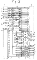
- Figures 14a and b show a first variant of the shielding plates 14, 15 as shown in Figures 13a and b.
- the shielding plate 14, 15 of both Figure 14a and of Figure 14b comprises only closed contact elements.
- the contact elements 18 of Figure 14b are identical to those of Figure 13, while the contact elements 18' of Figure 14a are provided with small dimples 23', 24' which have the same function as the small dimples 23, 24 which are provided on the lips 20, 21 of an open contact element 19.
- the shielding plates 14, 15 of Figures 14a and b can be made with the same die. After that, the contact elements 18' of half the still identical shielding plates 14, 15 made in this way have to be provided with small dimple 23', 24'.
- Characteristic of the embodiment of Figures 14a and b is, furthermore, that one shielding plate 14, 15 having contact elements 18, for example provided in a plug connector 2, is positioned opposite a shielding plate 14, 15, mating therewith, provided with contact elements 18', provided in a socket connector 1 in such a way that the contact elements 18 and 18' end up precisely opposite one another.
- all the plug connectors 2 are provided with shielding plates 14, 15 having contact elements 18' and all the socket connectors 1 with shielding plates 14, 15 having contact elements 18.
- shielding plates 14, 15 which has only open contact elements 19 and one type of shielding plates 14, 15 which has only closed contact elements 18, as is explained in Figures 15a and b.
- the small dimples 23, 24 are then provided in the lips 20, 21 of the open contact elements, although it is possible to provide them instead thereof on the closed contact elements 18.
- the shielding plates 14, 15 are again positioned in a plug connector and a socket connector in such a way that an open contact element 19 always appears precisely opposite a closed contact element 18 one connects a plug connector to a socket connector.
- the shielding plate 14, 15 having closed contact elements 18' is situated in its connector (plug connector or socket connector) offset in such a way with respect to the shielding plate 14, 15 having closed contact elements 18 in the connector mating therewith (socket connector or plug connector) that if the two connectors are connected to one another, the contact elements 18 and 18', respectively, completely close off the slit between oppositely situated contact elements 18' and 18, respectively.
- all the faces of the contact elements 18, 18', 19 in a connector which come into contact with mating contact elements 18, 18', 19 in another connector can be provided with a thin gold layer.
- a thin gold layer on one side of the different contact elements is sufficient.
- such a thin gold layer has to be provided on two sides of the contact elements or turn and turn about on a different side in adjacent contact elements because the contact elements always make contact turn and turn about at their other side with another contact element.
Landscapes
- Details Of Connecting Devices For Male And Female Coupling (AREA)
Abstract
Description
- The invention relates to an electrical connector assembly, comprising a plug connector and a socket connector mating therewith, which plug connector and socket connector can be pushed into one another, which plug connector is provided with at least two rows of terminal connections which are accommodated in a first plastic housing and at least one row of which consists of male terminal pins, and which socket connector is provided with at least two rows of terminal connections which are accommodated in a second plastic housing and at least one row of which consists of female terminal connections, one male terminal pin always being in electrically conducting contact with a female terminal connection when plug connector and socket connector are pushed into one another, the plug connector being provided with at least one electrically conducting first shielding member arranged between said rows of terminal connections in the plug connector and being rigidly accommodated in the first housing, the socket connector being provided with at least one conducting second shielding member arranged between said rows of terminal connections in the socket connector and being rigidly accommodated in a second housing and comprising at least one resilient contact element, which first shielding member and second shielding member make electrically conducting contact with one another when the plug connector and the socket connector have been pushed into one another.
- Such a connector assembly is disclosed by the International Patent Application WO 88.04484. This describes two connectors, a plug connector and a socket connector which can be pushed onto one another. The plug connector comprises two rows of male terminal pins which are able to mate with two rows of female terminal connections of the socket connector. Between the two rows of male terminal pins in the housing of the plug connector there is accommodated at least one plate-type shielding member. Accommodated between the two rows of female terminal connections in the housing of the socket connector is also a shielding member which has a female structure with sprung lips which grip round the plate-type shielding member of the plug connector if the plug connector is connected to the socket connector. If a plug connector and a socket connector are connected, shielding against electromagnetic interference is therefore produced between the two said rows of male and female terminals. The shielding members may optionally be used for power supply or may be set to a predetermined voltage, for example ground. A variety of such, electrically separated combinations of a shielding plate and a female shielding member may be provided alongside one another, which combinations can each supply their own voltage or current.
- A disadvantage of the known device is that the shielding plate in the plug connector is not resilient and is relatively thick. As a result, the combination of a shielding consisting of a shielding plate which is accommodated in a gripping manner in a female shielding member of a socket connector takes up a relatively large amount of space. This obstructs further miniaturisation.
- The object of the invention is to construct the entire shielding, consisting of the combination of a shielding member in both the plug connector and the socket connector in such a way that it can be miniaturised further.
- For this purpose, a connector assembly according to the invention is characterized in that each said contact element of each said first shielding member within the plug connector is a resilient, flat contact element and in that each said contact element of the second shielding member within the socket connector is a resilient, flat contact element, in such a way that when the socket connecter and the plug connecter are connected to each other each contact element of the first shielding member is slid along at least one contact element of the second shielding member.
- As a result of these measures, the shielding combination no longer needs two different types of shielding member, namely one having a stiff male part and one female part provided with lips situated opposite one another and the shielding members both in the plug connector and in the socket connector can be made of very thin, simply constructed, conducting plate material and the space required for the entire shielding is substantially less than in the known device.
- In a first embodiment, the connector assembly according to the invention is characterized in that the first shielding member is provided with an elongated support to support each resilient contact element wherein each contact element is connected to the support via a narrow neck providing the resilient action.
- In another embodiment, the connector assembly according to the invention is characterized in that the second shielding member is provided with an elongated support to support each resilient contact element wherein each contact element is connected to the support via a narrow neck providing the resilient action.
- In yet another embodiment, the connector assembly according to the invention is characterized in that the first shielding member comprises several contact elements which are arranged alongside one another and consist of alternately closed contact elements and open contact elements, the latter being provided with at least two lips.
- In yet another embodiment, the connector assembly according to the invention is characterized in that the second shielding member comprises several contact elements which are arranged alongside one another and consist of alternately closed contact elements and open contact elements, the latter being provided with at least two lips.
- In yet another embodiment, the connector assembly according to the invention is characterized in that, when the plug connector and the socket connector are connected to one another, closed contact elements are always situated opposite open contact elements.
- In yet another embodiment, the connector assembly according to the invention is characterized in that the first shielding member comprises several closed contact elements situated alongside one another.
- In yet another embodiment, the connector assembly according to the invention is characterized in that the second shielding member comprises several closed contact elements situated alongside one another.
- In yet another embodiment, the connector assembly according to the invention is characterized in that the first shielding member comprises several closed contact elements situated alongside one another and the second shielding member comprises several open contact elements situated alongside one another, and when the plug connector and the socket connector are connected to one another, each closed contact element is situated opposite an open contact element.
- In yet another embodiment, the connector assembly according to the invention is characterized in that the second shielding member comprises several closed contact elements situated alongside one another and the first shielding member comprises several open contact elements situated alongside one another, and when the plug connector and the socket connector are connected to one another, each closed contact element is situated opposite an open contact element.
- In yet another embodiment, the connector assembly according to the invention is characterized in that the second shielding member comprises several closed contact elements situated alongside one another and the first shielding member comprises several closed contact elements situated alongside one another, and when the plug connector and the socket connector are connected to one another, the closed contact elements of the second shielding member close off the opening between two adjacent, oppositely situated closed contact elements of the first shielding member and the closed contact elements of the first shielding member close off the opening between two adjacent, oppositely situated closed contact elements of the second shielding member.
- In yet another embodiment, the connector assembly according to the invention is characterized in that the ends of adjacent contact elements of both the first and the second shielding member are to some extent bent, turn and turn about, to an oppositely facing side as seen in the connected state of the socket connector and the plug connector. This embodiment has the advantage that the internal stresses in the two shielding members which occur when a plug connector is connected to a socket connector are compensated for.
- In yet another embodiment, the connector assembly according to the invention is characterized in that the first shielding member is made of conducting plate material approximately 0.15 mm thick.
- In yet another embodiment, the connector assembly according to the invention is characterized in that the second shielding element is made of conducting plate material approximately 0.15 mm thick.
- Furthermore, the invention relates to a plug connector of a connector assembly defined above, provided with at least two rows of terminal connections which are accommodated in a first plastic housing, at least one row of which consisting of male terminal pins, and at least one electrically conducting first shielding member arranged between said rows of terminal connections in the plug connector and being rigidly accommodated in the first housing, characterized in that each said contact element of each said first shielding member within the plug connector is a resilient, flat contact element.
- Also, the invention relates to a socket connector of a connector assembly defined above, provided with at least two rows of terminal connections which are accommodated in a second plastic housing, at least one row of which consisting of female terminal connections, and at least one conducting shielding member arranged between said rows of terminal connections in the socket connector and being rigidly accommodated in a second housing and comprising at least one resilient contact element, characterized in that each said contact element of each said second shielding member within the socket connector is a resilient, flat contact element.
- The invention will be explained below by reference to a drawing which is solely intended to illustrate and must not be interpreted in a limiting sense. In the drawings:
- Figures 1a, b and c show a plug connector and a socket connector pushed into one another, without shielding plate;
- Figures 2a, b and c show a plug connector and a socket connector pushed into one another, with shielding plate;
- Figure 3 shows an enlarged view of Figure 2b;
- Figure 4 shows an enlarged view of Figure 2c;
- Figure 5 shows a view of a plug connector having male terminal pins and shielding plates;
- Figure 6 shows a cross section of the connector according to Figure 5;
- Figure 7 shows a side view of the connector according to Figure 5;
- Figure 8 shows a cutaway longitudinal view of the connector according to Figure 5;
- Figure 9 shows a plan view of a socket connector having female terminal connections and shielding plates;
- Figure 10 shows a cross section of the connector according to Figure 9;
- Figure 11 shows a side view of the connector according to Figure 9;
- Figure 12 shows a cutaway longitudinal view of the connector according to Figure 9;
- Figures 13a to d inclusive show a shielding plate such as is used in the present invention;
- Figure 14 shows first alternative shielding plates according to the invention;
- Figure 15 shows second alternative shielding plates according to the invention;
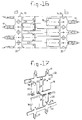
- Figure 16 shows third alternative shielding plates according to the invention;
- Figure 17 shows fourth alternative shielding plates according to the invention.
- In the Figures, the same reference numerals always refer to the same components. Figures 1a, b and c show a
connector 1 provided with femaleterminal connections 10; this connector is referred to below as "socket connector". The femaleterminal connections 10 clamp roundmale terminal pins 4 of theconnector 2 which mates therewith and which will be referred to below as "plug connector". In this connection, it is pointed out that, in the figures attached hereto, theplug connector 1 is always provided with two parallel rows ofmale terminal pins 4, but that it is always possible to replace one row thereof by a row of femaleterminal connections 10. The same applies, but in that case conversely, to the rows of female terminal connections in thesocket connector 1. It is possible, furthermore, to accommodate more than two rows of terminal connections in both the plug connector and the socket connector, with a shielding member between all the rows or between some of the rows. - Every female
terminal connection 10 leads, via feed-through 3 (or 11) to aprinted circuit board 7 for electrical connection to other circuit elements (not shown). Everyfemale terminal connection 10 has one feed-through 3 or 11: if, viewed in the longitudinal direction (Figure 1b), a particularterminal connection 10 has a feed-through 3, then theadjacent terminal connection 10 has a feed-through 11 which, viewed in cross section, is closer to the centre of the connector (Figure 1c) than the feed-through 3. The femaleterminal connections 10 are rigidly accommodated in aplastic housing 6. The end consists of two sprung lips which are able to clamp rigidly around a maleterminal pin 4 of aplug connector 2 in order, in this way, to make a rigid electrically conducting contact. In the width of thesocket connector 2 there is room for two parallel rows of female terminal connections 10 (Figure 1c). - Every
male terminal pin 4 is led further via a feed-through circuit board 8 for electrical connection to other circuit elements (not shown). Themale terminal pins 4 are rigidly accommodated in aplastic housing 5. Theplastic housing 5 of theplug connector 2 comprises twowalls 13 which grip round thehousing 6 of thesocket connector 1. Just like the feed-throughs throughs plug connector 1. In the width of theplug connector 1, there is always sufficient room for two adjacently situated rows of male terminal pins 4 (Figure 2c). - If the
connectors circuit board 7 and the printedcircuit board 8 is preferably 9.6 mm. The thickness x2 of the printedcircuit board - Figures 2a, b and c
show socket connector 1 and plugconnector 2 which grip into one another and which are both provided, according to the invention, with a shieldingplate socket connector 1 and theplug connector 2 are rigidly pushed against one another, the shieldingplates plate 14 leads via a feed-through 16 through the printedcircuit board 7, while the shieldingplate 15 is lead via a feed-through 17 through printedcircuit board 8. Via the feed-through 16 or 17 the shieldingplate - The spacing x3 between the printed
circuit boards circuit boards - Figure 3 shows Figure 2b enlarged. Here the construction of a preferred embodiment of the shielding
plate plate 15 comprises anelongated support 22. On one side of thesupport 22 there extend alternatelydifferent contact elements thin neck support 22. Thenecks contact elements support 22 in a direction perpendicular to the plane of the drawings of Figure 3. Thecontact element 18 is completely closed, whereas thecontact element 19 is provided with twolips lips dimples dimples closed contact element 18, situated opposite theopen contact element 19, of aplug counter connector 1 mating with theplug connector 2. This will be explained in still greater detail by reference to Figure 4. At the other side of thesupport 22 are the feed-throughs 17 which lead to the printedcircuit board 8. - The
contact elements contact elements necks small projections 44, against which the contact elements rest, are accommodated betweenadjacent contact elements socket connector 1, in place of thesmall projections 44 between some adjacent andcontact elements elongated projections 43, which fulfil the same function as thesmall projections 44 mentioned above can be accommodated in the wall of the housing. Both thesmall projections 44 and theprojections 43 also have a second function; they also rest against thesupport 22 of the shieldingplate 14 and thereby prevent the shielding plate from being able to move within the housing when the feed-throughs 16 of the shielding plate are pushed into openings, intended therefore, in the printedcircuit board 7. Theprojections 43 project outwards to such an extent inside thesocket connector 1 that they rest precisely against asmall projection 44 between twoadjacent contact elements plug connector 2 when thesocket connector 1 is connected to theplug connector 2. With the same object, theplug connector 2 may also contain someelongated projection 43 of this type. These latter are not shown in the Figure but are not, of course, situated opposite theprojections 43 in the housing of thesocket connector 1. - All the
open contact elements 19 may be provided with a notch 45 in the portion connecting the twolips - The shielding
plate 14 accommodated in thesocket connector 1 is identical to the shieldingplate 15 of theplug connector 2. The shieldingplates socket connector 1 or plugconnector 2, respectively, in such a way that aclosed contact element 18 always appears opposite anopen contact element 19. Variants of this are possible as will be explained below by reference to Figures 14 to 17 inclusive. - Essential to the invention is that both the
closed contact element 18 and theopen contact element 19 are constructed so as to spring with respect to thesupport 22. As a result, it is possible to make an electromagnetic screen between two rows of electrical connections, which screen has a maximum thickness of approximately twice the thickness of the plate material used for thescreen plate 14 of thesocket connector 1 is in contact with the shieldingplate 15 of theplug connector 2. The situation shown is that in which anopen contact element 19 of the shieldingplate 14 is in contact with aclosed contact element 18 of the shieldingplate 15. The small dimple 23 (24) ensures, under these circumstances, the desired mechanical contact stress between the two shieldingplates closed contact element 18 and the end of theopen contact element 19 are to some extent bent. Both theopen cbntact element 19 and theclosed contact 18 are bent aside to some extent as a consequence of the spring action. In the situation of Figure 4, theopen contact element 19 can give way somewhat further because the end thereof is situated in a funnel-shapedopening 25 provided in theplastic housing 6. Next to theopen contact element 19 is a closed contact element 18 (not shown) in thesocket connector 1, which closedcontact element 18 can bend aside somewhat further in its own funnel-shapedopening 25 than theopen contact element 19, mating therewith, of theplug connector 2. The total thickness which the plate-type shielding requires at the position of the contact between an open and a closed contact element is twice the thickness of the plate material used for the contact elements (preferably, 0.15 mm thick) plus twice the space which is needed for a bent end of each of the shieldingplates - Figures 5 to 8 inclusive show an individual
male plug connector 2 according to the invention in various views. Figure 5 shows a plan view of aplug connector 2. Theconnector 2 contains two rows of 21 male terminal pins 4. This number is only an example. Between the two rows there is a shielding plate of alternately closed andopen contact elements contact elements support 22 is cut through between two adjacent contact elements and the shielding consists of electrically separated sections each having their own voltage. Figure 5 shows four pairs of open andclosed contact elements plastic housing 5, thewall 13 has anopening 28 for mating with aprojection 29 of thesocket connector 1, while theother lip 13 has at itsends openings projections - Figure 6 shows a
separate plug connector 2 in cross section, the reference numerals being the same as in Figure 4. Figure 6 also reveals another characteristic of the present invention. Thesupport 22 of the shielding plate is situated in an opening 35 of thehousing 5. Because the support is provided withprotuberances 36, 37 and 38, the shielding cannot, however, easily be moved to and fro through the opening 35 of thehousing 5. On the other hand, by making use of theprotuberances 36, 37, 38, the openings 35 can be wider than the thickness of the plate material used for the shielding. As a result, prior to mounting the shielding in the opening 35, the end of thecontact element - Figure 7 shows a side view of the
plug connector 2 in which some preferred dimensions are included. The height x5 of the connector is preferably 7.4 mm, the height x6 to which the terminal pins project 2.5 mm, the height x7 of the base of thehousing 5 3.4 mm, the spacing x8 between the feed-through 17 of the shielding and the closest feed-through 12 of aterminal pin 4 in lateral projection 0.75 mm, the spacing x9 between two adjacent feed-throughs terminal pins 4 in lateral projection 1.0 mm, the thickness x10 of a terminal pin 0.4 mm, and the width x11 of the housing 4.5 mm. Of course, other dimensions are possible within the scope of the invention. - Figure 8 shows a cutaway longitudinal view of a
separate plug connector 2 according to the invention. After Figure 4, this figure does not require a separate explanation. - Figure 9 shows a plan view of a socket connector according to the invention. Two rows, each of 21
female terminal connections 10, are shown, which rows are separated by a shielding plate provided with four pairs of alternatingcontact elements projections openings female terminal connection 10 is able to mate with a maleterminal pin 4 of a plug connector. The closed andopen contact elements open contact element 19 always ends up opposite aclosed contact element 18, after which they come into contact with one another in a sliding manner and both are also bent to some extent in a sprung manner, as explained above. - Figure 9 shows some dimensions which, of course, also apply to the corresponding dimensions of the plug connector of Figure 5.
The width x12 of thesocket connector 1 is 3.5 mm, the spacing x13 between the shielding plate and the centres of thefemale terminal connections 10 1.0 mm, the spacing x14 between the centreline of the two rows of femaleterminal connections 10 2.0 mm, the total length x19 of thesocket connector 1 21.5 mm, the length x16 of theprojections projection 29 at the edge 10.75 mm, and the spacing x18 between two adjacent female terminal connections 1.0 mm. - Figure 10 shows a socket connector according to the invention in cross section. The funnel-shaped
opening 25 can be clearly seen and is intended for the bending-aside of the contact element 19 (or 18) if thesocket connector 1 is pushed into aplug connector 2 and the contact element 19 (or 18) comes into sliding contact with an oppositely situated contact element 18 (or 19) of the shieldingplate 15 of theplug connector 2. The shieldingplate 14 is led through anopening 39 of thehousing 6 in the same way as the shieldingplate 15 in Figure 6 after the end of the contact element 19 (or 18) has been bent. Theopening 39 is wider than the thickness of the plate material used for the shielding plate.Protuberances protuberances 36, 37 and 38 in Figure 6. The completely finished shieldingplate 14 is pushed from left to right through theopening 39 of thehousing 6 in the plane of the drawing in Figure 10. In other respects, Figure 10 requires no further explanation after Figure 4. - Figure 11 shows a side view of a
socket connector 1. The width x12 of the socket connector (cf. Figure 9) is 3.5 mm, while the width, inclusive of theprojections projection - Figure 12 shows a separate,
cutaway socket connector 1 in the longitudinal direction. The reference numerals are identical to those which have also been used in Figure 4, so that Figure 12 requires no separate explanation. - Figures 13a to d inclusive show separate strip-
type shieldings plates support 22 which has on its one side feed-throughs 17 for feeding through a printed circuit board. Provided at its other side are alternatelyclosed contact elements 18 andopen contact elements 19 which are bent to some extent at their end (Figure 13b and d). The ends of the open contact elements consist of twolips small dimple small notch 34 in the opening of theopen contact element 19 so that theopen contact element 19 is satisfactorily held in the correct position. - Figure 13c shows some dimensions for explaining the shielding plate according to the invention. The centre-to-centre spacing x24 between two
adjacent contact elements throughs 17 may also be 2.5 mm, but may be chosen independently of the spacing x24. The spacing x24 can also be freely chosen with respect to the spacing between adjacentterminal pins 4 or adjacentterminal connections 10. The centre-to-centre spacing x26 between thenecks adjacent contact elements adjacent contact elements - Figures 13b and d once again show clearly the
protuberances support 22 of a shielding plate which mate with an opening 39 (or 35) of the connector in which the shielding plate is positioned. - Figures 14a and b show a first variant of the shielding
plates plate contact elements 18 of Figure 14b are identical to those of Figure 13, while the contact elements 18' of Figure 14a are provided with small dimples 23', 24' which have the same function as thesmall dimples lips open contact element 19. The shieldingplates identical shielding plates one shielding plate contact elements 18, for example provided in aplug connector 2, is positioned opposite a shieldingplate socket connector 1 in such a way that thecontact elements 18 and 18' end up precisely opposite one another. Of course, it is also possible that all theplug connectors 2 are provided with shieldingplates socket connectors 1 with shieldingplates contact elements 18. - It is also possible to make one type of shielding
plates open contact elements 19 and one type of shieldingplates contact elements 18, as is explained in Figures 15a and b. Thesmall dimples lips closed contact elements 18. In the embodiment of Figures 15a and b, the shieldingplates open contact element 19 always appears precisely opposite aclosed contact element 18 one connects a plug connector to a socket connector. - In all the embodiments shown hitherto, there is always a narrow slit between
adjacent contact elements 18/19, 18/18, 18'/18' and 19/19 which slit continues to exist if a plug connector and a socket connector are pushed onto one another. Electromagnetic interference can still leak through the slit. This shortcoming can be remedied with the embodiment of Figures 16a and b. The embodiment of Figures 16a and b makes use of the same two shieldingplates plate plate contact elements 18 in the connector mating therewith (socket connector or plug connector) that if the two connectors are connected to one another, thecontact elements 18 and 18', respectively, completely close off the slit between oppositely situatedcontact elements 18' and 18, respectively. - The ends of the
contact elements shielding plates contact elements 18, 18' and/or 19 of a shielding plate are bent aside to the same side and the entire shielding plate is therefore under mechanical stress towards one side. If this is a drawback, it can be remedied by bendingadjacent contact elements adjacent contact elements closed contact elements 18. Such a construction is, however, also possible for the shielding plates of Figures 14 and 15 (not for those of Figure 16). The construction of Figure 17 eliminates, at least virtually, a mechanical stress on the entire shielding plate. - To increase the electrical conductivity, all the faces of the
contact elements mating contact elements - The invention is not limited to the exemplary embodiments described above. Any limitations ensue only from the attached claims. In the figures, for example, there are two parallel rows of
terminal pins 4, or parallel rows ofterminal connections 10, but in principle, a larger number of parallel rows is possible, with shieldings between each of the rows.
Claims (22)
- Electrical connector assembly, comprising a plug connector (2) and a socket connector (1) mating therewith, which plug connector and socket connector can be pushed into one another, which plug connector is provided with at least two rows of terminal connections (4) which are accommodated in a first plastic housing and at least one row of which consists of male terminal pins, and which socket connector is provided with at least two rows of terminal connections (10) which are accommodated in a second plastic housing and at least one row of which consists of female terminal connections, one male terminal pin (4) always being in electrically conducting contact with a female terminal connection (10) when plug connector and socket connector are pushed into one another, the plug connector (2) being provided with at least one electrically conducting first shielding member (15) arranged between said rows of terminal connections in the plug connector and being rigidly accommodated in the first housing, the socket connector (1) being provided with at least one conducting second shielding member (14) arranged between said rows of terminal connections in the socket connector and being rigidly accommodated in a second housing and comprising at least one resilient contact element, which first shielding member (15) and second shielding member (14) make electrically conducting contact with one another when the plug connector (2) and the socket connector (1) have been pushed into one another, characterized in that each said contact element of each said first shielding member (15) within the plug connector (2) is a resilient, flat contact element and in that each said contact element of the second shielding member (14) within the socket connector (1) is a resilient, flat contact element, in such a way that when the socket connecter (1) and the plug connecter (2) are connected to each other each contact element of the first shielding member (15) is slid along at least one contact element of the second shielding member (14).
- Electrical connector assembly according to Claim 1, wherein the first shielding member (15) is provided with an elongated support (22) to support each resilient contact element wherein each contact element is connected to the support (22) via a narrow neck (26, 27) providing the resilient action.
- Electrical connector assembly according to Claim 1 or 2, wherein the second shielding member (14) is provided with an elongated support (22) to support each resilient contact element wherein each contact element is connected to the support (22) via a narrow neck (26, 27) providing the resilient action.
- Electrical connector assembly according to Claim 1, 2 or 3, wherein the first shielding member (15) comprises several contact elements which are arranged alongside one another and consist of alternately closed contact elements (18) and open contact elements (19), the latter being provided with at least two lips (20, 21).
- Electrical connector assembly according to Claim 1, 2, 3 or 4, wherein the second shielding member (14) comprises several contact elements which are arranged alongside one another and consist of alternately closed contact elements (18) and open contact elements (19), the latter being provided with at least two lips (20, 21).
- Electrical connector assembly according to Claim 4 or 5, wherein a small dimple (23, 24) is provided on the ends of the lips (20, 21).
- Electrical connector assembly according to one of the preceding claims, wherein, when the plug connector (2) and the socket connector (1) are connected to one another, closed contact elements (18) are always situated opposite open contact elements (19).
- Electrical connector assembly according to Claim 1, 2 or 3, wherein the first shielding member (15) comprises several closed contact elements (18) situated alongside one another.
- Electrical connector assembly according to Claim 1, 2, 3 or 8, wherein the second shielding member (14) comprises several closed contact elements (18') situated alongside one another.
- Electrical connector assembly according to Claim 8 or 9, wherein the closed contact elements (18) of the first shielding member (15) are provided with small dimples (23', 24') at their end.
- Electrical connector assembly according to Claim 8 or 9, wherein the closed contact elements (18') of the second shielding member (14) are provided with small dimples (23', 24') at their end.
- Electrical connector assembly according to Claim 1, 2 or 3, wherein the first shielding member (15) comprises several closed contact elements (18) situated alongside one another and the second shielding member (14) comprises several open contact elements (19) situated alongside one another, and when the plug connector (2) and the socket connector (1) are connected to one another, each closed contact element (18) is situated opposite an open contact element (19).
- Electrical connector assembly according to Claim 1, 2 or 3, wherein the second shielding member (14) comprises several closed contact elements (18) situated alongside one another and the first shielding member (15) comprises several open contact elements (19) situated alongside on another, and when the plug connector (2) and the socket connector (1) are connected to one another, each closed contact element (18) is situated opposite an open contact element (19).
- Electrical connector assembly according to Claim 1, 2 or 3, wherein the second shielding member (14) comprises several closed contact elements (18') situated alongside one another and the first shielding member (15) comprises several closed contact elements (18) situated alongside one another, and when the plug connector (2) and the socket connector (1) are connected to one another, the closed contact elements (18') of the second shielding member (14) close off the opening between adjacent, oppositely situated closed contact elements (18) of the first shielding member (15) and the closed contact elements (18) of the first shielding member (15) close off the opening between adjacent, oppositely situated closed contact elements (18') of the second shielding member (14).
- Electrical connector assembly according to one of the preceding claims, wherein the ends of the contact elements of the second shielding member (14) are to some extent bent, and wherein the ends of the contact elements of the first shielding contact member (15) are also bent to some extent.
- Electrical connector assembly according to Claim 15, wherein the ends of adjacent contact elements of both the first (15) and the second (14) shielding member are to some extent bent, turn and turn about, to an oppositely facing side as seen in the connected state of the socket connector (1) and the plug connector (2).
- Electrical connector assembly according to one of the preceding claims, wherein projections (43, 44) situated between adjacent contact elements in the housing (5, 6) are provided against which the contact elements rest in the longitudinal direction of the connector (1, 2).
- Electrical connector assembly according to one of the preceding claims, wherein the first shielding member (15) is made of conducting plate material approximately 0.15 mm thick.
- Electrical connector assembly according to one of the preceding claims, wherein the second shielding member (14) is made of conducting plate material approximately 0.15 mm thick.
- Electrical connector assembly according to one of the preceding claims, wherein the open contact element (19) is provided with a notch (45) in a section which connects the two lips (20, 21) to one another, which notch (45) mates with a rib (46) provided on the wall of the respective housing (5, 6).
- Plug connector (2) of a connector assembly according to any of the preceding claims, provided with at least two rows of terminal connections (4) which are accommodated in a first plastic housing, at least one row of which consisting of male terminal pins, and at least one electrically conducting first shielding member (15) arranged between said rows of terminal connections in the plug connector and being rigidly accommodated in the first housing, characterized in that each said contact element of each said first shielding member (15) within the plug connector (2) is a resilient, flat contact element.
- Socket connector (1) of a connector assembly according to any of the claims 1 to 20 provided with at least two rows of terminal connections (10) which are accommodated in a second plastic housing, at least one row of which consisting of female terminal connections, and at least one conducting shielding member (14) arranged between said rows of terminal connections in the socket connector and being rigidly accommodated in a second housing and comprising at least one resilient contact element, characterized in that each said contact element of each said second shielding member (14) within the socket connector (1) is a resilient, flat contact element.
Applications Claiming Priority (3)
| Application Number | Priority Date | Filing Date | Title |
|---|---|---|---|
| NL9200119A NL9200119A (en) | 1992-01-22 | 1992-01-22 | CONNECTOR WITH PLATE-SHAPED INTERNAL SHIELD. |
| NL9200119 | 1992-01-22 | ||
| PCT/NL1993/000022 WO1993015533A1 (en) | 1992-01-22 | 1993-01-22 | Connector having plate-type internal shielding |
Publications (2)
| Publication Number | Publication Date |
|---|---|
| EP0623249A1 EP0623249A1 (en) | 1994-11-09 |
| EP0623249B1 true EP0623249B1 (en) | 1996-06-12 |
Family
ID=19860338
Family Applications (1)
| Application Number | Title | Priority Date | Filing Date |
|---|---|---|---|
| EP93904394A Expired - Lifetime EP0623249B1 (en) | 1992-01-22 | 1993-01-22 | Connector having plate-type internal shielding |
Country Status (9)
| Country | Link |
|---|---|
| US (1) | US5611700A (en) |
| EP (1) | EP0623249B1 (en) |
| JP (1) | JP3251586B2 (en) |
| KR (1) | KR950700619A (en) |
| DE (1) | DE69303158T2 (en) |
| HK (1) | HK162196A (en) |
| NL (1) | NL9200119A (en) |
| SG (1) | SG44712A1 (en) |
| WO (1) | WO1993015533A1 (en) |
Families Citing this family (9)
| Publication number | Priority date | Publication date | Assignee | Title |
|---|---|---|---|---|
| USD418111S (en) * | 1996-11-27 | 1999-12-28 | Thomas & Betts International, Inc. | Connector |
| DE19820144C1 (en) * | 1998-05-06 | 2000-03-02 | Harting Kgaa | Electrical connector |
| US6530790B1 (en) | 1998-11-24 | 2003-03-11 | Teradyne, Inc. | Electrical connector |
| DE19907635C1 (en) | 1999-02-23 | 2000-09-07 | Harting Kgaa | Shielded electrical connector |
| JP2002280124A (en) * | 2001-03-19 | 2002-09-27 | Jst Mfg Co Ltd | Electrical connector |
| US7489219B2 (en) * | 2003-07-16 | 2009-02-10 | Marvell World Trade Ltd. | Power inductor with reduced DC current saturation |
| US7307502B2 (en) * | 2003-07-16 | 2007-12-11 | Marvell World Trade Ltd. | Power inductor with reduced DC current saturation |
| US7023313B2 (en) * | 2003-07-16 | 2006-04-04 | Marvell World Trade Ltd. | Power inductor with reduced DC current saturation |
| US8324872B2 (en) * | 2004-03-26 | 2012-12-04 | Marvell World Trade, Ltd. | Voltage regulator with coupled inductors having high coefficient of coupling |
Family Cites Families (8)
| Publication number | Priority date | Publication date | Assignee | Title |
|---|---|---|---|---|
| US3660803A (en) * | 1969-10-08 | 1972-05-02 | Ncr Co | Electrical connectors |
| US4655518A (en) * | 1984-08-17 | 1987-04-07 | Teradyne, Inc. | Backplane connector |
| US5004427A (en) * | 1986-06-19 | 1991-04-02 | Labinal Components And Systems, Inc. | Electrical connectors |
| US5169324A (en) * | 1986-11-18 | 1992-12-08 | Lemke Timothy A | Plug terminator having a grounding member |
| US4762500A (en) * | 1986-12-04 | 1988-08-09 | Amp Incorporated | Impedance matched electrical connector |
| DE8713091U1 (en) * | 1987-09-29 | 1987-12-23 | Siemens AG, 1000 Berlin und 8000 München | Multi-pole connector with special contacts |
| EP0455367B1 (en) * | 1990-05-04 | 1996-06-19 | The Whitaker Corporation | Right angle impedance matched electrical connector |
| US5046960A (en) | 1990-12-20 | 1991-09-10 | Amp Incorporated | High density connector system |
-
1992
- 1992-01-22 NL NL9200119A patent/NL9200119A/en not_active Application Discontinuation
-
1993
- 1993-01-22 SG SG1996006184A patent/SG44712A1/en unknown
- 1993-01-22 DE DE69303158T patent/DE69303158T2/en not_active Expired - Fee Related
- 1993-01-22 EP EP93904394A patent/EP0623249B1/en not_active Expired - Lifetime
- 1993-01-22 WO PCT/NL1993/000022 patent/WO1993015533A1/en not_active Ceased
- 1993-01-22 JP JP51310693A patent/JP3251586B2/en not_active Expired - Fee Related
- 1993-01-22 US US08/256,753 patent/US5611700A/en not_active Expired - Lifetime
-
1994
- 1994-07-22 KR KR1019940702527A patent/KR950700619A/en not_active Withdrawn
-
1996
- 1996-08-29 HK HK162196A patent/HK162196A/en not_active IP Right Cessation
Also Published As
| Publication number | Publication date |
|---|---|
| NL9200119A (en) | 1993-08-16 |
| WO1993015533A1 (en) | 1993-08-05 |
| HK162196A (en) | 1996-09-06 |
| JPH07506692A (en) | 1995-07-20 |
| DE69303158T2 (en) | 1997-01-23 |
| JP3251586B2 (en) | 2002-01-28 |
| EP0623249A1 (en) | 1994-11-09 |
| SG44712A1 (en) | 1997-12-19 |
| US5611700A (en) | 1997-03-18 |
| DE69303158D1 (en) | 1996-07-18 |
| KR950700619A (en) | 1995-01-16 |
Similar Documents
| Publication | Publication Date | Title |
|---|---|---|
| EP1465298B1 (en) | Controlled impedance cable connector | |
| US5620340A (en) | Connector with improved shielding | |
| JP3016164B2 (en) | Movable connector | |
| US7037117B2 (en) | Electrical connector with regulation means | |
| EP0284245B1 (en) | High-density, modular, electrical connector | |
| US6645003B2 (en) | Joint connector | |
| KR940011264B1 (en) | Connector with grounding structure | |
| EP0403370A1 (en) | Multi-row box connector | |
| EP1485971B1 (en) | Method of assembling an electrical connector | |
| NL9202302A (en) | Koaxial interconnection system. | |
| EP1147577B1 (en) | Low profile electrical connector | |
| US6524117B1 (en) | Electric connecting apparatus for electrically connecting two electric components | |
| US4201432A (en) | Electric connectors | |
| US7479019B2 (en) | Intelligent connector assembly for use in medical device cables | |
| EP0503578B1 (en) | Shunted electrical connector | |
| US5611700A (en) | Connector having plate-type internal shielding | |
| GB2147466A (en) | Mounting block for interconnecting connectors to a printed circuit board | |
| EP0677215B1 (en) | A connector with improved shielding | |
| NZ299112A (en) | Terminal block with insulation displacement contacts and shield plates in transverse walls between chambers | |
| US4734045A (en) | High density connector | |
| DE69623669T2 (en) | Electrical connector with multi-position filter adapter | |
| US4804336A (en) | Double fifty plug-socket connector | |
| JPS58135586A (en) | Electric contact and its application | |
| CN1113436C (en) | Mechanical connecting device | |
| JPH0241857Y2 (en) |
Legal Events
| Date | Code | Title | Description |
|---|---|---|---|
| PUAI | Public reference made under article 153(3) epc to a published international application that has entered the european phase |
Free format text: ORIGINAL CODE: 0009012 |
|
| 17P | Request for examination filed |
Effective date: 19940701 |
|
| AK | Designated contracting states |
Kind code of ref document: A1 Designated state(s): DE FR GB |
|
| 17Q | First examination report despatched |
Effective date: 19950131 |
|
| GRAH | Despatch of communication of intention to grant a patent |
Free format text: ORIGINAL CODE: EPIDOS IGRA |
|
| GRAH | Despatch of communication of intention to grant a patent |
Free format text: ORIGINAL CODE: EPIDOS IGRA |
|
| RAP1 | Party data changed (applicant data changed or rights of an application transferred) |
Owner name: BERG ELECTRONICS MANUFACTURING B.V. |
|
| GRAA | (expected) grant |
Free format text: ORIGINAL CODE: 0009210 |
|
| AK | Designated contracting states |
Kind code of ref document: B1 Designated state(s): DE FR GB |
|
| REF | Corresponds to: |
Ref document number: 69303158 Country of ref document: DE Date of ref document: 19960718 |
|
| ET | Fr: translation filed | ||
| REG | Reference to a national code |
Ref country code: GB Ref legal event code: 732E |
|
| RAP2 | Party data changed (patent owner data changed or rights of a patent transferred) |
Owner name: BERG ELECTRONICS MANUFACTURING B.V. Owner name: CONNECTOR SYSTEMS TECHNOLOGY N.V. |
|
| PLBE | No opposition filed within time limit |
Free format text: ORIGINAL CODE: 0009261 |
|
| STAA | Information on the status of an ep patent application or granted ep patent |
Free format text: STATUS: NO OPPOSITION FILED WITHIN TIME LIMIT |
|
| 26N | No opposition filed | ||
| REG | Reference to a national code |
Ref country code: GB Ref legal event code: 732E |
|
| REG | Reference to a national code |
Ref country code: FR Ref legal event code: TP |
|
| REG | Reference to a national code |
Ref country code: GB Ref legal event code: IF02 |
|
| PGFP | Annual fee paid to national office [announced via postgrant information from national office to epo] |
Ref country code: GB Payment date: 20041210 Year of fee payment: 13 |
|
| PGFP | Annual fee paid to national office [announced via postgrant information from national office to epo] |
Ref country code: FR Payment date: 20050105 Year of fee payment: 13 |
|
| PG25 | Lapsed in a contracting state [announced via postgrant information from national office to epo] |
Ref country code: GB Free format text: LAPSE BECAUSE OF NON-PAYMENT OF DUE FEES Effective date: 20060122 |
|
| PG25 | Lapsed in a contracting state [announced via postgrant information from national office to epo] |
Ref country code: FR Free format text: LAPSE BECAUSE OF NON-PAYMENT OF DUE FEES Effective date: 20060131 |
|
| GBPC | Gb: european patent ceased through non-payment of renewal fee |
Effective date: 20060122 |
|
| REG | Reference to a national code |
Ref country code: FR Ref legal event code: ST Effective date: 20060929 |
|
| PGFP | Annual fee paid to national office [announced via postgrant information from national office to epo] |
Ref country code: DE Payment date: 20080131 Year of fee payment: 16 |
|
| PG25 | Lapsed in a contracting state [announced via postgrant information from national office to epo] |
Ref country code: DE Free format text: LAPSE BECAUSE OF NON-PAYMENT OF DUE FEES Effective date: 20090801 |