EP0622624B1 - A method for observing film thickness and/or refractive index - Google Patents
A method for observing film thickness and/or refractive index Download PDFInfo
- Publication number
- EP0622624B1 EP0622624B1 EP94302911A EP94302911A EP0622624B1 EP 0622624 B1 EP0622624 B1 EP 0622624B1 EP 94302911 A EP94302911 A EP 94302911A EP 94302911 A EP94302911 A EP 94302911A EP 0622624 B1 EP0622624 B1 EP 0622624B1
- Authority
- EP
- European Patent Office
- Prior art keywords
- refractive index
- film thickness
- light beams
- reflected
- colour
- Prior art date
- Legal status (The legal status is an assumption and is not a legal conclusion. Google has not performed a legal analysis and makes no representation as to the accuracy of the status listed.)
- Expired - Lifetime
Links
Images


Classifications
-
- G—PHYSICS
- G01—MEASURING; TESTING
- G01B—MEASURING LENGTH, THICKNESS OR SIMILAR LINEAR DIMENSIONS; MEASURING ANGLES; MEASURING AREAS; MEASURING IRREGULARITIES OF SURFACES OR CONTOURS
- G01B11/00—Measuring arrangements characterised by the use of optical techniques
- G01B11/02—Measuring arrangements characterised by the use of optical techniques for measuring length, width or thickness
- G01B11/06—Measuring arrangements characterised by the use of optical techniques for measuring length, width or thickness for measuring thickness ; e.g. of sheet material
- G01B11/0616—Measuring arrangements characterised by the use of optical techniques for measuring length, width or thickness for measuring thickness ; e.g. of sheet material of coating
- G01B11/0641—Measuring arrangements characterised by the use of optical techniques for measuring length, width or thickness for measuring thickness ; e.g. of sheet material of coating with measurement of polarization
-
- G—PHYSICS
- G01—MEASURING; TESTING
- G01N—INVESTIGATING OR ANALYSING MATERIALS BY DETERMINING THEIR CHEMICAL OR PHYSICAL PROPERTIES
- G01N21/00—Investigating or analysing materials by the use of optical means, i.e. using sub-millimetre waves, infrared, visible or ultraviolet light
- G01N21/17—Systems in which incident light is modified in accordance with the properties of the material investigated
- G01N21/21—Polarisation-affecting properties
-
- G—PHYSICS
- G01—MEASURING; TESTING
- G01N—INVESTIGATING OR ANALYSING MATERIALS BY DETERMINING THEIR CHEMICAL OR PHYSICAL PROPERTIES
- G01N21/00—Investigating or analysing materials by the use of optical means, i.e. using sub-millimetre waves, infrared, visible or ultraviolet light
- G01N21/17—Systems in which incident light is modified in accordance with the properties of the material investigated
- G01N21/41—Refractivity; Phase-affecting properties, e.g. optical path length
- G01N2021/4126—Index of thin films
-
- G—PHYSICS
- G01—MEASURING; TESTING
- G01N—INVESTIGATING OR ANALYSING MATERIALS BY DETERMINING THEIR CHEMICAL OR PHYSICAL PROPERTIES
- G01N21/00—Investigating or analysing materials by the use of optical means, i.e. using sub-millimetre waves, infrared, visible or ultraviolet light
- G01N21/84—Systems specially adapted for particular applications
- G01N21/8422—Investigating thin films, e.g. matrix isolation method
Definitions
- the present invention relates to a method for observing film thickness and/or refractive index by colour difference. More particularly, the present invention relates to a method for observing film thickness and/or refractive index by colour difference which is useful in the development and evaluation of new materials, and in the observation of the refractive index of a solid or liquid surface in various industrial areas including electronics, the refractive index of a thin film on the surface of a solid or a liquid, and changes in film thickness as well as two dimensional distributions of film thickness.
- SIMS Secondary ion mass spectrography
- the optical methods include the technique of measuring the intensity of transmitted and fluorescent light, but the most reliable way of measuring film thickness is to use an ellipsometer.
- ellipsometer Several types have been developed in recent years to allow for the dynamic measurement of two-dimensional distributions of film thickness and/or refractive index of a thin film on the surface of a material. These ellipsometers are used very often in various methods today.
- the ellipsometric method may be classified into two types, as follows:
- Method (1) inevitably involves mechanical vibration because the sample must be moved in the measurement.
- the method is not applied to the measurement of liquid surfaces. Further, it takes a long time to scan a sample because the motion of the sample is mechanical.
- Method (2) requires the acquisition of multiple digitized images of the intensity of reflected light beams. This involves a long time for completing a run. Further, dozens of images are required to derive a practical level of precision in the measurement of refractive index, and this in turn necessitates the use of a huge memory capacity or an external memory. Similar complex measuring steps must be followed, and thus similar time usage is necessary, for deriving the two-dimensional distribution for just a single refractive index.
- the present invention was developed in consideration of the above circumstances and aims to solve the problems in the conventional methods by providing a novel method for observing film thickness and/or refractive index; for confirming two-dimensional distribution of refractive index and film thickness and their dynamic change with ease and visually; for observing surface phenomena on a real time basis; and for measuring a liquid surface.
- the present invention provides a method for observing film thickness and/or refractive index, wherein light from a white light source is irradiated onto the surface of a solid or liquid, and the film thickness or refractive index is determined on the basis of the partial extinction of the reflected light, the colour of the reflected light being used as an indication of said film thickness and/or refractive index.
- the present invention further provides a method for observing film thickness and/or refractive index at enhanced sensitivity with an increased colour difference, wherein the reflected light is incident on the surface of the same solid or liquid again, repeating this re-incidence more than once.
- the basic feature of the present invention consists of the partial extinction and the colouring of reflected light beams as described above. This feature permits observation of the difference in film thickness and/or refractive index by colour difference.
- the extinction method is described below.
- Equation (5) indicates that the reflected light beams can be changed into linearly polarised light beams at any time simply by adjusting ⁇ 0 .
- Linearly polarized light beams can be extinguished by a polariser.
- ⁇ s and ⁇ s are a function of wavelength.
- equation (5) is satisfied for a given wavelength in a given incident light with respect to said wavelength, incident angle, film thickness, refractive index for said wavelength, and refractive index of the substrate for said wavelength, then, generally, equation (5) is not satisfied for any other wavelength, and the reflected light beams are linearly polarized only at said single wavelength. Accordingly, only one wavelength can be extinguished when using a polariser. This is called partial extinction.
- the partially extinct light beams are coloured in the complementary colour to the extinct colour.
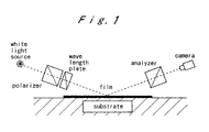
- Figure 1 shows an example of a system for partial extinction.
- the substrate surface to be observed is covered with a thin film of a certain refractive index distribution.
- a white light source is generally used for an ordinary extinction type ellipsometer.
- Reflected light beams pass through a detector (that is, polarizer).
- polarizer that is, polarizer
- the first axis (optical fast axis) of the wave plate is set in the 45 or 135 degree direction.
- the reflected light beams in this instance are tinted in a certain colour corresponding to a specific film thickness and refractive index because the light beams are partially extinct.
- An area whose refractive index is the same as the above is a place where similar partial extinction takes place, and is tinted in the came colour.
- Spectral intensity of the reflected light beams in this instance reaches the lowest level at the wavelength ( ⁇ 0 ) where partial extinction took place, as shown in Figure 3 for example.
- the light beams which are reflected from there are either not linearly polarized or are linearly polarised at a different wavelength, and thus are either not partially extinct or are partially extinct at these different wavelengths.
- the spectral intensity reaches the lowest level in these cases at different wavelengths (for example, ⁇ 1 ).
- the smallest wavelength is different, the colour is also different, with the result that one will see different colours depending on location. It is possible to shoot the reflected light beams with a camera.
- the ⁇ s in equation (5) doubles when the light reflected from the surface of the sample in the above method is reflected from a mirror and re-incident on the same surface. This means that the light beams are reflected from the same surface twice and are polarized two times larger than those reflected only once.
- the difference in polarization of other reflected light beams from other locations on the same sample having a different film thickness and/or refractive index also doubles. As a result, the colour difference increases. This suggests that a very small difference in film thickness and/or refractive index may possibly be identified by a colour difference.
- Figure 2 shows an example of a system by which the reflected light beams can be re-incidence on the same surface.
- the detecting device may be a spectroscope, in which case quantification is possible.
- a camera, colour CCD camera, spectroscope and other devices may also be used.
- specific correspondence between colour and film thickness is predetermined for a specific sample, then one can determine film thickness by observing colour with a camera or a colour CCD camera. In this case, of course, identification is impossible unless the colour difference due to different film thickness has at least a certain size. When this condition is satisfied, film thickness can be accurately determined by the colour observed under the spectroscope.
- FIGS. 1 and 2 show examples of systems for the present invention.
- light beams from a white light source are specifically polarized by a polarizer and a quarter wave plate and are incident on the surface of a sample.
- the condition of polarization varies and the light beams are reflected from the sample surface, and pass through a detector, finally reaching a camera.
- the system shown in figure 2 allows observation at an enhanced sensitivity.
- Light beams, which are incident on and reflected from the surface of a sample are further reflected from a reflector, and incident on the surface of the same sample again.
- the condition of polarization also varies here.
- the light beams are reflected from a half mirror at 90 degrees, and pass through a detector, finally reaching a camera.
- the reflectivity of the half mirror depends on polarization.
- the dependency should be as small as possible.
- the reflectivity of the half mirror to be used should not depend on wavelength excessively.
- the sample was a silicon wafer provided with an oxide film which was about 2 nm thick.
- a resist film was applied to the surface of the sample.
- the sample was immersed in a 10% HF solution for about 30 seconds, and then washed in pure water, and the resist film was removed with acetone, ready for observation.
- the area protected by the resist film was covered with the oxide film which retained its original thickness.
- the resultant surface had a profile in the depth direction.
- a halogen lamp was used as the light source, and prisms were used as the polarizer and detector.
- the angle of the polarizer and detector was so adjusted as to extinguish light of 550 nm wavelength using the system shown in figure 2.
- the result was shot with a camera.
- Figure 4 shows an example. One can read the word "ERATO".
- the area of residual oxide film was white and the surrounding area was blue.
- the A of the oxide film was 168 degrees and ⁇ was 11.8 degrees. Those for the surrounding area were 172 and 11.8 degrees, respectively. These differences are equivalent to approximately 1 nm as the difference of film thickness.
- the present invention makes it possible to discern film thickness and refractive index distribution by colour difference and observe surface phenomena on a real-time basis. It further enables more sensitive observation. Liquid surfaces can also be observed because it is not necessary to move samples in the observation.
Landscapes
- Physics & Mathematics (AREA)
- General Physics & Mathematics (AREA)
- Health & Medical Sciences (AREA)
- Life Sciences & Earth Sciences (AREA)
- Chemical & Material Sciences (AREA)
- Analytical Chemistry (AREA)
- Biochemistry (AREA)
- General Health & Medical Sciences (AREA)
- Immunology (AREA)
- Pathology (AREA)
- Length Measuring Devices By Optical Means (AREA)
- Investigating Or Analysing Materials By Optical Means (AREA)
Description
- The present invention relates to a method for observing film thickness and/or refractive index by colour difference. More particularly, the present invention relates to a method for observing film thickness and/or refractive index by colour difference which is useful in the development and evaluation of new materials, and in the observation of the refractive index of a solid or liquid surface in various industrial areas including electronics, the refractive index of a thin film on the surface of a solid or a liquid, and changes in film thickness as well as two dimensional distributions of film thickness.
- The study of the condition of a surface is very important in the development and evaluation of new materials, and in the electronics industry. In the production of silicon oxide film on a silicon wafer board, for example, two dimensional film thickness distribution for the silicon oxide film must be confirmed by surface analysis to a precision in the order of a nanometer.
- It is thus necessary to observe film thickness, and further, refractive index, of a solid or a liquid as a two dimensional distribution or a dynamic change.
- Conventional surface analysis methods, most of which derive from a scanning microscope, include Auger, ESCA, and EPMA, which are useful for local detection or identification of materials, and material analysis.
- Secondary ion mass spectrography (SIMS), which is one of the conventional methods, is used to measure material distribution in the depth direction.
- However, only the optical methods provide a way of evaluating film thickness and optical properties to a high degree of precision, whatever the materials may be.
- The optical methods include the technique of measuring the intensity of transmitted and fluorescent light, but the most reliable way of measuring film thickness is to use an ellipsometer.
- Several types of ellipsometer have been developed in recent years to allow for the dynamic measurement of two-dimensional distributions of film thickness and/or refractive index of a thin film on the surface of a material. These ellipsometers are used very often in various methods today. The ellipsometric method may be classified into two types, as follows:
- (1) A method to measure two-dimensional distribution by measuring the film thickness and refractive index of a sample using a light beam which is squeezed into a spot of the order of 10 µm in diameter, while moving the sample over a plane (M. Erman and J.B. Theeten, J. Appl. Phys., 60, 859 [1986]); and
- (2) A method to record multiple images of the intensity of reflected light beams on a detector using a CCD camera to calculate two-dimensional distributions of film thickness and refractive index of a thin film placed on a substrate (D. Beaglehole, Rev. Sci. Instrum., 59, 2557 [1988]).
-
- Method (1) inevitably involves mechanical vibration because the sample must be moved in the measurement. In addition, the method is not applied to the measurement of liquid surfaces. Further, it takes a long time to scan a sample because the motion of the sample is mechanical.
- Method (2) requires the acquisition of multiple digitized images of the intensity of reflected light beams. This involves a long time for completing a run. Further, dozens of images are required to derive a practical level of precision in the measurement of refractive index, and this in turn necessitates the use of a huge memory capacity or an external memory. Similar complex measuring steps must be followed, and thus similar time usage is necessary, for deriving the two-dimensional distribution for just a single refractive index.
- Further ellipsometer systems are shown in, for example, EP-A-0144115, EP-A-0019088, and JP-A-04294227.
- The present invention was developed in consideration of the above circumstances and aims to solve the problems in the conventional methods by providing a novel method for observing film thickness and/or refractive index; for confirming two-dimensional distribution of refractive index and film thickness and their dynamic change with ease and visually; for observing surface phenomena on a real time basis; and for measuring a liquid surface.
- To solve the above problems, the present invention provides a method for observing film thickness and/or refractive index, wherein light from a white light source is irradiated onto the surface of a solid or liquid, and the film thickness or refractive index is determined on the basis of the partial extinction of the reflected light, the colour of the reflected light being used as an indication of said film thickness and/or refractive index.
- The present invention further provides a method for observing film thickness and/or refractive index at enhanced sensitivity with an increased colour difference, wherein the reflected light is incident on the surface of the same solid or liquid again, repeating this re-incidence more than once.
- Embodiments of the present invention will now be described, by way of example only, with reference to the accompanying drawings, in which:
- Fig. 1 is a structural view of a system for partial extinction of reflected light beams according to a first embodiment of the present invention;
- Fig. 2 is a structural view of a system for partial extinction of reflected re-incident light beams according to a second embodiment of the present invention;
- Fig. 3 is a diagram illustrating the relation between the spectral intensity of reflected light beams partially extinguished and the spectral intensity of reflected light beams from an area with a different film thickness and refractive index; and
- Fig. 4 is a photograph from a working example of the present invention.
-
- The basic feature of the present invention consists of the partial extinction and the colouring of reflected light beams as described above. This feature permits observation of the difference in film thickness and/or refractive index by colour difference.
- The above feature permits:
- (1) the observation of film thickness and/or refractive index distribution by the difference in colour;
- (2) the real-time observation of surface phenomena; and
- (3) the possibility of the observation of a liquid surface because the sample need not be moved during measurement.
-
- Further, all of these observations can be performed to a high degree of sensitivity.
- The working of the present invention is described first with respect to the extinction method (the principle of the extinction type ellipsometer), followed by a description of partial extinction.
- The extinction method is described below. The condition of a polarized light beam is defined by the following formula:
- By using the following relations:we obtain:
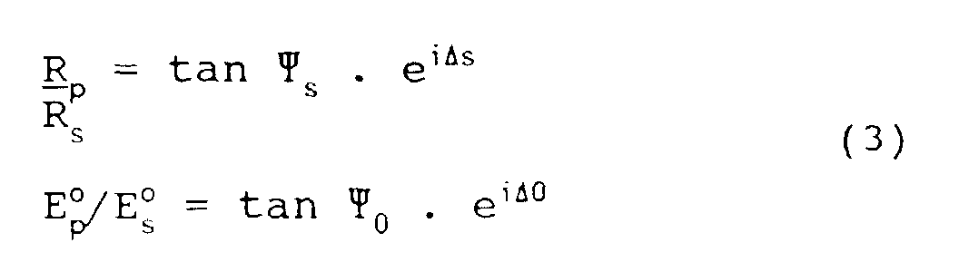
- Equation (5) indicates that the reflected light beams can be changed into linearly polarised light beams at any time simply by adjusting Δ0. Linearly polarized light beams can be extinguished by a polariser. Based on the direction of the electric field vector in this instance, Ψ to satisfy tan Ψ = tan Ψs.tan Ψ0 can be known. Since Δ0 and Ψ0 are known, Δs and Ψs can be known readily. Since film thickness and refractive index of the film are the only two unknowns, these can be known from Δs and Ψs. This is the principle of the extinction method in the ellipsometer.
- Partial extinction is described below.
- Assume the light source is white light. White light contains all light wavelengths at the same intensity. In this instance, generally, Δs and Ψs are a function of wavelength. When equation (5) is satisfied for a given wavelength in a given incident light with respect to said wavelength, incident angle, film thickness, refractive index for said wavelength, and refractive index of the substrate for said wavelength, then, generally, equation (5) is not satisfied for any other wavelength, and the reflected light beams are linearly polarized only at said single wavelength. Accordingly, only one wavelength can be extinguished when using a polariser. This is called partial extinction. The partially extinct light beams are coloured in the complementary colour to the extinct colour.
- Figure 1 shows an example of a system for partial extinction. The substrate surface to be observed is covered with a thin film of a certain refractive index distribution. A white light source is generally used for an ordinary extinction type ellipsometer. Reflected light beams pass through a detector (that is, polarizer). By properly adjusting the angle of the detector and also the angle of the polarizer on the incident side, partial extinction takes place on the surface of the substrate at a certain wavelength corresponding to the given thin film thickness and refractive index. The first axis (optical fast axis) of the wave plate is set in the 45 or 135 degree direction.
- The reflected light beams in this instance are tinted in a certain colour corresponding to a specific film thickness and refractive index because the light beams are partially extinct. An area whose refractive index is the same as the above is a place where similar partial extinction takes place, and is tinted in the came colour. Spectral intensity of the reflected light beams in this instance reaches the lowest level at the wavelength (λ0) where partial extinction took place, as shown in Figure 3 for example. At other locations having different refractive indices, the light beams which are reflected from there are either not linearly polarized or are linearly polarised at a different wavelength, and thus are either not partially extinct or are partially extinct at these different wavelengths. The spectral intensity reaches the lowest level in these cases at different wavelengths (for example, λ1). When the smallest wavelength is different, the colour is also different, with the result that one will see different colours depending on location. It is possible to shoot the reflected light beams with a camera.
- The Δs in equation (5) doubles when the light reflected from the surface of the sample in the above method is reflected from a mirror and re-incident on the same surface. This means that the light beams are reflected from the same surface twice and are polarized two times larger than those reflected only once. The difference in polarization of other reflected light beams from other locations on the same sample having a different film thickness and/or refractive index also doubles. As a result, the colour difference increases. This suggests that a very small difference in film thickness and/or refractive index may possibly be identified by a colour difference.
- When the reflected light beams are re-incident on the same surface more than twice, then more sensitive observation is possible. Of course, attenuation of the reflected light beams must be considered. Figure 2 shows an example of a system by which the reflected light beams can be re-incidence on the same surface.
- It goes without saying that various embodiments are possible for the present invention which is based on the above working principle. For example, in the present invention, the detecting device may be a spectroscope, in which case quantification is possible. A camera, colour CCD camera, spectroscope and other devices may also be used. When specific correspondence between colour and film thickness is predetermined for a specific sample, then one can determine film thickness by observing colour with a camera or a colour CCD camera. In this case, of course, identification is impossible unless the colour difference due to different film thickness has at least a certain size. When this condition is satisfied, film thickness can be accurately determined by the colour observed under the spectroscope.
- Working examples are shown below to further describe the present invention in detail.
- The attached Figures 1 and 2 show examples of systems for the present invention. In the present invention, as shown in Figure 1, light beams from a white light source are specifically polarized by a polarizer and a quarter wave plate and are incident on the surface of a sample. The condition of polarization varies and the light beams are reflected from the sample surface, and pass through a detector, finally reaching a camera. The system shown in figure 2 allows observation at an enhanced sensitivity. Light beams, which are incident on and reflected from the surface of a sample, are further reflected from a reflector, and incident on the surface of the same sample again. The condition of polarization also varies here. The light beams are reflected from a half mirror at 90 degrees, and pass through a detector, finally reaching a camera.
- It is important, in this instance, to keep in mind that the reflectivity of the half mirror depends on polarization. The dependency should be as small as possible. The reflectivity of the half mirror to be used should not depend on wavelength excessively.
- The difference of film thickness was actually observed on the surface of a silicon wafer substrate using the system shown in Figure 2 which is constructed in Working Example 1.
- The sample was a silicon wafer provided with an oxide film which was about 2 nm thick. A resist film was applied to the surface of the sample. The sample was immersed in a 10% HF solution for about 30 seconds, and then washed in pure water, and the resist film was removed with acetone, ready for observation. The area protected by the resist film was covered with the oxide film which retained its original thickness. The resultant surface had a profile in the depth direction.
- A halogen lamp was used as the light source, and prisms were used as the polarizer and detector. The angle of the polarizer and detector was so adjusted as to extinguish light of 550 nm wavelength using the system shown in figure 2. The result was shot with a camera. Figure 4 shows an example. One can read the word "ERATO".
- The area of residual oxide film was white and the surrounding area was blue. The A of the oxide film was 168 degrees and Ψ was 11.8 degrees. Those for the surrounding area were 172 and 11.8 degrees, respectively. These differences are equivalent to approximately 1 nm as the difference of film thickness.
- As described above in detail, the present invention makes it possible to discern film thickness and refractive index distribution by colour difference and observe surface phenomena on a real-time basis. It further enables more sensitive observation. Liquid surfaces can also be observed because it is not necessary to move samples in the observation.
Claims (3)
- A method of observing film thickness and/or refractive index, wherein light from a white light source is irradiated onto the surface of a solid or liquid, and the film thickness or refractive index is determined on the basis of the partial extinction of the reflected light, the colour of the reflected light being used as an indication of said film thickness and/or refractive index.
- The method of claim 1, wherein the light is reflected from the surface more than once.
- The method of claim 1 or 2, wherein the film thickness and/or refractive index distribution across the surface is determined on the basis of differences in the colour of the light reflected from the different thickness and/or different refractive index regions of the surface.
Applications Claiming Priority (6)
| Application Number | Priority Date | Filing Date | Title |
|---|---|---|---|
| JP5097794A JP2851987B2 (en) | 1993-04-23 | 1993-04-23 | Color difference observation method for film thickness and refractive index |
| JP97794/93 | 1993-04-23 | ||
| JP9779493 | 1993-04-23 | ||
| JP15224793 | 1993-06-23 | ||
| JP5152247A JP2790410B2 (en) | 1993-06-23 | 1993-06-23 | High sensitivity color difference observation method for film thickness and refractive index |
| JP152247/93 | 1993-06-23 |
Publications (2)
| Publication Number | Publication Date |
|---|---|
| EP0622624A1 EP0622624A1 (en) | 1994-11-02 |
| EP0622624B1 true EP0622624B1 (en) | 1999-12-01 |
Family
ID=26438938
Family Applications (1)
| Application Number | Title | Priority Date | Filing Date |
|---|---|---|---|
| EP94302911A Expired - Lifetime EP0622624B1 (en) | 1993-04-23 | 1994-04-25 | A method for observing film thickness and/or refractive index |
Country Status (3)
| Country | Link |
|---|---|
| US (1) | US5610392A (en) |
| EP (1) | EP0622624B1 (en) |
| DE (1) | DE69421844T2 (en) |
Families Citing this family (32)
| Publication number | Priority date | Publication date | Assignee | Title |
|---|---|---|---|---|
| US6278519B1 (en) | 1998-01-29 | 2001-08-21 | Therma-Wave, Inc. | Apparatus for analyzing multi-layer thin film stacks on semiconductors |
| US5798837A (en) | 1997-07-11 | 1998-08-25 | Therma-Wave, Inc. | Thin film optical measurement system and method with calibrating ellipsometer |
| US6483580B1 (en) | 1998-03-06 | 2002-11-19 | Kla-Tencor Technologies Corporation | Spectroscopic scatterometer system |
| US6236459B1 (en) | 1998-11-05 | 2001-05-22 | University Of Miami | Thin film measuring device and method |
| US6256097B1 (en) * | 1999-01-08 | 2001-07-03 | Rudolph Technologies, Inc. | Ellipsometer and ellipsometry method |
| JP2003508772A (en) * | 1999-07-27 | 2003-03-04 | コロラド・スクール・オブ・マインズ | Parallel detection spectroscopic ellipsometer / polarimeter |
| US6812047B1 (en) * | 2000-03-08 | 2004-11-02 | Boxer Cross, Inc. | Evaluating a geometric or material property of a multilayered structure |
| US6781692B1 (en) * | 2000-08-28 | 2004-08-24 | Therma-Wave, Inc. | Method of monitoring the fabrication of thin film layers forming a DWDM filter |
| DE10045210A1 (en) * | 2000-09-13 | 2002-05-02 | Infineon Technologies Ag | Method and device for detecting layers deposited on a wafer |
| WO2003054475A2 (en) * | 2001-12-19 | 2003-07-03 | Kla-Tencor Technologies Corporation | Parametric profiling using optical spectroscopic systems |
| JP2004219261A (en) * | 2003-01-15 | 2004-08-05 | Fuji Photo Film Co Ltd | Thin film analysis method |
| US7515253B2 (en) | 2005-01-12 | 2009-04-07 | Kla-Tencor Technologies Corporation | System for measuring a sample with a layer containing a periodic diffracting structure |
| KR100913484B1 (en) * | 2008-02-19 | 2009-08-25 | 에스엔유 프리시젼 주식회사 | Dark Field Inspection Device |
| KR101114362B1 (en) * | 2009-03-09 | 2012-02-14 | 주식회사 쓰리비 시스템 | Inspection device for defect inspection |
| JP4871435B1 (en) * | 2011-04-12 | 2012-02-08 | 株式会社ニレコ | Film thickness measuring apparatus and film thickness measuring method |
| KR102093108B1 (en) | 2012-05-09 | 2020-03-25 | 시게이트 테크놀로지 엘엘씨 | Surface features mapping |
| US9212900B2 (en) | 2012-08-11 | 2015-12-15 | Seagate Technology Llc | Surface features characterization |
| US9297759B2 (en) | 2012-10-05 | 2016-03-29 | Seagate Technology Llc | Classification of surface features using fluorescence |
| US9297751B2 (en) | 2012-10-05 | 2016-03-29 | Seagate Technology Llc | Chemical characterization of surface features |
| US9377394B2 (en) | 2012-10-16 | 2016-06-28 | Seagate Technology Llc | Distinguishing foreign surface features from native surface features |
| US9217714B2 (en) * | 2012-12-06 | 2015-12-22 | Seagate Technology Llc | Reflective surfaces for surface features of an article |
| US9201019B2 (en) | 2013-05-30 | 2015-12-01 | Seagate Technology Llc | Article edge inspection |
| US9513215B2 (en) | 2013-05-30 | 2016-12-06 | Seagate Technology Llc | Surface features by azimuthal angle |
| US9217715B2 (en) | 2013-05-30 | 2015-12-22 | Seagate Technology Llc | Apparatuses and methods for magnetic features of articles |
| US9274064B2 (en) | 2013-05-30 | 2016-03-01 | Seagate Technology Llc | Surface feature manager |
| WO2015155349A1 (en) * | 2014-04-11 | 2015-10-15 | Danmarks Tekniske Universitet | Method of and system for identification or estimation of a refractive index of a liquid |
| CN104122209B (en) * | 2014-07-25 | 2017-02-15 | 南京信息工程大学 | Visual observing system for growth process of microcrystalline silicon film and measurement method |
| CN105486408B (en) * | 2015-11-26 | 2017-10-27 | 天津大学 | The three wavelength Stokes vector polarization measurement methods based on colored CCD |
| WO2017207681A2 (en) * | 2016-06-02 | 2017-12-07 | Fraunhofer-Gesellschaft zur Förderung der angewandten Forschung e.V. | Configurable retro-reflective sensor system for the improved characterization of the properties of a sample, corresponding method and corresponding use |
| CN107807095B (en) * | 2017-10-11 | 2020-10-20 | 华南师范大学 | Dynamic color regulation and control device and method based on semiconductor silicon nanoparticles |
| US10761032B1 (en) * | 2019-02-26 | 2020-09-01 | Bwxt Nuclear Operations Group, Inc. | Apparatus and method for inspection of a film on a substrate |
| CN110823807B (en) * | 2019-10-29 | 2022-11-04 | 广东鑫瑞新材料科技有限公司 | Online hue detection device and detection method of magnetic control base film |
Family Cites Families (13)
| Publication number | Priority date | Publication date | Assignee | Title |
|---|---|---|---|---|
| US4207467A (en) * | 1978-09-05 | 1980-06-10 | Laser Precision Corp. | Film measuring apparatus and method |
| SE416681B (en) * | 1979-04-17 | 1981-01-26 | Johan Emanuel Stenberg | SET YEMFORA TWO SURFACE REFLECTION FEATURES |
| US4381151A (en) * | 1980-10-23 | 1983-04-26 | The United States Of America As Represented By The Secretary Of The Air Force | Hand-holdable contamination tester |
| EP0062083B1 (en) * | 1981-04-04 | 1985-11-27 | Ibm Deutschland Gmbh | Device for the determination of the polarisation rate in a light-wave field and use of this device to interferometric and holographic measurements |
| JPS6052706A (en) * | 1983-08-31 | 1985-03-26 | Nippon Kokan Kk <Nkk> | Film thickness measuring device |
| JPS60122333A (en) * | 1983-12-07 | 1985-06-29 | Univ Tohoku | Polarization analyzer |
| US4695162A (en) * | 1984-05-24 | 1987-09-22 | Victor Company Of Japan, Ltd. | Film thickness measuring apparatus |
| US5329357A (en) * | 1986-03-06 | 1994-07-12 | Sopra-Societe De Production Et De Recherches Appliquees | Spectroscopic ellipsometry apparatus including an optical fiber |
| FR2628211B1 (en) * | 1988-03-04 | 1993-05-14 | Vareille Aime | ELLIPSOMETRY ANALYZER, METHOD OF ELLIPSOMETRIC ANALYSIS OF A SAMPLE AND APPLICATION TO MEASUREMENT OF VARIATION IN THICKNESS THICKNESS |
| DE3936541C2 (en) * | 1988-11-02 | 1998-05-20 | Ricoh Kk | Method for measuring at least two unknown physical quantities of a single-layer thin film or the top layer of a multi-layer thin-film structure |
| IL96483A (en) * | 1990-11-27 | 1995-07-31 | Orbotech Ltd | Optical inspection method and apparatus |
| JPH04294227A (en) * | 1991-03-22 | 1992-10-19 | Shimadzu Corp | Ellipsometer |
| JPH0579978A (en) * | 1991-09-19 | 1993-03-30 | Olympus Optical Co Ltd | Thin film observing device |
-
1994
- 1994-04-25 DE DE69421844T patent/DE69421844T2/en not_active Expired - Fee Related
- 1994-04-25 EP EP94302911A patent/EP0622624B1/en not_active Expired - Lifetime
-
1995
- 1995-09-29 US US08/537,117 patent/US5610392A/en not_active Expired - Lifetime
Also Published As
| Publication number | Publication date |
|---|---|
| DE69421844D1 (en) | 2000-01-05 |
| EP0622624A1 (en) | 1994-11-02 |
| DE69421844T2 (en) | 2000-06-29 |
| US5610392A (en) | 1997-03-11 |
Similar Documents
| Publication | Publication Date | Title |
|---|---|---|
| EP0622624A1 (en) | A method for observing film thickness and/or refractive index | |
| US4999014A (en) | Method and apparatus for measuring thickness of thin films | |
| US6753962B2 (en) | Thin film optical measurement system and method with calibrating ellipsometer | |
| US6278519B1 (en) | Apparatus for analyzing multi-layer thin film stacks on semiconductors | |
| US6031614A (en) | Measurement system and method for measuring critical dimensions using ellipsometry | |
| US5042951A (en) | High resolution ellipsometric apparatus | |
| JP4231902B2 (en) | Device for analyzing multilayer thin film stacks on semiconductors | |
| US5432607A (en) | Method and apparatus for inspecting patterned thin films using diffracted beam ellipsometry | |
| US4332476A (en) | Method and apparatus for studying surface properties | |
| Fanton et al. | Multiparameter measurements of thin films using beam‐profile reflectometry | |
| US7215431B2 (en) | Systems and methods for immersion metrology | |
| EP0766812A1 (en) | Ellipsometric microscope | |
| JPH06101505B2 (en) | Method and apparatus for semiconductor ion implantation dose level evaluation | |
| EP0396409B1 (en) | High resolution ellipsometric apparatus | |
| US7214932B2 (en) | Resonator method and system for distinguishing characteristics of surface features or contaminants | |
| US7054006B2 (en) | Self-calibrating beam profile ellipsometer | |
| JP2790410B2 (en) | High sensitivity color difference observation method for film thickness and refractive index | |
| JP2851987B2 (en) | Color difference observation method for film thickness and refractive index | |
| Löschke | Microscopy with an ellipsometric arrangement | |
| Fanton et al. | Novel technique for performing ellipsometric measurements in a submicrometer area | |
| Garcia-Caurel et al. | Focal Point Review-Application of Spectroscopic Ellipsometry and Mueller Ellipsometry to Optical Characterization | |
| HK1025149A (en) | Measurement system and method for measuring critical dimensions using ellipsometry |
Legal Events
| Date | Code | Title | Description |
|---|---|---|---|
| PUAI | Public reference made under article 153(3) epc to a published international application that has entered the european phase |
Free format text: ORIGINAL CODE: 0009012 |
|
| AK | Designated contracting states |
Kind code of ref document: A1 Designated state(s): DE FR GB IT |
|
| 17P | Request for examination filed |
Effective date: 19950306 |
|
| 17Q | First examination report despatched |
Effective date: 19970702 |
|
| GRAG | Despatch of communication of intention to grant |
Free format text: ORIGINAL CODE: EPIDOS AGRA |
|
| GRAG | Despatch of communication of intention to grant |
Free format text: ORIGINAL CODE: EPIDOS AGRA |
|
| GRAH | Despatch of communication of intention to grant a patent |
Free format text: ORIGINAL CODE: EPIDOS IGRA |
|
| GRAH | Despatch of communication of intention to grant a patent |
Free format text: ORIGINAL CODE: EPIDOS IGRA |
|
| GRAA | (expected) grant |
Free format text: ORIGINAL CODE: 0009210 |
|
| ITF | It: translation for a ep patent filed | ||
| AK | Designated contracting states |
Kind code of ref document: B1 Designated state(s): DE FR GB IT |
|
| REF | Corresponds to: |
Ref document number: 69421844 Country of ref document: DE Date of ref document: 20000105 |
|
| ET | Fr: translation filed | ||
| PLBE | No opposition filed within time limit |
Free format text: ORIGINAL CODE: 0009261 |
|
| STAA | Information on the status of an ep patent application or granted ep patent |
Free format text: STATUS: NO OPPOSITION FILED WITHIN TIME LIMIT |
|
| 26N | No opposition filed | ||
| REG | Reference to a national code |
Ref country code: GB Ref legal event code: IF02 |
|
| PGFP | Annual fee paid to national office [announced via postgrant information from national office to epo] |
Ref country code: DE Payment date: 20080418 Year of fee payment: 15 |
|
| PGFP | Annual fee paid to national office [announced via postgrant information from national office to epo] |
Ref country code: IT Payment date: 20080426 Year of fee payment: 15 |
|
| PGFP | Annual fee paid to national office [announced via postgrant information from national office to epo] |
Ref country code: FR Payment date: 20080412 Year of fee payment: 15 |
|
| PGFP | Annual fee paid to national office [announced via postgrant information from national office to epo] |
Ref country code: GB Payment date: 20080421 Year of fee payment: 15 |
|
| GBPC | Gb: european patent ceased through non-payment of renewal fee |
Effective date: 20090425 |
|
| REG | Reference to a national code |
Ref country code: FR Ref legal event code: ST Effective date: 20091231 |
|
| PG25 | Lapsed in a contracting state [announced via postgrant information from national office to epo] |
Ref country code: DE Free format text: LAPSE BECAUSE OF NON-PAYMENT OF DUE FEES Effective date: 20091103 |
|
| PG25 | Lapsed in a contracting state [announced via postgrant information from national office to epo] |
Ref country code: GB Free format text: LAPSE BECAUSE OF NON-PAYMENT OF DUE FEES Effective date: 20090425 Ref country code: FR Free format text: LAPSE BECAUSE OF NON-PAYMENT OF DUE FEES Effective date: 20091222 |
|
| PG25 | Lapsed in a contracting state [announced via postgrant information from national office to epo] |
Ref country code: IT Free format text: LAPSE BECAUSE OF NON-PAYMENT OF DUE FEES Effective date: 20090425 |