EP0621709B1 - Message communication system - Google Patents
Message communication system Download PDFInfo
- Publication number
- EP0621709B1 EP0621709B1 EP19940104170 EP94104170A EP0621709B1 EP 0621709 B1 EP0621709 B1 EP 0621709B1 EP 19940104170 EP19940104170 EP 19940104170 EP 94104170 A EP94104170 A EP 94104170A EP 0621709 B1 EP0621709 B1 EP 0621709B1
- Authority
- EP
- European Patent Office
- Prior art keywords
- message
- messages
- communication system
- transmit
- bits
- Prior art date
- Legal status (The legal status is an assumption and is not a legal conclusion. Google has not performed a legal analysis and makes no representation as to the accuracy of the status listed.)
- Expired - Lifetime
Links
- 238000004891 communication Methods 0.000 title claims description 48
- 239000000872 buffer Substances 0.000 claims description 45
- 230000002093 peripheral effect Effects 0.000 claims description 12
- 238000013500 data storage Methods 0.000 claims description 7
- 230000004044 response Effects 0.000 claims description 6
- 238000000034 method Methods 0.000 description 6
- 230000008569 process Effects 0.000 description 6
- 230000005540 biological transmission Effects 0.000 description 5
- XUIMIQQOPSSXEZ-UHFFFAOYSA-N Silicon Chemical compound [Si] XUIMIQQOPSSXEZ-UHFFFAOYSA-N 0.000 description 3
- 230000008878 coupling Effects 0.000 description 3
- 238000010168 coupling process Methods 0.000 description 3
- 238000005859 coupling reaction Methods 0.000 description 3
- 238000012913 prioritisation Methods 0.000 description 3
- 229910052710 silicon Inorganic materials 0.000 description 3
- 239000010703 silicon Substances 0.000 description 3
- 230000009471 action Effects 0.000 description 2
- 238000010586 diagram Methods 0.000 description 2
- 230000008901 benefit Effects 0.000 description 1
- 230000006870 function Effects 0.000 description 1
- 238000007726 management method Methods 0.000 description 1
- 239000012536 storage buffer Substances 0.000 description 1
Images
Classifications
-
- H—ELECTRICITY
- H04—ELECTRIC COMMUNICATION TECHNIQUE
- H04L—TRANSMISSION OF DIGITAL INFORMATION, e.g. TELEGRAPHIC COMMUNICATION
- H04L12/00—Data switching networks
- H04L12/28—Data switching networks characterised by path configuration, e.g. LAN [Local Area Networks] or WAN [Wide Area Networks]
- H04L12/40—Bus networks
- H04L12/40143—Bus networks involving priority mechanisms
- H04L12/40163—Bus networks involving priority mechanisms by assigning priority to messages according to a message field
-
- H—ELECTRICITY
- H04—ELECTRIC COMMUNICATION TECHNIQUE
- H04L—TRANSMISSION OF DIGITAL INFORMATION, e.g. TELEGRAPHIC COMMUNICATION
- H04L12/00—Data switching networks
- H04L12/28—Data switching networks characterised by path configuration, e.g. LAN [Local Area Networks] or WAN [Wide Area Networks]
- H04L12/40—Bus networks
- H04L12/40006—Architecture of a communication node
- H04L12/40032—Details regarding a bus interface enhancer
-
- H—ELECTRICITY
- H04—ELECTRIC COMMUNICATION TECHNIQUE
- H04L—TRANSMISSION OF DIGITAL INFORMATION, e.g. TELEGRAPHIC COMMUNICATION
- H04L12/00—Data switching networks
- H04L12/28—Data switching networks characterised by path configuration, e.g. LAN [Local Area Networks] or WAN [Wide Area Networks]
- H04L12/40—Bus networks
- H04L12/407—Bus networks with decentralised control
- H04L12/413—Bus networks with decentralised control with random access, e.g. carrier-sense multiple-access with collision detection [CSMA-CD]
- H04L12/4135—Bus networks with decentralised control with random access, e.g. carrier-sense multiple-access with collision detection [CSMA-CD] using bit-wise arbitration
-
- H—ELECTRICITY
- H04—ELECTRIC COMMUNICATION TECHNIQUE
- H04L—TRANSMISSION OF DIGITAL INFORMATION, e.g. TELEGRAPHIC COMMUNICATION
- H04L12/00—Data switching networks
- H04L12/28—Data switching networks characterised by path configuration, e.g. LAN [Local Area Networks] or WAN [Wide Area Networks]
- H04L12/40—Bus networks
- H04L2012/40267—Bus for use in transportation systems
- H04L2012/40273—Bus for use in transportation systems the transportation system being a vehicle
Definitions
- This invention relates to a message communication system for serial communication between a host processor and peripheral devices.
- serial message communication systems are typically required to provide interfaces between a host processor, such as vehicle management controller, and peripherals, such as a temperature controller, gear controller, and engine controller.
- each message comprises an n-bit data field and an m-bit identifier field (where n and m are positive integers).
- the data field contains the data to be transferred by the message and the identifier (ID) field categorises the data in each message. For example, all data relating to temperature has a unique ID.
- the message communication system receives and transmits messages between the host processor and the peripherals and temporarily stores the received and transmitted messages in storage buffers.
- the storage buffers are usually implemented using associative memory or register files.
- the ID fields of the stored messages to be transmitted are used to prioritise the messages to be transmitted by the system.
- the prioritisation process takes as many cycles as the number of messages to be transmitted. The time required for such prioritisation can be a significant disadvantage.
- the ID field of each of the received messages is used to determine whether the message is to be received by the system.
- each bit of the ID field is coupled to a comparator. Such an arrangement is fast, but requires a large area to implement all the comparators.
- a message communication system for receiving, storing and transmitting messages, wherein each message comprises ID information and data, the ID information of each message providing an indication of the priority of each message, the message communication system comprising:
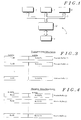
- a host processor 4 transmits messages to and receives messages from peripheral devices 6-8 via a message communication interface 10 and a serial bus 9.
- each one of the transmit and receive messages is a fixed length message comprising an ID field TxID, RxID of m bits and a data field TxDATA, RxDATA of n bits.
- ID fields of the stored messages to be transmitted are used to prioritise the messages to be transmitted by the message communication interface.
- the ID field of each of the received messages is used to determine whether the message is to be received by the interface.
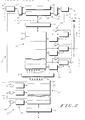
- the message communication system 12 comprises a four-port storage portion 13 and a serial output portion 15.
- the four-port storage portion 13 is implemented in Random Access Memory (RAM) and has a first parallel port 18 for coupling to the host processor via a data bus, a second parallel port 44 for coupling to the serial output portion 15 and first 17 and second 19 serial ports coupled to the serial output portion 15.
- the serial output portion 15 comprises a transmit pin 14 and a receive pin 16 for coupling to the peripheral devices 6-8 via serial bus 9.
- the storage portion 13 comprises transmit buffers 20 for storing messages to be transmitted by the message communication system 12 and receive buffers 22 for storing messages received by the message communication system 12.
- the transmit 20 and the receive 22 buffers are implemented in RAM.
- the transmit buffers 20 can store up to t messages and the receive buffers 22 can store up to r received messages.
- Both buffers 20 and 22 are arranged to store the m-bit ID of a message in an ID storage field 24 and the associated n-bit data in a data storage field 26.
- the structure of the message communication system 12 in accordance with the invention will be described in more detail with reference to a transmit operation, during which the host transmits messages to the peripheral devices, and a receive operation, during which the message communication system receives messages from the peripheral devices for the host.
- the host sends messages to the message communication system 12 via the host data bus and port 18.
- the ID and data of the sent messages are written to the transmit buffers 20.
- Each transmit buffer which is written to becomes an 'active transmit buffer'.
- the message communication system 12 is enabled for a transmit operation in response to detecting that the serial bus 9 is free when it has a message to be transmitted.
- An arbitration process is carried out to determine which one of the active transmit buffers has the highest priority: that is, which of the stored transmit messages has the highest priority.
- the arbitration process utilises the IDs of the stored transmit messages to determine which of the messages is to be transmitted first on the serial bus 9.
- the arbitration process is performed bit serially through m cycles using arbitration logic 28.
- the arbitration logic 28 comprises t comparators 32 and t flag generators 34. Each one of the comparators having a first input coupled to a respective one of the ID storage fields 24, a second input coupled to wired AND logic 30, and an output coupled to a respective one of the flag generators 34.
- Each one of the flag generators 34 generates a transmit ID flag which is coupled to a respective one of the data storage fields 26. Initially, each transmit ID flag is set to '1' (winner).
- an ID bit is read from each of the active transmit buffers and logically combined with the other ID bits read from the other active transmit buffers in the wired AND logic 30.
- the Most Significant Bit (MSB) of the m ID bits is read first.
- Each of the read ID bits is compared to the 'wired AND' result in a respective one of the t comparators 32 and a transmit ID flag generated in dependence on the output of the respective comparator. If the bit read from an active transmit buffer is recessive and the wired AND result dominant, then that transmit buffer 'loses', the transmit ID flag is reset to '0' (loser) and the transmit buffer is ignored in the next arbitration cycle.
- the wired AND result whose value represents the value of the 'winning' ID bits, is shifted via a switch 42 to an ID shift register 38 of a transmit/receive shifter 36 in serial output portion 15. The cycle is then repeated without the losing active transmit buffers.
- the arbitration process is complete and the ID shift register 38 contains the ID of the active transmit buffer having the highest priority: that is, the ID of the winning transmit buffer.
- the transmit ID flag of the winning active transmit buffer is set to '1' and the data stored in the data storage field 26 of the winning active transmit buffer is loaded in parallel via the data port 44 and n-bit bus 45 to a data shift register 40 of the transmit/receive shifter 36. Once all the n bits of data are loaded into the data shift register 40, the 'winning' message is transmitted to the serial bus 9.
- additional logic selects the lower of the two active transmit buffers for transmission.
- the 'winning' message in the transmit/receive shifter 36 is transmitted to the serial bus 9, via a switch 46, transmit logic 47 which converts the 'winning' message according to the protocol of the serial bus 9, and the transmit pin 14, by first shifting-out the 'winning' ID from the ID shift register 38, starting with the Most Significant Bit (MSB), and then shifting-out the 'winning' data from the data shift register 40.
- the message communication system has a 'self-listening' function which means that the bits shifted-out to the serial bus return bit serially through the receiver pin 16 and into the same transmit/receive shifter 36 via the switch 42 and receive logic 43.
- the switches 42 and 46 select between the transmit ID or data or between the received ID or data.
- the storage portion 13 further comprises read select logic 21 which successively selects each bit of the transmit or receive buffers for transmission or reception respectively.
- the read select logic 21 is implemented as a 'marching '1" shift register.
- the host writes the m-bit IDs of the messages to be received by the message communication system 12 to the ID storage fields 24 of a predetermined number of the receive buffers 22. Writing an ID to a receive buffer activates that receive buffer.
- Logic for determining whether a message is to be received and stored by the message communication system 12 comprises r comparators 48 and r match flag generators 50.
- Each of the r comparators 48 has a first input coupled to receive the ID bits of the received message, a second input coupled to the ID storage field 24 of a respective one of the receive buffers 22 and an output coupled to a respective one of the match flag generators.
- Each one of the match flag generators 50 generates a receive ID flag which is coupled to a respective one of the data storage fields 26 of the receive buffers 22. Initially, each receive ID flag is set to '1' (match).
- a message is received at the receive pin 16 and serially shifted into the transmit/receive shifter 36 via the switch 42.
- the ID bits of the incoming message are received first.
- each received bit is simultaneously coupled via switch 46 to each one of the r comparators 48.
- Each one of the comparators of the active receive buffers compares each received ID bit with the corresponding ID bits from the respective active receive buffer and provides an output to the respective match flag generator. For each comparison, if there is no match, the respective ID flag is cleared to '0' and if there is a match, the respective ID flag is left set to '1'.
- each comparator comprises an exclusive OR gate. If the ID bits match, the output of the exclusive OR gate does not reset the receive ID flag. If the ID bits do not match, the output of the exclusive OR gate resets the receive ID flag to '0'.
- the n data bits are written, via data port 44, simultaneously to the data storage fields 26 of the active receive buffers having receive ID flags set to '1'.
- the host can then read the incoming messages stored in the active receive buffers 22.
- the present invention utilises a parallel port for transferring data between the storage portion 13 and the serial output portion 15, but serial ports 17 and 19 for transferring the ID bits serially between the storage portion 13 and the serial output portion 15. This ensures significant space saving.
- the message communication system in accordance with the present invention provides a system for transmitting and receiving messages using RAM-based storage buffers having two parallel ports and two serial ports.
- the serial ports transfer serially the ID bits of the transmitted and received messages.
- Logic is used to determine, from the ID bits, which message of the messages to be transmitted has the highest priority and to provide the ID bits of the highest priority message serially to one of the serial ports.
- Additional logic receives the ID bits of the received messages serially from the other serial port and determines whether the messages are to be stored in the RAM-based storage buffer, by comparing the received ID bits with previously stored ID bits.
- the transmit message prioritising and the received messages ID comparing steps are both performed bit serially in m cycles (where m is the number of ID bits) using simple logic and thus, are relatively fast but require minimal hardware to implement.
- the same compact RAM structure can be used for the transmit buffers and the receive buffers.
- a further advantage of the message communication system in accordance with the present invention is that only one shifter is used by both the receiver and transmitter of the system. No additional latches or temporary registers are needed to store the ID or data, or to store an intermediate result of the ID transmit message prioritising step or the received message ID comparing step.
Landscapes
- Engineering & Computer Science (AREA)
- Computer Networks & Wireless Communication (AREA)
- Signal Processing (AREA)
- Communication Control (AREA)
- Information Transfer Systems (AREA)
Description
and
ELEKTRONIK, vol.38, no.4, 17 February 1989, MÜNCHEN, DE pages 102 - 105 F. BEIL ET AL 'Eine bitserielle Universal-Schnittstelle nicht nur für Kfz-Anwendungen' in such applications utilises messages for communicating data between the host and peripherals wherein each message comprises an n-bit data field and an m-bit identifier field (where n and m are positive integers). The data field contains the data to be transferred by the message and the identifier (ID) field categorises the data in each message. For example, all data relating to temperature has a unique ID.
| ID Bit Value | AND Result | Action | Transmit ID Flag Value |
| 0 | 0 | non | 1 |
| 1 | 0 | lose | 0 |
| 1 | 1 | non | 1 |
Claims (13)
- A message communication system for receiving, storing and transmitting messages, wherein each message comprises ID information and data, the ID information of each message providing an indication of the priority of each message, characterized in that the message communication system comprises :serial output means (15) having an input (16) for receiving messages and an output (14) for transmitting messages;RAM storage means (13) for storing messages received by the serial output means (15) and transmit messages to be transmitted by the serial output means (15), the RAM storage means (13) having a first port (44) coupled to the serial output means (15) for transferring the data of the received and transmit messages between the serial output means (15) and the RAM storage means (13), a second port (18) for transferring messages to and from the message communication system, a third port (19) for serially transferring ID information of transmit messages from the RAM storage means (13) to the serial output means (15) and a fourth port (17) for serially transferring ID information of received messages from the serial output means (15) to the RAM storage means (13), the RAM storage means (13) further comprising:first logic means (28) coupled to receive the ID information of each of the stored transmit messages for determining the stored transmit message with the greatest priority and for generating a signal in response thereto whereby the data of the determined transmit message is transferred from the RAM storage means (13) to the serial output means (15), the ID of the determined transmit message is transferred serially to the serial output means (15) via the third port (19); andsecond logic means (48,50,21) coupled to the fourth port (17) so as to receive the ID information of the received messages for determining which of the received messages are to be stored in the RAM storage means (13) and for generating a signal in response thereto whereby the data of the determined received messages is transferred from the serial output means (15) via the first port (44) to the RAM storage means (13) for storage therein.
- The message communication system according to claim 1 wherein the ID information comprises m ID bits and the first logic means (28) determines the stored transmit message with the greatest priority in m cycles by comparing in m consecutive cycles each ID bit of a stored transmit message with the corresponding ID bits of the other stored messages, and by outputting to the serial output means (15) via the third port (19) after each consecutive comparison the ID bit with the determined greatest priority.
- The message communication system according to claim 1 wherein the ID information comprises m ID bits and the first logic means (28) comprises:means for logically combining (30) in m consecutive cycles each of the m ID bits of a stored transmit message with the corresponding ID bits of other stored transmit messages and for providing a result bit for each consecutive combination, each result bit being serially transferred to the serial output means (15) via the third port (19);means for comparing (32) each one of the combined ID bits with the corresponding result bit and for providing a comparison result for the respective stored transmit message for each consecutive combination; andmeans for generating a flag (34) for each stored transmit message, each flag being switchable from a first state to a second state in dependence on the comparison results, wherein after the m consecutive cycles the stored transmit message with a flag having the first state corresponds to the determined transmit message and the result bits transferred to the serial output means (15) represent the ID information of the determined transmit message.
- The message communication system according to claim 3 wherein the means for logically combining (30) in response to the flag of a stored transmit message being switched from the first state to the second state, ignores the ID bits of the switched stored transmit message in following cycles.
- The message communication system according to claim 3 or 4 wherein the means for logically combining (30) comprises wired AND logic.
- The message communication system according to claim 5 wherein the comparing means (32) provides a comparison result having a first value when the combined ID bit of a stored transmit message matches the result bit and a second value when the combined ID bit does not match the result bit and wherein the flag generating means (34) switches the flag from the first state to the second state when the comparison result has the second value.
- The message communication system according to any preceding claim wherein the RAM storage means (13) comprises a receive buffer means (22) for storing the received messages and a transmit buffer means (20) for storing the transmit messages.
- The message communication system according to claim 7 wherein each buffer means (20,22) comprises a plurality of message storage locations, each message storage location comprising an ID storage field (24) for storing the ID information and a data storage field (26) for storing the data.
- The message communication system according to claim 3 and claim 7 or 8 wherein the comparing means (32) comprises a plurality of comparators corresponding to the plurality of message storage locations of the transmit buffer means (22), each comparator having a first input coupled to a respective ID storage field (24), a second input coupled to the means for logically combining (30) and an output coupled to the flag generating means (34).
- The message communication system according to any preceding claim wherein the ID information comprises m ID bits and the RAM storage means (13) stores predetermined ID informations received via the second port (18) and wherein the second logic means (48,50,21) comprises comparing means (48) for serially comparing each of the m ID bits of the received messages with corresponding ID bits of the predetermined ID informations, the second logic means (48,50,21) generating the signal when the ID bits of the received messages match the ID bits of at least one of the predetermined ID informations stored in the RAM storage means (13).
- The message communication system according to claim 8 and 10 wherein the predetermined ID informations are stored in ID storage fields (24) of the receive buffer means (22) and the comparing means of the second logic means comprises a plurality of comparators (48) corresponding to the plurality of message storage locations of the receive buffer means (22), each comparator (48) having a first input coupled to the fourth port (17), a second input coupled to a respective ID storage field (24) and an output coupled to a match flag generating means (50), the match flag generating means (50) generating a flag for each storage location of the receive buffer means (22), each flag being switchable from a first state which indicates a match comparison result to a second state which indicates a no-match comparison result in dependence on the output of the respective comparator, wherein after m consecutive comparison cycles the second logic means (48,50) generates the signal for the storage locations with flags having the first state whereby data of the received message is transferred from the serial output means to the data storage fields (26) of of the storage locations with flags having the first state.
- The message communication system according to any preceding claims wherein the serial output means (15) comprises a first shift register (40) for serially transferring data and a second shift register (38) for serially transferring ID information.
- A processing system (2) comprising:a host processor (4);a plurality of peripheral devices (6-8);a message communication system (10,12) as claimed in any preceding claim for transferring messages between the host processor (4) and the peripheral devices (6-8), a serial output means of the message communication system being coupled to the plurality of peripheral devices (6-8) via a serial bus (9) and the host processor (4) being coupled to the second port of the message communication system (12).
Applications Claiming Priority (2)
| Application Number | Priority Date | Filing Date | Title |
|---|---|---|---|
| GB9308442 | 1993-04-23 | ||
| GB9308442A GB2277425B (en) | 1993-04-23 | 1993-04-23 | Message communication system |
Publications (2)
| Publication Number | Publication Date |
|---|---|
| EP0621709A1 EP0621709A1 (en) | 1994-10-26 |
| EP0621709B1 true EP0621709B1 (en) | 1998-08-05 |
Family
ID=10734366
Family Applications (1)
| Application Number | Title | Priority Date | Filing Date |
|---|---|---|---|
| EP19940104170 Expired - Lifetime EP0621709B1 (en) | 1993-04-23 | 1994-03-17 | Message communication system |
Country Status (4)
| Country | Link |
|---|---|
| EP (1) | EP0621709B1 (en) |
| DE (1) | DE69412164T2 (en) |
| ES (1) | ES2118998T3 (en) |
| GB (1) | GB2277425B (en) |
Families Citing this family (15)
| Publication number | Priority date | Publication date | Assignee | Title |
|---|---|---|---|---|
| GB2301712B (en) * | 1995-06-02 | 2000-02-23 | Dsc Communications | Integrated directional antenna |
| US5915216A (en) * | 1995-06-02 | 1999-06-22 | Dsc Communications Corporation | Apparatus and method of transmitting and receiving information in a wireless telecommunications system |
| US5742595A (en) * | 1995-06-02 | 1998-04-21 | Dsc Communications Corporation | Processing CDMA signals |
| GB2302240B (en) * | 1995-06-02 | 2000-01-12 | Dsc Communications | Apparatus and method of frame aligning information in a wireless telecommunications system |
| GB2301751B (en) * | 1995-06-02 | 2000-02-09 | Dsc Communications | Control message transmission in telecommunications systems |
| US5745496A (en) * | 1995-06-02 | 1998-04-28 | Dsc Communications Corporation | Apparatus and method of establishing a downlink communication path in a wireless telecommunications system |
| GB2301752B (en) * | 1995-06-02 | 2000-03-29 | Dsc Communications | Control message transmission in telecommunications systems |
| GB2301717B (en) * | 1995-06-02 | 1999-08-11 | Dsc Communications | Network controller for monitoring the status of a network |
| GB2301735B (en) * | 1995-06-02 | 1999-07-28 | Dsc Communications | Message handling in a telecommunications network |
| US5696766A (en) * | 1995-06-02 | 1997-12-09 | Dsc Communications Corporation | Apparatus and method of synchronizing a transmitter in a subscriber terminal of a wireless telecommunications system |
| US5809093A (en) * | 1995-06-02 | 1998-09-15 | Dsc Communications Corporation | Apparatus and method of frame aligning information in a wireless telecommunications system |
| JP3529588B2 (en) | 1997-05-30 | 2004-05-24 | インターナショナル・ビジネス・マシーンズ・コーポレーション | Computer network system, computer, computer for temporary storage, and method in these |
| US6510479B1 (en) * | 1999-09-15 | 2003-01-21 | Koninklijke Philips Electronics N.V. | Transmit pre-arbitration scheme for a can device and a can device that implements this scheme |
| US7975120B2 (en) | 2006-12-27 | 2011-07-05 | Freescale Semiconductor, Inc. | Dynamic allocation of message buffers |
| GB2547959B (en) * | 2016-01-08 | 2020-07-08 | Cummins Inc | Communication interface for start-stop systems and methods |
Family Cites Families (3)
| Publication number | Priority date | Publication date | Assignee | Title |
|---|---|---|---|---|
| US4604683A (en) * | 1984-12-10 | 1986-08-05 | Advanced Computer Communications | Communication controller using multiported random access memory |
| US4996666A (en) * | 1988-08-12 | 1991-02-26 | Duluk Jr Jerome F | Content-addressable memory system capable of fully parallel magnitude comparisons |
| US5151895A (en) * | 1990-06-29 | 1992-09-29 | Digital Equipment Corporation | Terminal server architecture |
-
1993
- 1993-04-23 GB GB9308442A patent/GB2277425B/en not_active Expired - Fee Related
-
1994
- 1994-03-17 EP EP19940104170 patent/EP0621709B1/en not_active Expired - Lifetime
- 1994-03-17 ES ES94104170T patent/ES2118998T3/en not_active Expired - Lifetime
- 1994-03-17 DE DE1994612164 patent/DE69412164T2/en not_active Expired - Fee Related
Also Published As
| Publication number | Publication date |
|---|---|
| DE69412164D1 (en) | 1998-09-10 |
| EP0621709A1 (en) | 1994-10-26 |
| ES2118998T3 (en) | 1998-10-01 |
| GB2277425A (en) | 1994-10-26 |
| GB9308442D0 (en) | 1993-06-09 |
| DE69412164T2 (en) | 1999-03-04 |
| GB2277425B (en) | 1997-08-06 |
Similar Documents
| Publication | Publication Date | Title |
|---|---|---|
| EP0018755B1 (en) | Digital communication networks employing speed independent switches | |
| US4742349A (en) | Method for buffered serial peripheral interface (SPI) in a serial data bus | |
| EP0621709A1 (en) | Message communication system | |
| US6122667A (en) | Method and integrated circuit for high-bandwidth network server interfacing to a local area network using CSMA/CD | |
| CN102326363B (en) | Microcontroller with can module using buffer description table | |
| US5619722A (en) | Addressable communication port expander | |
| CA1185375A (en) | Dual path bus structure for computer interconnection | |
| US7979594B2 (en) | Serial communications device with dynamic allocation of acceptance masks using serial implementation | |
| EP0018756B1 (en) | Speed independent arbiter switch for digital communication networks | |
| JPH06261052A (en) | Flow control device of shared bus | |
| US5502817A (en) | Ultra high speed data collection, processing and distribution ring with parallel data paths between nodes | |
| US6944739B2 (en) | Register bank | |
| CN100586092C (en) | Serial communication device with dynamic filter assignment | |
| US6912594B2 (en) | Serial communication device with multi-mode operation of message receive buffers | |
| US6912566B1 (en) | Memory device and method for operating the memory device | |
| US5369755A (en) | Computer communication bus system using multiple content induced transaction overlap (CITO) communication channels | |
| EP0789303B1 (en) | Memory system and a data communication system | |
| US20030056016A1 (en) | Serial communication device with dynamic filter allocation | |
| CN111832048A (en) | Data packet ordering method and system based on dual-port RAM | |
| US5481753A (en) | I/O device having identification register and data register where identification register indicates output from the data register to be an identifier or normal data | |
| US5056012A (en) | Memory addressable data transfer network | |
| US20040066791A1 (en) | Asynchronous expansible switching system for switching packet with different length | |
| US6282203B1 (en) | Packet data transmitting apparatus, and method therefor | |
| US5909558A (en) | Low power serial arbitration system | |
| JPH0225579B2 (en) |
Legal Events
| Date | Code | Title | Description |
|---|---|---|---|
| PUAI | Public reference made under article 153(3) epc to a published international application that has entered the european phase |
Free format text: ORIGINAL CODE: 0009012 |
|
| AK | Designated contracting states |
Kind code of ref document: A1 Designated state(s): DE ES FR IT NL SE |
|
| 17P | Request for examination filed |
Effective date: 19950426 |
|
| GRAG | Despatch of communication of intention to grant |
Free format text: ORIGINAL CODE: EPIDOS AGRA |
|
| 17Q | First examination report despatched |
Effective date: 19970930 |
|
| GRAG | Despatch of communication of intention to grant |
Free format text: ORIGINAL CODE: EPIDOS AGRA |
|
| GRAH | Despatch of communication of intention to grant a patent |
Free format text: ORIGINAL CODE: EPIDOS IGRA |
|
| GRAH | Despatch of communication of intention to grant a patent |
Free format text: ORIGINAL CODE: EPIDOS IGRA |
|
| GRAA | (expected) grant |
Free format text: ORIGINAL CODE: 0009210 |
|
| ITF | It: translation for a ep patent filed | ||
| AK | Designated contracting states |
Kind code of ref document: B1 Designated state(s): DE ES FR IT NL SE |
|
| REF | Corresponds to: |
Ref document number: 69412164 Country of ref document: DE Date of ref document: 19980910 |
|
| REG | Reference to a national code |
Ref country code: ES Ref legal event code: FG2A Ref document number: 2118998 Country of ref document: ES Kind code of ref document: T3 |
|
| ET | Fr: translation filed | ||
| PLBE | No opposition filed within time limit |
Free format text: ORIGINAL CODE: 0009261 |
|
| STAA | Information on the status of an ep patent application or granted ep patent |
Free format text: STATUS: NO OPPOSITION FILED WITHIN TIME LIMIT |
|
| 26N | No opposition filed | ||
| PGFP | Annual fee paid to national office [announced via postgrant information from national office to epo] |
Ref country code: NL Payment date: 20050209 Year of fee payment: 12 |
|
| PGFP | Annual fee paid to national office [announced via postgrant information from national office to epo] |
Ref country code: SE Payment date: 20050303 Year of fee payment: 12 |
|
| PGFP | Annual fee paid to national office [announced via postgrant information from national office to epo] |
Ref country code: ES Payment date: 20050318 Year of fee payment: 12 |
|
| NLS | Nl: assignments of ep-patents |
Owner name: FREESCALE SEMICONDUCTOR, INC. Effective date: 20051028 |
|
| PG25 | Lapsed in a contracting state [announced via postgrant information from national office to epo] |
Ref country code: SE Free format text: LAPSE BECAUSE OF NON-PAYMENT OF DUE FEES Effective date: 20060318 Ref country code: ES Free format text: LAPSE BECAUSE OF NON-PAYMENT OF DUE FEES Effective date: 20060318 |
|
| PGFP | Annual fee paid to national office [announced via postgrant information from national office to epo] |
Ref country code: IT Payment date: 20060331 Year of fee payment: 13 |
|
| PG25 | Lapsed in a contracting state [announced via postgrant information from national office to epo] |
Ref country code: NL Free format text: LAPSE BECAUSE OF NON-PAYMENT OF DUE FEES Effective date: 20061001 |
|
| EUG | Se: european patent has lapsed | ||
| NLV4 | Nl: lapsed or anulled due to non-payment of the annual fee |
Effective date: 20061001 |
|
| PGFP | Annual fee paid to national office [announced via postgrant information from national office to epo] |
Ref country code: DE Payment date: 20070330 Year of fee payment: 14 |
|
| REG | Reference to a national code |
Ref country code: ES Ref legal event code: FD2A Effective date: 20060318 |
|
| PGFP | Annual fee paid to national office [announced via postgrant information from national office to epo] |
Ref country code: FR Payment date: 20070301 Year of fee payment: 14 |
|
| REG | Reference to a national code |
Ref country code: FR Ref legal event code: ST Effective date: 20081125 |
|
| PG25 | Lapsed in a contracting state [announced via postgrant information from national office to epo] |
Ref country code: DE Free format text: LAPSE BECAUSE OF NON-PAYMENT OF DUE FEES Effective date: 20081001 |
|
| PG25 | Lapsed in a contracting state [announced via postgrant information from national office to epo] |
Ref country code: FR Free format text: LAPSE BECAUSE OF NON-PAYMENT OF DUE FEES Effective date: 20080331 |
|
| PG25 | Lapsed in a contracting state [announced via postgrant information from national office to epo] |
Ref country code: IT Free format text: LAPSE BECAUSE OF NON-PAYMENT OF DUE FEES Effective date: 20070317 |