EP0613262B1 - Source de bruit optique - Google Patents
Source de bruit optique Download PDFInfo
- Publication number
- EP0613262B1 EP0613262B1 EP94200207A EP94200207A EP0613262B1 EP 0613262 B1 EP0613262 B1 EP 0613262B1 EP 94200207 A EP94200207 A EP 94200207A EP 94200207 A EP94200207 A EP 94200207A EP 0613262 B1 EP0613262 B1 EP 0613262B1
- Authority
- EP
- European Patent Office
- Prior art keywords
- optical
- input
- light source
- signal
- noise
- Prior art date
- Legal status (The legal status is an assumption and is not a legal conclusion. Google has not performed a legal analysis and makes no representation as to the accuracy of the status listed.)
- Expired - Lifetime
Links
Images
Classifications
-
- H—ELECTRICITY
- H04—ELECTRIC COMMUNICATION TECHNIQUE
- H04B—TRANSMISSION
- H04B10/00—Transmission systems employing electromagnetic waves other than radio-waves, e.g. infrared, visible or ultraviolet light, or employing corpuscular radiation, e.g. quantum communication
- H04B10/50—Transmitters
Definitions
- the invention relates to an optical noise source comprising
- narrowband light source means which comprise a laser diode (narrowband light source) for generating a narrowband optical signal.
- the anode (base input) of the laser diode is fed with a sinusoidal current (electrical periodic signal) with which the narrowband optical signal is modulated.
- Said modulated optical signal is fed to an interference filter which consists of two 3 dB couplers with, therebetween, two pieces of glass fibre having a mutual path length difference of approximately 1 km.
- the interference filter generates the optical composition signal which is composed of two mutually different frequency-modulated signals.
- an electrical photodiode noise signal is produced whose (electrical) noise bandwidth is equal to the maximum instantaneous frequency difference between the two optical signals. If the spectrum of the electrical photodiode noise signal is to be as flat as possible within the chosen noise bandwidth (which is specified with the amplitude of the electrical periodic signal), the path length difference on which the interference filter is based must be considerably larger than the coherence length of the light source.
- Said coherence length, for the present-generation laser diodes for example, is 10 metres and may increase to several kilometres for modern multi-section lasers.
- This known noise source has the drawback that the interference filter needs to be based on a large path length difference (such as, for example, 1 kilometre).
- the object of the invention is, inter alia, to provide a noise source of the type mentioned in the preamble, in which it is sufficient to use an interference filter based on a considerably smaller path length difference (of, for example, 10 metres).
- the noise source according to the invention is characterized in that the narrowband light source means are provided with a noise input for receiving an electrical noise signal.
- the linewidth of the optical signal which may or may not already have been modulated, increases, which corresponds to a decrease in the coherence length of the narrowband light source used, as a result of which it is sufficient to use an interference filter which is based on a smaller path length difference of, for example, a few metres.
- the invention is based on the insight that the coherence length of a narrowband light source is inversely proportional to the linewidth of the optical signal of said light source, and that a large coherence length (and thus a small linewidth) requires a relatively large difference in delay time in the interference filter, if the spectrum of the electrical photodiode noise signal is to be as flat as possible over the chosen noise bandwidth.
- This relatively large difference in delay time in the interference filter is implemented by means of a large path length difference, and requires a relatively low modulation frequency in order to make the maximum instantaneous frequency difference between the interfering optical signals equal to the optical frequency swing.
- the noise bandwidth reaches a maximum, equal to the available optical frequency swing.
- a first embodiment of the noise source according to the invention is characterized in that a bandwidth of the electrical noise signal is smaller than a frequency of the electrical periodic signal.
- the electrical noise signal to be supplied to the narrowband light source means being limited in frequency, for example via a fourth-order low-pass filter, the concentration of noise power in the chosen noise bandwidth increases, owing to which noise power is handled more efficiently and less noise power is wasted outside the chosen noise bandwidth.
- a second embodiment of the noise source according to the invention is characterized in that the electrical periodic signal is triangular.
- a triangular electrical periodic signal results, compared to a sinusoidal electrical periodic signal having a comparable amplitude, in an electrical photodiode noise signal which can be considered as flat over a larger part of the noise bandwidth.
- a third embodiment of the noise source according to the invention is characterized in that the optical noise source comprises an optical detector for detecting at least a part of the optical composition signal, which optical detector is coupled, via a filter, to an input of the narrowband light source means.
- the optical signal coming from the narrowband light source means is stabilized, which is of great importance for certain measurements.
- a fourth embodiment of the noise source according to the invention is characterized in that the filter is a high-pass or bandpass filter with which an electrical detector is cascaded for controlling the electrical periodic signal, the input of the narrowband light source means being the base input.
- the (positive) feedback via a bandpass or high-pass filter and a detector for controlling the electrical periodic signal stabilizes the spectral noise density of the electrical photodiode noise signal.
- Controlling in this case may comprise regulating the amplitude and/or regulating the frequency of the electrical periodic signal.
- a fifth embodiment of the noise source according to the invention is characterized in that the filter is a low-pass filter for regulating a power level of the optical signal, the input of the narrowband light source means being a power input.
- a sixth embodiment of the light source according to the invention is characterized in that the narrowband light source means comprise an optical input for receiving the narrowband optical signal.
- the narrowband light source means therefore do not comprise a light source but are fed with the narrowband optical signal via the optical input.
- a seventh embodiment of the noise source according to the invention is characterized in that the narrowband light source means comprise an optical modulator which is optically coupled to the optical input and of which an input forms the base input.
- the narrowband optical signal received via the optical input is modulated in frequency.
- modulation is likewise possible, such as, for example, phase modulation.
- An eighth embodiment of the noise source according to the invention is characterized in that the narrowband light source means comprise an optical modulator which is optically coupled to the optical input and of which an input forms the noise input.
- the narrowband optical signal received via the optical input is modulated in frequency with said electrical noise signal. This can take place both before and after the narrowband optical signal is frequency-modulated with the electrical periodic signal.
- modulation are likewise possible, such as, for example, phase modulation.
- a ninth embodiment of the noise source according to the invention is characterized in that the narrowband light source means comprise an optical amplitude modulator which is optically coupled to the optical input and of which an input forms a power input.
- the narrowband optical signal received via the optical input is amplitude-modulated with said electrical DC signal. This is done to adjust the power level of the narrowband optical signal to be generated by the narrowband light source means. This can take place both before and after the narrowband optical signal is frequency-modulated with the electrical periodic signal and is modulated with the electrical noise signal.
- a tenth embodiment of the noise source according to the invention is characterized in that the narrowband light source means comprise a narrowband light source for generating the narrowband optical signal.
- the narrowband light source means therefore comprise the narrowband light source which generates the narrowband optical signal.
- An eleventh embodiment of the noise source according to the invention is characterized in that the narrowband light source means comprise an optical modulator which is optically coupled to the narrowband light source and of which an input forms the base input.
- the narrowband optical signal to be generated by the narrowband light source is frequency-modulated.
- a twelfth embodiment of the noise source according to the invention is characterized in that the narrowband light source means comprise an optical modulator which is optically coupled to the narrowband light source and of which an input forms the noise input.
- the narrowband optical signal to be generated by the narrowband light source is modulated with said electrical noise signal. This may take place both before and after the narrowband optical signal is frequency-modulated with the electrical periodic signal.
- a thirteenth embodiment of the noise source according to the invention is characterized in that the narrowband light source means comprise an optical amplitude modulator which is optically coupled to the input of the narrowband light source and of which an input forms a power input.
- the narrowband optical signal received via the optical input is amplitude-modulated with said electrical DC signal. This is done to adjust the power level of the narrowband optical signal to be generated by the narrowband light source means. This can take place both before and after the narrowband optical signal is frequency-modulated with the electrical periodic signal and is modulated with the electrical noise signal.
- a fourteenth embodiment of the noise source according to the invention is characterized in that the narrowband light source is provided with an input which forms the base input.
- the narrowband light source is itself provided with the base input, thus saving a modulator.
- a fifteenth embodiment of the noise source according to the invention is characterized in that the narrowband light source is provided with an input which forms the noise input.
- the narrowband light source is itself provided with the noise input, thus saving a modulator.
- a sixteenth embodiment of the noise source according to the invention is characterized in that the narrowband light source is provided with an input which forms a power input.
- the narrowband light source is itself provided with the power input, thus saving an amplitude modulator.
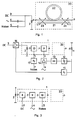
- the first optical noise source depicted in Figure 1 comprises a narrowband light source 2 such as, for example, a laser diode, of which the cathode is connected to ground and of which the anode forms a power input 3 for receiving an electrical DC signal. Said anode further forms, via a first capacitor, a base input 4 for receiving an electrical periodic signal (such as, for example, a sinusoidal signal for the purpose of frequency modulation of a narrowband optical signal to be emitted by the narrowband light source 2) and further forms, via a second capacitor, a noise input 5 for receiving an electrical noise signal.
- the first optical noise source depicted in Figure 1 further comprises an interference filter 20, based on path length difference, for receiving the modulated optical signal and for generating an optical composition signal.
- Said interference filter 20 comprises, for example, a first glass fibre 21 and a second glass fibre 22 which has a greater length than glass fibre 21. Both glass fibres 21, 22 are coupled to one another at a receiving side via a 3 dB coupler 23 and are coupled to one another, at an emitting side, via a 3 dB coupler 24.
- the narrowband light source 2 forms the narrowband light source means.
- the power of the light source 2 is adjusted, and by means of the periodic signal to be fed to base input 4, the optical signal is modulated.
- the modulated optical signal is split in the 3 dB coupler 23 in the interference filter 20. Owing to the optical signals thus split off each covering a different path length in the glass fibres 21, 22 and then being combined in the 3 dB coupler 24, the interference filter 20 generates the composition signal which is formed by two different frequency-modulated optical signals.
- an electrical photodiode noise signal is produced whose (electrical) noise bandwidth is equal to the largest instantaneous frequency difference between the optical signals at the ends of the glass fibres 21, 22. Said frequency difference is at a maximum if the period of the electrical periodic signal is chosen to be equal to twice the delay time of the interference filter 20.
- the path length difference on which the interference filter 20 is based must be considerably greater than the coherence length of the light source 2.
- the linewidth of the optical signal increases, which corresponds to a decrease in the coherence length of the light source 2, as a result of which it is sufficient to use a shorter delay time and thus a smaller path length difference in the interference filter 20 and thus a higher modulation frequency of the periodic signal. Consequently, the required path length difference in the interference filter decreases substantially, which is of great advantage in various respects (such as costs and handling).
- the laser diode 2 is a modern multi-section laser which can more readily be frequency-modulated than, for example, a DFB (distributed feedback) laser and which is equipped with separate inputs for power modulation and frequency modulation, a variation in the optical frequency will be associated with a considerably smaller parasitic variation in the optical power, which is obviously advantageous. Without the noise signal being fed in, the desired path length difference in the interference filter 20, when using this modern multi-section laser, would have become unacceptably large.
- DFB distributed feedback
- the second optical noise source depicted in Figure 2 comprises narrowband light source means 1 which comprise the narrowband light source 2, an optical modulator 10, which is optically coupled to the narrowband light source 2 and has a noise input 5, and an optical modulator 9 which is optically coupled (via the optical modulator 10) to the narrowband light source 2 and has a base input 4.
- the second optical noise source depicted in Figure 2 further comprises the interference filter 20, based on path length difference, for receiving the modulated optical signal and for generating the optical composition signal.
- the cathode of the narrowband light source 2 is connected to ground, and the anode is connected to an output of an adjustable amplifier/attenuator circuit 16, of which an input forms the power input 3.
- Said second optical noise source is also equipped with an optical detector 11 such as, for example, a photodiode with associated electronics, for detecting at least part of the optical composition signal.
- Optical detector 11 is coupled to a low-pass filter 15 which is coupled to a control input of the adjustable amplifier/attenuator circuit 16 and is coupled, via a bandpass filter 12, to an input of an electrical detector 13, of which an output is coupled to a control input of an adjustable amplifier/attenuator circuit 14.
- An output of adjustable amplifier/attenuator circuit 14 is connected to the base input 4, and an input of adjustable amplifier/attenuator circuit 14 forms a further base input 6 for receiving the electrical periodic signals.
- Said second optical noise source further comprises a low-pass filter 17 which is situated between the noise input 5 and a further noise input 7 for receiving the noise signal.
- the power of the light source 2 is adjusted via the adjustable amplifier/attenuator circuit 16 which itself is adjusted via the control input.
- an increase in the signal power level detected by the photodiode 11 should result in an increase in the attenuation or a decrease in the gain of the adjustable amplifier/attenuator circuit 16, and a decrease in the signal power level detected by the photodiode 11 should result in a decrease in the attenuation or an increase in the gain of the adjustable amplifier/attenuator circuit 16 (i.e. negative feedback).
- Such a feedback results in stabilization of the optical power level generated by the narrowband light source 2.
- the optical signal generated by the narrowband light source 2 is frequency-modulated with the noise signal, which, as reported earlier, makes it possible to shorten considerably the path length difference in the interference filter 20.
- the frequency of the noise signal By means of the low-pass filter 17, the concentration of noise power in the chosen noise bandwidth increases, as a result of which the noise power is handled more efficiently and less noise power is wasted outside the chosen noise bandwidth.
- the optical signal which has already been frequency-modulated with the noise signal, is further frequency-modulated with the periodic signal which is fed in via the adjustable amplifier/attenuator circuit 14.
- the latter is adjusted via the control input itself by means of the signal coming from the detector 13 (such as, for example, a top detector, a power detector or a true root mean square detector).
- a decrease in the signal power level detected by the photodiode 11 in a specified frequency band should result in an increase in the attenuation or a decrease in the gain of the adjustable amplifier/attenuator circuit 14, and an increase in the signal power level in this frequency band detected by the photodiode 11 should result in a decrease in the attenuation or an increase in the gain of the adjustable amplifier/attenuator circuit 14 (i.e. positive feedback).
- Such a feedback results in stabilization of the spectral noise density of the signal detected by the photodiode 11.
- a bandpass filter 12 it would also be possible to use a high-pass filter, if the bandwidth of photodiode 11 with the associated electronics or of detector 13 is significantly lower than the noise bandwidth.
- Feeding in a triangular electrical periodic signal in comparison results in a sinusoidal electrical periodic signal having an amplitude comparable to an electrical photodiode noise signal which can be regarded as flat over a larger part of the noise bandwidth.
- the sequential order of the two optical modulators 9, 10 is completely arbitrary. It would further be possible to combine the two optical modulators 9, 10 into one optical modulator having one input, which input, as depicted in Figure 1, is fed with the noise signal and the periodic signal via capacitors.
- Both adjustable amplifier/attenuator circuits 14, 16 can be implemented in a manner known to those skilled in the art, using, for example, commercially available ICs. Since the adjustment of the periodic signal can take place not only on the basis of amplitude variation, but, for example, also on the basis of frequency variation, the adjustable amplifier/attenuator circuit 14 could in that case be implemented, in a manner known to those skilled in the art, using an adjustable frequency filter. Amplifier/attenuator circuit 16 could obviously also be embodied, in a manner known to those skilled in the art, as an addition or subtraction circuit.
- the third optical noise source depicted in Figure 3 comprises narrowband light source means 1 which are equipped with an optical modulator 8 having a power input 3 for receiving the DC signal for amplitude modulation of an optical signal coming from the narrowband light source 2, with the optical modulator 9 having the base input 4 for receiving the electrical periodic signal, and with the optical modulator 10 having the noise input 5 for receiving the noise signal.
- the sequential order of the three optical modulators 8, 9, 10 is again completely arbitrary, and both optical modulators 9, 10 could be combined into one optical modulator having one input, which input, as depicted in Figure 1, is fed with the noise signal and the periodic signal via capacitors.
- Said third optical noise source further comprises the interference filter 20.
- the mode of operation is otherwise in accordance with the first optical noise source depicted in Figure 1 and the second optical noise source depicted in Figure 2, it obviously being possible to use, in the case of said third optical noise source, both feedbacks, low-pass filter 17 and sinusoidal or triangular periodic signals.
- the same measurement setup can be employed at different optical frequencies by replacing the external narrowband light source 2 by a different specimen having a different optical frequency.
Claims (17)
- Source de bruit optique comprenantun moyen de source de lumière à bande étroite destiné à générer un signal optique modulé et muni d'une entrée de base destinée à recevoir un signal électrique périodique en vue de moduler un signal optique à bande étroite, etun filtre à interférence, fondé sur une différence de longueurs des lignes, afin de recevoir le signal optique modulé et afin de générer un signal de composition optique, caractérisé en ce que le moyen de source de lumière à bande étroite est muni d'une entrée de bruit afin de recevoir un signal électrique de bruit.
- Source de bruit optique selon la revendication 1, caractérisée en ce qu'une bande passante du signal électrique de bruit est plus petite qu'une fréquence du signal électrique périodique.
- Source de bruit optique selon la revendication 1 ou 2, caractérisée en ce que le signal électrique périodique est triangulaire.
- Source de bruit optique selon la revendication 1, 2 ou 3, caractérisée en ce que la source de bruit optique comprend un détecteur optique destiné à détecter au moins une partie du signal de composition optique, lequel détecteur optique est relié, par l'intermédiaire d'un filtre, à une entrée du moyen de source de lumière à bande étroite.
- Source de bruit optique selon la revendication 4, caractérisée en ce que le filtre est un filtre passe-haut ou passe-bande avec lequel un détecteur électrique est mis en cascade afin de commander le signal électrique périodique, l'entrée du moyen de source de lumière à bande étroite étant l'entrée de base.
- Source de bruit optique selon la revendication 4, caractérisée en ce que le filtre est un filtre passe-bas destiné à réguler un niveau de puissance du signal optique, l'entrée du moyen de source de lumière à bande étroite étant une entrée de puissance.
- Source de bruit optique selon la revendication 1, 2, 3, 4, 5 ou 6, caractérisée en ce que le moyen de source de lumière à bande étroite comprend une entrée optique destinée à recevoir le signal optique à bande étroite.
- Source de bruit optique selon la revendication 7, caractérisée en ce que le moyen de source de lumière à bande étroite comprend un modulateur optique qui est couplé optiquement à l'entrée optique et dont une entrée constitue l'entrée de base.
- Source de bruit optique selon la revendication 7 ou 8, caractérisée en ce que le moyen de source de lumière à bande étroite comprend un modulateur optique qui est couplé optiquement à l'entrée optique et dont une entrée constitue l'entrée de bruit.
- Source de bruit optique selon la revendication 7, 8 ou 9, caractérisée en ce que le moyen de source de lumière à bande étroite comprend un modulateur d'amplitude optique qui est couplé optiquement à l'entrée optique et dont une entrée constitue une entrée de puissance.
- Source de bruit optique selon la revendication 1, 2, 3, 4, 5 ou 6, caractérisée en ce que le moyen de source de lumière à bande étroite comprend une source de lumière à bande étroite destinée à générer le signal optique à bande étroite.
- Source de bruit optique selon la revendication 11, caractérisée en ce que le moyen de source de lumière à bande étroite comprend un modulateur optique qui est couplé optiquement à la source de lumière à bande étroite et dont une entrée constitue l'entrée de base.
- Source de bruit optique selon la revendication 11, caractérisée en ce que le moyen de source de lumière à bande étroite comprend un modulateur optique qui est couplé optiquement à la source de lumière à bande étroite et dont une entrée constitue l'entrée de bruit.
- Source de bruit optique selon la revendication 11, caractérisée en ce que le moyen de source de lumière à bande étroite comprend un modulateur d'amplitude optique qui est couplé optiquement à l'entrée de la source de lumière à bande étroite et dont une entrée constitue une entrée de puissance.
- Source de bruit optique selon la revendication 11, 13 ou 14, caractérisée en ce que la source de lumière à bande étroite est munie d'une entrée qui constitue l'entrée de base.
- Source de bruit optique selon la revendication 11, 12 ou 14, caractérisée en ce que la source de lumière à bande étroite est munie d'une entrée qui constitue l'entrée de bruit.
- Source de bruit optique selon la revendication 11, 12 ou 13, caractérisée en ce que la source de lumière à bande étroite est munie d'une entrée qui constitue une entrée de puissance.
Applications Claiming Priority (2)
| Application Number | Priority Date | Filing Date | Title |
|---|---|---|---|
| NL9300347 | 1993-02-24 | ||
| NL9300347A NL9300347A (nl) | 1993-02-24 | 1993-02-24 | Optische ruisbron. |
Publications (2)
| Publication Number | Publication Date |
|---|---|
| EP0613262A1 EP0613262A1 (fr) | 1994-08-31 |
| EP0613262B1 true EP0613262B1 (fr) | 2000-06-28 |
Family
ID=19862103
Family Applications (1)
| Application Number | Title | Priority Date | Filing Date |
|---|---|---|---|
| EP94200207A Expired - Lifetime EP0613262B1 (fr) | 1993-02-24 | 1994-01-28 | Source de bruit optique |
Country Status (10)
| Country | Link |
|---|---|
| US (1) | US5401955A (fr) |
| EP (1) | EP0613262B1 (fr) |
| JP (1) | JP2673490B2 (fr) |
| AT (1) | ATE194253T1 (fr) |
| DE (1) | DE69425005T2 (fr) |
| DK (1) | DK0613262T3 (fr) |
| ES (1) | ES2148273T3 (fr) |
| GR (1) | GR3034263T3 (fr) |
| NL (1) | NL9300347A (fr) |
| PT (1) | PT613262E (fr) |
Families Citing this family (2)
| Publication number | Priority date | Publication date | Assignee | Title |
|---|---|---|---|---|
| NL1004667C2 (nl) * | 1996-12-02 | 1998-06-03 | Nederland Ptt | Optische systemen met een of meer gestabiliseerde lasersignaalbronnen. |
| CN108390729B (zh) * | 2017-12-19 | 2020-09-29 | 湖南大学 | 一种带宽可控的光随机信号源产生方案 |
Family Cites Families (5)
| Publication number | Priority date | Publication date | Assignee | Title |
|---|---|---|---|---|
| JPS583431A (ja) * | 1981-06-30 | 1983-01-10 | Nec Corp | 光送受信装置 |
| US4447117A (en) * | 1982-07-06 | 1984-05-08 | The United States Of America As Represented By The Secretary Of The Navy | Gated fiber optic transmission |
| JPS60182238A (ja) * | 1984-02-29 | 1985-09-17 | Toshiba Corp | 光受信器の符号誤り監視方式 |
| GB8520827D0 (en) * | 1985-08-20 | 1985-09-25 | York Ventures & Special Optica | Fibre-optic sensing devices |
| US5200964A (en) * | 1991-03-12 | 1993-04-06 | General Instrument Corporation | Broad linewidth lasers for optical fiber communication systems |
-
1993
- 1993-02-24 NL NL9300347A patent/NL9300347A/nl not_active Application Discontinuation
-
1994
- 1994-01-28 AT AT94200207T patent/ATE194253T1/de not_active IP Right Cessation
- 1994-01-28 DE DE69425005T patent/DE69425005T2/de not_active Expired - Fee Related
- 1994-01-28 PT PT94200207T patent/PT613262E/pt unknown
- 1994-01-28 EP EP94200207A patent/EP0613262B1/fr not_active Expired - Lifetime
- 1994-01-28 DK DK94200207T patent/DK0613262T3/da active
- 1994-01-28 ES ES94200207T patent/ES2148273T3/es not_active Expired - Lifetime
- 1994-02-04 US US08/192,159 patent/US5401955A/en not_active Expired - Fee Related
- 1994-02-14 JP JP6050945A patent/JP2673490B2/ja not_active Expired - Fee Related
-
2000
- 2000-08-29 GR GR20000401950T patent/GR3034263T3/el not_active IP Right Cessation
Also Published As
| Publication number | Publication date |
|---|---|
| NL9300347A (nl) | 1994-09-16 |
| DK0613262T3 (da) | 2000-11-06 |
| EP0613262A1 (fr) | 1994-08-31 |
| ATE194253T1 (de) | 2000-07-15 |
| DE69425005T2 (de) | 2001-03-08 |
| GR3034263T3 (en) | 2000-12-29 |
| US5401955A (en) | 1995-03-28 |
| JP2673490B2 (ja) | 1997-11-05 |
| JPH06268594A (ja) | 1994-09-22 |
| DE69425005D1 (de) | 2000-08-03 |
| ES2148273T3 (es) | 2000-10-16 |
| PT613262E (pt) | 2000-12-29 |
Similar Documents
| Publication | Publication Date | Title |
|---|---|---|
| US5706117A (en) | Drive circuit for electro-absorption optical modulator and optical transmitter including the optical modulator | |
| US4399566A (en) | Device for stabilizing the output power of a transmitter module in an optical fiber transmission system | |
| JP3405046B2 (ja) | レーザ光発生装置 | |
| US7512166B2 (en) | Apparatus and method for controlling optical power and extinction ratio | |
| US4316141A (en) | Measuring device with optical signal transmission | |
| US5544183A (en) | Variable wavelength light source | |
| GB2256309A (en) | Laser feedback control circuit. | |
| US4101847A (en) | Laser control circuit | |
| US5809049A (en) | Method and apparatus for monitoring the RF drive circuit of a linear laser transmitter | |
| US5187713A (en) | Nonlinear device control methods and apparatus | |
| US4012633A (en) | Wide dynamic range analog signal optical communication system | |
| NL8005153A (nl) | Inrichting voor het moduleren van het uitgangssignaal van een omzetter, bijvoorbeeld een electro-optische omzetter. | |
| EP0613262B1 (fr) | Source de bruit optique | |
| US5847856A (en) | Optical power monitor device, optical amplifier, and optical transmitter | |
| US5073983A (en) | Optical communication system with reduced distortion | |
| US6657729B2 (en) | Dithering system and method for a laser diode light source for an optical gyroscope | |
| US4797640A (en) | Apparatus for amplitude modulating the output of a laser diode or L.E.D. | |
| US5293263A (en) | Electro-optical modulator which provides optical bias stabilization during operation | |
| EP1041748A3 (fr) | Stabilisateur de fréquence pour une source lumineuse pour la communication optique | |
| EP1042875B1 (fr) | Emetteur optique | |
| GB2202624A (en) | Optimum biasing system for electronic devices | |
| JPH0556034B2 (fr) | ||
| JPS60229542A (ja) | 半導体レ−ザアナログ変調方式 | |
| JPS6343432A (ja) | 光送信回路 | |
| JPH04145671A (ja) | 光半導体素子変調装置 |
Legal Events
| Date | Code | Title | Description |
|---|---|---|---|
| PUAI | Public reference made under article 153(3) epc to a published international application that has entered the european phase |
Free format text: ORIGINAL CODE: 0009012 |
|
| AK | Designated contracting states |
Kind code of ref document: A1 Designated state(s): AT BE CH DE DK ES FR GB GR IE IT LI LU NL PT SE |
|
| 17P | Request for examination filed |
Effective date: 19950215 |
|
| RAP3 | Party data changed (applicant data changed or rights of an application transferred) |
Owner name: KONINKLIJKE KPN N.V. |
|
| GRAG | Despatch of communication of intention to grant |
Free format text: ORIGINAL CODE: EPIDOS AGRA |
|
| 17Q | First examination report despatched |
Effective date: 19990819 |
|
| GRAG | Despatch of communication of intention to grant |
Free format text: ORIGINAL CODE: EPIDOS AGRA |
|
| GRAH | Despatch of communication of intention to grant a patent |
Free format text: ORIGINAL CODE: EPIDOS IGRA |
|
| GRAH | Despatch of communication of intention to grant a patent |
Free format text: ORIGINAL CODE: EPIDOS IGRA |
|
| GRAA | (expected) grant |
Free format text: ORIGINAL CODE: 0009210 |
|
| AK | Designated contracting states |
Kind code of ref document: B1 Designated state(s): AT BE CH DE DK ES FR GB GR IE IT LI LU NL PT SE |
|
| REF | Corresponds to: |
Ref document number: 194253 Country of ref document: AT Date of ref document: 20000715 Kind code of ref document: T |
|
| REG | Reference to a national code |
Ref country code: CH Ref legal event code: EP |
|
| REG | Reference to a national code |
Ref country code: CH Ref legal event code: NV Representative=s name: ISLER & PEDRAZZINI AG |
|
| REG | Reference to a national code |
Ref country code: IE Ref legal event code: FG4D |
|
| REF | Corresponds to: |
Ref document number: 69425005 Country of ref document: DE Date of ref document: 20000803 |
|
| ITF | It: translation for a ep patent filed |
Owner name: STUDIO MASSARI S.R.L. |
|
| ET | Fr: translation filed | ||
| REG | Reference to a national code |
Ref country code: ES Ref legal event code: FG2A Ref document number: 2148273 Country of ref document: ES Kind code of ref document: T3 |
|
| REG | Reference to a national code |
Ref country code: DK Ref legal event code: T3 |
|
| REG | Reference to a national code |
Ref country code: PT Ref legal event code: SC4A Free format text: AVAILABILITY OF NATIONAL TRANSLATION Effective date: 20000908 |
|
| PLBE | No opposition filed within time limit |
Free format text: ORIGINAL CODE: 0009261 |
|
| STAA | Information on the status of an ep patent application or granted ep patent |
Free format text: STATUS: NO OPPOSITION FILED WITHIN TIME LIMIT |
|
| 26N | No opposition filed | ||
| PGFP | Annual fee paid to national office [announced via postgrant information from national office to epo] |
Ref country code: CH Payment date: 20011217 Year of fee payment: 9 |
|
| PGFP | Annual fee paid to national office [announced via postgrant information from national office to epo] |
Ref country code: IE Payment date: 20011218 Year of fee payment: 9 |
|
| PGFP | Annual fee paid to national office [announced via postgrant information from national office to epo] |
Ref country code: PT Payment date: 20011221 Year of fee payment: 9 |
|
| PGFP | Annual fee paid to national office [announced via postgrant information from national office to epo] |
Ref country code: NL Payment date: 20011227 Year of fee payment: 9 Ref country code: LU Payment date: 20011227 Year of fee payment: 9 |
|
| PGFP | Annual fee paid to national office [announced via postgrant information from national office to epo] |
Ref country code: GR Payment date: 20011228 Year of fee payment: 9 Ref country code: AT Payment date: 20011228 Year of fee payment: 9 |
|
| REG | Reference to a national code |
Ref country code: GB Ref legal event code: IF02 |
|
| PGFP | Annual fee paid to national office [announced via postgrant information from national office to epo] |
Ref country code: DK Payment date: 20020102 Year of fee payment: 9 |
|
| PGFP | Annual fee paid to national office [announced via postgrant information from national office to epo] |
Ref country code: BE Payment date: 20020220 Year of fee payment: 9 |
|
| PG25 | Lapsed in a contracting state [announced via postgrant information from national office to epo] |
Ref country code: LU Free format text: LAPSE BECAUSE OF NON-PAYMENT OF DUE FEES Effective date: 20030128 Ref country code: IE Free format text: LAPSE BECAUSE OF NON-PAYMENT OF DUE FEES Effective date: 20030128 Ref country code: AT Free format text: LAPSE BECAUSE OF NON-PAYMENT OF DUE FEES Effective date: 20030128 |
|
| PG25 | Lapsed in a contracting state [announced via postgrant information from national office to epo] |
Ref country code: LI Free format text: LAPSE BECAUSE OF NON-PAYMENT OF DUE FEES Effective date: 20030131 Ref country code: DK Free format text: LAPSE BECAUSE OF NON-PAYMENT OF DUE FEES Effective date: 20030131 Ref country code: CH Free format text: LAPSE BECAUSE OF NON-PAYMENT OF DUE FEES Effective date: 20030131 Ref country code: BE Free format text: LAPSE BECAUSE OF NON-PAYMENT OF DUE FEES Effective date: 20030131 |
|
| PG25 | Lapsed in a contracting state [announced via postgrant information from national office to epo] |
Ref country code: PT Free format text: LAPSE BECAUSE OF NON-PAYMENT OF DUE FEES Effective date: 20030731 |
|
| PG25 | Lapsed in a contracting state [announced via postgrant information from national office to epo] |
Ref country code: NL Free format text: LAPSE BECAUSE OF NON-PAYMENT OF DUE FEES Effective date: 20030801 |
|
| PG25 | Lapsed in a contracting state [announced via postgrant information from national office to epo] |
Ref country code: GR Free format text: LAPSE BECAUSE OF NON-PAYMENT OF DUE FEES Effective date: 20030804 |
|
| REG | Reference to a national code |
Ref country code: CH Ref legal event code: PL |
|
| REG | Reference to a national code |
Ref country code: DK Ref legal event code: EBP |
|
| NLV4 | Nl: lapsed or anulled due to non-payment of the annual fee |
Effective date: 20030801 |
|
| REG | Reference to a national code |
Ref country code: IE Ref legal event code: MM4A |
|
| PGFP | Annual fee paid to national office [announced via postgrant information from national office to epo] |
Ref country code: SE Payment date: 20040105 Year of fee payment: 11 Ref country code: GB Payment date: 20040105 Year of fee payment: 11 |
|
| PGFP | Annual fee paid to national office [announced via postgrant information from national office to epo] |
Ref country code: DE Payment date: 20040108 Year of fee payment: 11 |
|
| PGFP | Annual fee paid to national office [announced via postgrant information from national office to epo] |
Ref country code: FR Payment date: 20040109 Year of fee payment: 11 |
|
| PGFP | Annual fee paid to national office [announced via postgrant information from national office to epo] |
Ref country code: ES Payment date: 20040121 Year of fee payment: 11 |
|
| PG25 | Lapsed in a contracting state [announced via postgrant information from national office to epo] |
Ref country code: IT Free format text: LAPSE BECAUSE OF NON-PAYMENT OF DUE FEES Effective date: 20050128 Ref country code: GB Free format text: LAPSE BECAUSE OF NON-PAYMENT OF DUE FEES Effective date: 20050128 |
|
| PG25 | Lapsed in a contracting state [announced via postgrant information from national office to epo] |
Ref country code: SE Free format text: LAPSE BECAUSE OF NON-PAYMENT OF DUE FEES Effective date: 20050129 Ref country code: ES Free format text: LAPSE BECAUSE OF NON-PAYMENT OF DUE FEES Effective date: 20050129 |
|
| PG25 | Lapsed in a contracting state [announced via postgrant information from national office to epo] |
Ref country code: DE Free format text: LAPSE BECAUSE OF NON-PAYMENT OF DUE FEES Effective date: 20050802 |
|
| EUG | Se: european patent has lapsed | ||
| GBPC | Gb: european patent ceased through non-payment of renewal fee |
Effective date: 20050128 |
|
| PG25 | Lapsed in a contracting state [announced via postgrant information from national office to epo] |
Ref country code: FR Free format text: LAPSE BECAUSE OF NON-PAYMENT OF DUE FEES Effective date: 20050930 |
|
| REG | Reference to a national code |
Ref country code: FR Ref legal event code: ST |
|
| REG | Reference to a national code |
Ref country code: ES Ref legal event code: FD2A Effective date: 20050129 |