EP0611489B1 - High-temperature superconductor-dielectric resonator - Google Patents
High-temperature superconductor-dielectric resonator Download PDFInfo
- Publication number
- EP0611489B1 EP0611489B1 EP92924372A EP92924372A EP0611489B1 EP 0611489 B1 EP0611489 B1 EP 0611489B1 EP 92924372 A EP92924372 A EP 92924372A EP 92924372 A EP92924372 A EP 92924372A EP 0611489 B1 EP0611489 B1 EP 0611489B1
- Authority
- EP
- European Patent Office
- Prior art keywords
- dielectric
- resonator
- microwave
- high temperature
- substrates
- Prior art date
- Legal status (The legal status is an assumption and is not a legal conclusion. Google has not performed a legal analysis and makes no representation as to the accuracy of the status listed.)
- Expired - Lifetime
Links
Images

Classifications
-
- H—ELECTRICITY
- H01—ELECTRIC ELEMENTS
- H01P—WAVEGUIDES; RESONATORS, LINES, OR OTHER DEVICES OF THE WAVEGUIDE TYPE
- H01P7/00—Resonators of the waveguide type
- H01P7/10—Dielectric resonators
-
- Y—GENERAL TAGGING OF NEW TECHNOLOGICAL DEVELOPMENTS; GENERAL TAGGING OF CROSS-SECTIONAL TECHNOLOGIES SPANNING OVER SEVERAL SECTIONS OF THE IPC; TECHNICAL SUBJECTS COVERED BY FORMER USPC CROSS-REFERENCE ART COLLECTIONS [XRACs] AND DIGESTS
- Y10—TECHNICAL SUBJECTS COVERED BY FORMER USPC
- Y10S—TECHNICAL SUBJECTS COVERED BY FORMER USPC CROSS-REFERENCE ART COLLECTIONS [XRACs] AND DIGESTS
- Y10S505/00—Superconductor technology: apparatus, material, process
- Y10S505/70—High TC, above 30 k, superconducting device, article, or structured stock
- Y10S505/701—Coated or thin film device, i.e. active or passive
-
- Y—GENERAL TAGGING OF NEW TECHNOLOGICAL DEVELOPMENTS; GENERAL TAGGING OF CROSS-SECTIONAL TECHNOLOGIES SPANNING OVER SEVERAL SECTIONS OF THE IPC; TECHNICAL SUBJECTS COVERED BY FORMER USPC CROSS-REFERENCE ART COLLECTIONS [XRACs] AND DIGESTS
- Y10—TECHNICAL SUBJECTS COVERED BY FORMER USPC
- Y10S—TECHNICAL SUBJECTS COVERED BY FORMER USPC CROSS-REFERENCE ART COLLECTIONS [XRACs] AND DIGESTS
- Y10S505/00—Superconductor technology: apparatus, material, process
- Y10S505/825—Apparatus per se, device per se, or process of making or operating same
- Y10S505/866—Wave transmission line, network, waveguide, or microwave storage device
Definitions
- This invention relates to microwave resonators formed of high temperature superconductor and dielectric materials as well as to electronic circuits that employ those microwave resonators.
- Microwave resonators are known for use in time and frequency standards, frequency stable elements, as well as building blocks for passive devices such as filters and the like.
- the Q-value of the microwave resonator can be increased by reducing the loss power associated with factors such as conductor loss, dielectric loss, and radiation loss.
- T c Low temperature
- superconducting microwave resonators which employ a superconducting cavity made of Nb are known to have Q-values from about 10 6 to 10 9 .
- T c Nb microwave resonators have high Q-values, they must operate at very low temperatures (below 9 K).
- These microwave resonators require use of curved cavity walls. Curved cavity walls of materials which have a high T c , of for example 77 K, however, are difficult to produce.
- microwave resonator made of high T c such as 77 K
- superconductor that have Q-values comparable to low T c superconducting microwave resonators made of Nb.
- the invention is directed to high temperature superconductor-dielectric microwave resonators, to holding devices for those resonators, coupling of those resonators to electronic circuits, and to their methods of manufacture.
- the superconducting microwave resonator of the invention employ a superconducting film on substrates positioned on a dielectric.
- the holding devices include a variety of configurations, such as, a spring loaded device.
- the microwave resonators can be readily coupled to electronic circuits.
- the superconducting microwave resonators have Q values that are as high as low temperature microwave resonators formed of Nb, but operate at much higher temperature.
- a high temperature superconducting microwave resonator as defined in claim 1.
- Figure 1 shows superconducting microwave resonator and a holding device for that resonator.
- a superconducting microwave resonator 100 with cavity 90 is provided in the form of substrates 20 bearing superconducting film 10 positioned on dielectric 30 .
- Substrate 20 is a single crystal that has a lattice matched to superconductor film 10 .
- substrates 20 are formed of LaAlO 3 , NdGaO 3 , MgO and the like.
- superconductor film 10 may be formed from any high T c superconducting material that has a surface resistance (R s ) that is at least ten times less than that of copper at any specific operating temperature.
- T c can be determined by the "eddy current method” using a LakeShore Superconductor Screening System, Model No. 7500.
- Surface resistance of superconducting film 10 can be measured by the method described in Wilker et al., "5-GHz High-Temperature-Superconductor Resonators with High Q and Low Power Dependence up to 90 K", IEEE , Trans. on Microwave Theory and Techniques, Vol. 39, No. 9, September 1991, pp. 1462-1467.
- superconductor film 10 is formed from materials such as YBaCuO (123), TlBaCaCuO (2212 or 2223), TlPbSrCaCuO (1212 or 1223), or the like.
- Superconducting film 10 can be deposited onto substrate 20 by methods known in the art. See, for example, Holstein et al., "Preparation and Characterization of Tl 2 Ba 2 CaCu 2 O 8 Films on 100 LaAlO 3 ", IEEE , Trans. Magn., Vol. 27, pp. 1568-1572, 1991 and Laubacher et al., "Processing and Yield of YBa 2 Cu 3 O 7-x Thin Films and Devices Produced with a BaF 2 Process", IEEE , Trans. Magn., Vol. 27, pp. 1418-1421, 1991.
- the thickness of film 10 is in the range of 0.2 to 1.0 micron, preferably 0.5 to 0.8 micron.
- Microwave resonator 100 is formed by positioning substrates 20 bearing superconducting film 10 on dielectric 30 .
- Substrates 20 can be placed on the surface of dielectric 30 , or, alternatively, low loss adhesive materials may be employed.
- Polymethyl methacrylate optionally may be deposited onto the surface of superconducting film 10 to more firmly bond dielectric 30 , as well as to protect superconducting film 10 .
- Dielectric 30 may be provided in a variety of shapes. Preferably, dielectric 30 is in the form of circular cylinders or polygons. Dielectric 30 may be formed of any dielectric material with a dielectric constant ⁇ r >1. Such dielectric materials include, for example, sapphire, fused quartz, and the like. Generally, these dielectric materials have a loss factor ( tan ⁇ ) of from 10 -6 to 10 -9 at cryogenic temperatures. The ⁇ r and tan ⁇ of the dielectric material can be measured by methods known in the art. See, for example, Sucher et al., "Handbook of Microwave Measurements", Polytechnic Press, Third Edition, 1963, Vol. III, Chapter 9, pp. 496-546.
- the configuration of the microwave resonator 100 when in use, is maintained by holding device 25 .
- the holding device can be any embodiment that maintains the relative positions of the components of the resonator during thermal cycling associated with use of the resonator.
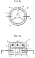
- Figure 1(a) shows a first embodiment of a holding device that employs spring loading. As shown in Figure 1(a), the configuration of microwave resonator 100 is maintained by holding device 25 .
- Holding device 25 includes sidewalls 45 , bottom plate 50 , top lid 60 , pressure plate 70 , and load springs 80 .
- Load springs 80 are sufficiently strong to retain the configuration of the microwave resonator during thermal cycling.
- Load springs 80 preferably are formed of nonmagnetic material in order to prevent disturbing the radio frequency fields in the resonator to achieve the highest possible Q-values.
- Load springs 80 preferably are formed of Be-Cu alloys.
- Parts 45 , 50 , 60 and 70 of holding device 25 are made of thermally and electrically conductive materials in order to reduce, radio frequency loss as well as to enable efficient cooling of resonator 100 .
- Parts 45 , 50 , 60 and 70 therefore may be formed of, for example, oxygen fired copper, aluminum, silver, preferably oxygen fired copper or aluminum.
- the high T c superconductor-dielectric microwave resonators of the invention are capable of attaining extremely high Q-values, due in part, to the ability of substrate 20 bearing film 10 to prevent axial radio frequency fields from extending beyond the London penetration depth of the superconducting film 10 . This is accomplished where substrates 20 are substantially greater than the diameter of dielectric 30 so that radio frequency fields are confined within the cavity region between substrates 20 .
- the high Q-value superconducting microwave resonators provided by the invention have a variety of potential applications. Typically, these resonators may be employed in applications such as filters, oscillators, as well as radio frequency energy storage devices.
- circuit 51 employs a microwave resonator 100 of the invention that is inserted into a closed feedback loop of, preferably, a low noise amplifier 15 .
- the product of the gain of amplifier 15 and the insertion loss of resonator 100 is greater than one, and where the total phase of the closed loop, as adjusted by phase shifter 17 , is a multiple of 2 ⁇ , then, due to the extremely high Q-values of the superconducting microwave resonators of the invention, the oscillator can be made to oscillate at the microwave resonator's resonant frequency to yield lower phase noise in the oscillator.
- the superconducting microwave resonators of the invention also may be employed to provide highly stable frequencies suitable for secondary standards for frequency or time. Since the microwave resonator has an extremely high Q-value and operates at a constant cryogenic temperature, the microwave resonator has a very stable resonate frequency that makes the resonator useful for serving as a secondary standard.
- the superconducting microwave resonators of the invention further may be employed as building blocks in passive devices such as filters. Examples of such filters are shown in Figures 3(a) and 3(b). As illustrated in Figure 3(a), filter 110 is shown in the form of a series of dielectrics 30 sandwiched between substrates 20 bearing superconducting films 10 . Coupling between dielectrics 30 is achieved by the evanescent fields of dielectrics 30 . Coupling of filter 10 to electronic circuits (not shown) can be achieved by coaxial cable 18 bearing coupling loop 21 .
- FIG. 3(b) shows an alternative embodiment of a filter.
- filter 120 employs a series of dielectrics 30 . Coupling between dielectrics 30 is achieved by the evanescent fields of dielectrics 30 via openings (not shown) on substrates 20 . Coupling of filter 120 to an electronic circuit (not shown) can be achieved by couplings 13 . Couplings 13 can be coaxial lines, waveguides, or other transmission lines. In either of the embodiments of Figures 3(a) or 3(b), the high Q-values of the superconducting microwave resonators reduces the in-band insertion loss of the filter so as to make the skirt of the frequency response curve of the filter steeper.
- high Q-values for the superconducting microwave resonators of the invention may be obtained by selecting the proper electromagnetic modes to prevent flow of radio frequency current across the edges of superconducting films 10 .
- the Q and the resonant frequency f 0 for the microwave resonator can be calculated by solving Maxwell's Equations for the boundary conditions of the resonator, as is known in the art.
- the loss power associated with parasitic coupling to low Q-value modes such as non-TE 0in modes or case modes may be minimized in the microwave resonators of the invention by assuring that substrates 20 are flat and parallel to within a tolerance of less than 1°. Loss power also may be minimized by ensuring that the C-axis of anisotropic materials such as sapphire, when employed as dielectric 30 , is perpendicular to substrate 20 to within ⁇ 5°, preferably 1°.
- microwave resonator 100 can be coupled to an electric circuit (not shown) by coaxial cable 18 that includes coupling loop 21 protruding into cavity 90 of microwave resonator 100 .
- coaxial cable 18 that includes coupling loop 21 protruding into cavity 90 of microwave resonator 100 .
- the orientation of coupling loop 21 and the depth of insertion of coaxial cable 18 into cavity 90 readily can be adjusted to ensure coupling to the electronic circuit.
- superconducting film is formed by epitaxially depositing 0.5 micron superconducting films of Tl 2 Ba 2 Ca 1 Cu 2 O or YBa 2 Cu 3 O on 2 inch diameter substrates of LaAlO 3 positioned on cylindrical dielectrics of sapphire.
- the superconducting film is deposited so that the C-axis of the film is perpendicular to the surface of the substrate.
- the dielectrics of sapphire typically measure 0.625 inch diameter by 0.276 inch tall, 0.625 inch diameter by 0.552 inch tall, or 1.00 inch diameter by 0.472 inch tall.
- the substrates and dielectric are retained in position by a holding device formed of oxygen free copper.
- Coupling of the microwave resonator to an electrical circuit can be achieved by inserting two 0.087 inch diameter copper or stainless steel, 50 ohm coaxial cables with coupling loops made of extended inner conductor into the cavity of the resonator.
- the Q values of the above described microwave resonators, when employing YBa 2 Cu 3 O as the superconducting film, are shown in Figure 4. As shown in Figure 4, Q values of 5 million, 1.5 million, and 0.25 million are found at temperatures of 4.2 K, 20 K and 50 K, respectively.
- the Q values of the above described microwave resonators, when employing Tl 2 Ba 2 Ca 1 Cu 2 O as the superconducting film, are shown in Figure 5. As shown in Figure 5, Q values of 6 million, 3 million, and 1.3 million are found at temperatures of 20 K, 50 K, and 77 K, respectively.
- Device 25 shown in Figure 1(a) that employs spring loading is only illustrative. Other means for holding microwave resonator 100 are shown below.
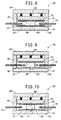
- FIGS 7(a) and 7(b) show an alternative embodiment for holding the microwave resonators of the invention.
- the microwave resonator is held by holding device 27 .
- Device 27 is indentical to device 25 except that, as shown in Figure 7(a), spring loaded holding device 27 employs three dielectric rods 35 positioned 120° relative to each other to further support dielectric 30 .
- Dielectric rods 35 are inserted through side walls 47 of holding device 27 into cavity 95 .
- Dielectric rods 35 have a low loss and a dielectric constant less than that of dielectric 30 .
- the tips of rods 35 are pointed to minimize contact area with dielectric 30 to minimize loss power.
- FIG. 8 A further embodiment of a device for holding the microwave resonators of the invention is shown in Figure 8. As set forth in Figure 8, the microwave resonator is retained in position by holding device 28 . Holding device 28 is identical to holding device 25 except for the additional use of retainer 77 . As shown in Figure 8, substrate 20 bearing superconducting film 10 is positioned on bottom-plate 50 . Dielectric 30 is positioned on substrate 20 . Retainer 77 is positioned about dielectric 30 . Retainer 77 contacts sidewalls 45 and superconducting film 10 on substrate 20 . Retainer 77 and side walls 45 have openings for receiving coaxial cables 18 . Cables 18 have loops 21 for coupling of the resonator to an electric circuit(not shown).
- Retainer 77 is formed of materials that have low dielectric constant of nearly 1 and low tan ⁇ of ⁇ 10 -4 . As shown in Figure 8, retainer 77 is hollow, and is solid near sidewalls 45 where the electrical fields are minimum. The wall thickness of retainer 77 is minimized to reduce the contact area between retainer 77 and dielectric 30 to minimize loss power.
- FIG. 9 Still yet another embodiment of a holder device for the microwave resonators of the invention is shown in Figure 9.
- Holding device 29 shown in Figure 9 is identical to holding device 25 except for the use of additional dielectric 65 .
- cavity 91 between dielectric 30 and the interior surface of sidewall 45 of device 25 is filled with dielectric material 65 .
- Dielectric material 65 has a tan ⁇ of less than 10 -5 . Examples of dielectric material 65 include styrofoam, porotic teflon, and the like.
- FIG 10 shows a further embodiment of a holding device suitable for use with the superconducting microwave resonators of the invention.
- Holding device 24 shown in Figure 10 is identical to holding device 25 except for additional use of holding pins 71 .
- pins 71 formed of low tan ⁇ dielectric materials such as sapphire, quartz, polymers, polytetrafluoroethylene ("teflon”), "Delrin", registered trademark of E. I. du Pont de Nemours and Company, and the like are inserted into substrate 20 bearing superconducting film 10 and into dielectric 30 .
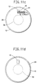
- FIG 11(a) shows a microstrip line coupling mechanism for coupling of the microwave resonators of the invention to an electronic circuit (not shown).
- microstrip line 15 is formed by depositing superconducting film material on that surface of substrate 20 that is remote to dielectric 30 .
- Microstrip line 15 serves as the lead to an electronic circuit (not shown).
- Opening 12 is provided in film 10 on the surface of substrate 20 that contacts dielectric 30 .
- Opening 12 extends through film 10 but not through substrate 20 .
- Opening 12 does not contact dielectric 30 in order to minimize the effects of magnetic fields on dielectric 30 .
- Opening 12 is parallel to the local magnetic field. Coupling is achieved by magnetic field leakage through opening 12 to line 15 .
- Microstrip line 15 extends over opening 12 by a distance of ⁇ /4, where ⁇ is the wavelength of the radio frequency field at the operating frequency of the resonator.
- Figure 11(b) shows a coplanar line coupling mechanism for coupling the microwave resonators of the invention to an electronic circuit (not shown).
- the coplanar line coupling is formed by depositing superconducting film material on that surface of substrate 20 that is remote to dielectric 30 to form center line 19 and ground plane 21 .
- the coplanar line coupling serves as the lead to an electronic circuit (not shown).
- the coplanar line coupling extends over opening 12 .
- Opening 12 is provided by film 10 on the surface of substrate 20 that contacts dielectric 30 . Opening 12 extends through film 10 but not through substrate 20 . Opening 12 does not contact dielectric 30 .
- center line 19 is short circuited to ground plane 21 .
- Center line 19 extends across opening 12 .
- Opening 12 is parallel to the local magnetic field. Coupling is achieved by magnetic field leakage through slot 12 to center line 19 .
- Figure 11(c) shows a parallel line coupling mechanism for coupling dielectric 30 to an electronic circuit (not shown).
- the parallel line coupling includes parallel lines 31 and loop 32 .
- the parallel line coupling is formed by depositing superconducting film material on that surface of substrate 20 that is remote to dielectric 30 .
- the parallel line coupling mechanism serves as the lead to an electronic circuit (not shown).
- Parallel lines 31 and loop 32 extend over opening 12 .
- Opening 12 is provided in film 10 on the surface of substrate 20 that contacts dielectric 30 . Opening 12 extends through film 10 but not through substract 20 . Opening 12 does not contact dielectric 30 . Coupling is achieved by leakage of magnetic field through opening 12 which is captured by loop 32 .
- Figure 11(d) shows a coupling mechanism useful for microwave resonators such as those used for a filter as shown in Figure 3(b).
- the coupling mechanism employs identical, congruent slots 12 through film 10 of both surfaces of substrate 20 . Slots 12 extend through films 10 but terminate at the surfaces of substrate 20 . Slots 12 on each surface of substrate 20 may be the same or different in size. Coupling is achieved by leakage of evanescent magnetic field through slots 12 .
- Coupling of the microwave resonator also may be achieved through dual couplings.
- Figure 12 shows a dual coupling mechanism that utilizes dual identical coupling microstrip lines 44(a) and 44(b) that cross slots 12(a) and 12(b) on film 10 .
- Slots 12(a) and 12(b) are provided in film 10 on that surface of the substrate 20 that contacts dielectric 30 .
- Slots 12(a) and 12(b) terminate at the surface of substrate 20 .
- Couplings 44(a) and 44(b) are connected by lead line 41 that is divided into equal length branches 42(a) and 42(b) . Lines 44(a) and 44(b) and lead line 41 are formed by depositing superconductive material onto substrate 20 .
- Coupling is achieved by leakage of evanescent magnetic field through slots 12(a) and 12(b) .
- the dual coupling mechanism shown in Figure 12 enables selective coupling to the TE 011 mode and suppresses competing electromagnetic field modes that have antisymmetrical magnetic field distribution.
- the coupling mechanisms of the invention also provide for ease of connection to circuits integrated onto substrate 20 .
- a circuit is integrated onto the side of substrate 20 that bears coupling mechanisms 55(a) and 55(b) .
- Couplings 55(a) and 55(b) may be formed by depositing superconductive film material onto substrate 20 over slots 12(a) and 12(b) .
- Slots 12(a) and 12(b) are provided in the superconducting film (not shown) on that side of substrate 20 that contacts dielectric 30 .
- Slots 12(a) and 12(b) extend through the superconductor film but terminate at the surface of substrate 20 . Coupling is achieved by leakage of magnetic field through slots 12(a) and 12(b) .
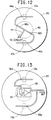
- circuits onto substrate 20 as shown in Figure 13 may be achieved by well known thin film printed circuit technology. If the circuit is a hybrid circuit that employs, for example, transistors, then the transistors can be integrated into the circuit by conventional wire bonding.
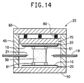
- Figure 14 shows an alternative embodiment of the superconducting microwave resonator of the invention that is retained by holding device 25 .
- rings 61 with a dielectric constant much less than that of dielectric 30 are inserted between dielectric 30 and superconducting film 10 . Rings 61 , by placing dielectric 30 further from superconducting film 10 , enable the microwave resonator to handle greater power levels.
Abstract
Description
- This invention relates to microwave resonators formed of high temperature superconductor and dielectric materials as well as to electronic circuits that employ those microwave resonators.
- Microwave resonators are known for use in time and frequency standards, frequency stable elements, as well as building blocks for passive devices such as filters and the like. The performance of the microwave resonator is gauged by its Q-value, expressed as
- Low temperature (Tc), such as 4 K, superconducting microwave resonators which employ a superconducting cavity made of Nb are known to have Q-values from about 106 to 109. (See V. B. Braginskii, et al: "The Properties of Superconducting Resonators on Sapphire", IEEE Trans. on Magn. Vol. 17, No. 1, P955, 1981, as a reference.) Although low Tc Nb microwave resonators have high Q-values, they must operate at very low temperatures (below 9 K). These microwave resonators require use of curved cavity walls. Curved cavity walls of materials which have a high Tc, of for example 77 K, however, are difficult to produce. On the other hand, high Q-value microwave resonators formed merely from a dielectric without an associated conducting medium also have high Q-values (see D. G. Blair, et al: "High Q Microwave Properties or a Sapphire Ring Resonator", J. Phys. D: Appl. Phys., 15, P1651, 1982.) However, the problems associated with the far reaching evanescent fields make them very bulky and vulnerable to microphonic effect, which limits the applications.
- Curtis, J. A. et al., 1991 IEEE MTT-5 International Microwave Symposium Digest, Vol. 2, pp. 447-450, June 10-14, 1991, Boston, MA, U.S. discloses hybrid dielectric/high temperature superconductor resonators and filter configurations using these resonators. For the TE011 mode resonators disclosed the Q-value is about 200,000 at 20 K. Pao, C. et al., 1988 IEEE MTT-S International Microwave Symposium Digest, Vol. 1, pp. 457-458, May 25-27, 1988, New York, NY, U.S. disclose a superconductor-dielectric resonator based on a sapphire tube loaded with two plates of Y-Ba-Cu oxides wherein a Q-factor of 105 to 106 may be achieved using a H01δ or H015 mode. Kogami, Y. et al., 1991 IEEE MTT-S International Microwave Symposium Digest, Vol. 3, pp. 1345-1348, June 10-14, 1991, Boston, MA, U.S. teaches a bandpass filter using two TM01δ mode dielectric rod resonators oriented axially in a high temperature superconductor cylinder having a Q value of 150,000 at 20 K. St. Martin, J. et al., Electronics Letters, Vol. 26, No. 24, November 22, 1990, pp. 2015-2016 discloses a dielectric resonator antenna consisting of a HEM11δ mode circular dielectric resonator fed by a microstrip feedline through a coupling aperture in the ground plant between them.
- The need therefore exists for microwave resonator made of high Tc , such as 77 K, superconductor that have Q-values comparable to low Tc superconducting microwave resonators made of Nb.
-
- Figures 1(a) and 1(b) show a vertical cross section of superconducting microwave resonator and a holding device for that resonator.
- Figure 2 is a schematic block diagram of a frequency stable element for oscillators that employs the microwave resonator of the invention.
- Figures 3(a) and 3(b) show configurations of filters using superconducting microwave resonators according to the invention.
- Figure 4 shows the Q-values of a superconducting microwave resonator of the invention that employ YBa2Cu3O superconductor and sapphire dielectric.
- Figure 5 shows the Q-values of a superconducting microwave resonator of the invention that employs TlBaCaCuO superconductor and sapphire dielectric.
- Figure 6 shows the relationship of Q-value or the resonator to the size of the dielectric.
- Figure 7 shows cross sectional views of an alternative embodiment of a device for holding the microwave resonators of the invention.
- Figure 8 shows a vertical cross section of a further embodiment of a device for holding the microwave resonator of the invention.
- Figure 9 shows a vertical cross section of a further alternative embodiment of a holding device for the microwave resonators of the invention.
- Figure 10 shows a vertical cross section of a further embodiment of a holding device for the microwave resonators of the invention.
- Figures 11(a)-11(d) show top views of alternative embodiments for coupling the microwave resonators of the invention to an electronic circuit.
- Figure 12 shows a top view of a coupling mechanism that utilizes dual couplings for coupling the microwave resonators of the invention to an electronic circuit.
- Figure 13 shows a top view of a coupling of the microwave resonator of the invention to an electronic circuit integrated onto the back side of the substrate.
- Figure 14 shows a vertical cross section of an alternative embodiment of the microwave resonators of the invention.
-
- The invention is directed to high temperature superconductor-dielectric microwave resonators, to holding devices for those resonators, coupling of those resonators to electronic circuits, and to their methods of manufacture. The superconducting microwave resonator of the invention employ a superconducting film on substrates positioned on a dielectric. The holding devices include a variety of configurations, such as, a spring loaded device. The microwave resonators can be readily coupled to electronic circuits. The superconducting microwave resonators have Q values that are as high as low temperature microwave resonators formed of Nb, but operate at much higher temperature.
- In accordance with a first aspect of the present invention there is provided a high temperature superconducting microwave resonator as defined in claim 1.
- In accordance with a further aspect of the present invention there is provided a method for coupling to an electric circuit such a superconducting microwave resonator, as defined in claim 17.
- Having briefly summarized the invention, the invention will now be described in detail by reference to the following description and non-limiting examples. Unless otherwise specified, all percentages are by weight and all temperatures are in degrees Kelvin.
- Figure 1 shows superconducting microwave resonator and a holding device for that resonator. As shown in Figures 1(a) and 1(b), a superconducting microwave resonator 100 with cavity 90 is provided in the form of substrates 20 bearing superconducting film 10 positioned on dielectric 30. Substrate 20 is a single crystal that has a lattice matched to superconductor film 10. Preferably, substrates 20 are formed of LaAlO3, NdGaO3, MgO and the like.
- Generally, superconductor film 10 may be formed from any high Tc superconducting material that has a surface resistance (Rs) that is at least ten times less than that of copper at any specific operating temperature. Tc can be determined by the "eddy current method" using a LakeShore Superconductor Screening System, Model No. 7500. Surface resistance of superconducting film 10 can be measured by the method described in Wilker et al., "5-GHz High-Temperature-Superconductor Resonators with High Q and Low Power Dependence up to 90 K", IEEE, Trans. on Microwave Theory and Techniques, Vol. 39, No. 9, September 1991, pp. 1462-1467. Generally, superconductor film 10 is formed from materials such as YBaCuO (123), TlBaCaCuO (2212 or 2223), TlPbSrCaCuO (1212 or 1223), or the like.
- Superconducting film 10 can be deposited onto substrate 20 by methods known in the art. See, for example, Holstein et al., "Preparation and Characterization of Tl2Ba2CaCu2O8 Films on 100 LaAlO3", IEEE, Trans. Magn., Vol. 27, pp. 1568-1572, 1991 and Laubacher et al., "Processing and Yield of YBa2Cu3O7-x Thin Films and Devices Produced with a BaF2 Process", IEEE, Trans. Magn., Vol. 27, pp. 1418-1421, 1991. Generally, the thickness of film 10 is in the range of 0.2 to 1.0 micron, preferably 0.5 to 0.8 micron.
- Microwave resonator 100 is formed by positioning substrates 20 bearing superconducting film 10 on dielectric 30. Substrates 20 can be placed on the surface of dielectric 30, or, alternatively, low loss adhesive materials may be employed. Polymethyl methacrylate optionally may be deposited onto the surface of superconducting film 10 to more firmly bond dielectric 30, as well as to protect superconducting film 10.
- Dielectric 30 may be provided in a variety of shapes. Preferably, dielectric 30 is in the form of circular cylinders or polygons. Dielectric 30 may be formed of any dielectric material with a dielectric constant εr>1. Such dielectric materials include, for example, sapphire, fused quartz, and the like. Generally, these dielectric materials have a loss factor (
- The configuration of the microwave resonator 100, when in use, is maintained by holding device 25. The holding device can be any embodiment that maintains the relative positions of the components of the resonator during thermal cycling associated with use of the resonator. Figure 1(a) shows a first embodiment of a holding device that employs spring loading. As shown in Figure 1(a), the configuration of microwave resonator 100 is maintained by holding device 25. Holding device 25 includes sidewalls 45, bottom plate 50, top lid 60, pressure plate 70, and load springs 80. Load springs 80 are sufficiently strong to retain the configuration of the microwave resonator during thermal cycling. Load springs 80 preferably are formed of nonmagnetic material in order to prevent disturbing the radio frequency fields in the resonator to achieve the highest possible Q-values. Load springs 80 preferably are formed of Be-Cu alloys.
- Parts 45, 50, 60 and 70 of holding device 25 are made of thermally and electrically conductive materials in order to reduce, radio frequency loss as well as to enable efficient cooling of resonator 100. Parts 45, 50, 60 and 70 therefore may be formed of, for example, oxygen fired copper, aluminum, silver, preferably oxygen fired copper or aluminum.
- The high Tc superconductor-dielectric microwave resonators of the invention are capable of attaining extremely high Q-values, due in part, to the ability of substrate 20 bearing film 10 to prevent axial radio frequency fields from extending beyond the London penetration depth of the superconducting film 10. This is accomplished where substrates 20 are substantially greater than the diameter of dielectric 30 so that radio frequency fields are confined within the cavity region between substrates 20.
- The high Q-value superconducting microwave resonators provided by the invention have a variety of potential applications. Typically, these resonators may be employed in applications such as filters, oscillators, as well as radio frequency energy storage devices.
- The microwave resonators of the invention also may be employed as frequency stable elements to reduce the phase noise for oscillators. As shown in Figure 2, circuit 51 employs a microwave resonator 100 of the invention that is inserted into a closed feedback loop of, preferably, a low noise amplifier 15. Where the product of the gain of amplifier 15 and the insertion loss of resonator 100 is greater than one, and where the total phase of the closed loop, as adjusted by phase shifter 17, is a multiple of 2π, then, due to the extremely high Q-values of the superconducting microwave resonators of the invention, the oscillator can be made to oscillate at the microwave resonator's resonant frequency to yield lower phase noise in the oscillator.
- The superconducting microwave resonators of the invention also may be employed to provide highly stable frequencies suitable for secondary standards for frequency or time. Since the microwave resonator has an extremely high Q-value and operates at a constant cryogenic temperature, the microwave resonator has a very stable resonate frequency that makes the resonator useful for serving as a secondary standard.
- The superconducting microwave resonators of the invention further may be employed as building blocks in passive devices such as filters. Examples of such filters are shown in Figures 3(a) and 3(b). As illustrated in Figure 3(a), filter 110 is shown in the form of a series of dielectrics 30 sandwiched between substrates 20 bearing superconducting films 10. Coupling between dielectrics 30 is achieved by the evanescent fields of dielectrics 30. Coupling of filter 10 to electronic circuits (not shown) can be achieved by coaxial cable 18 bearing coupling loop 21.
- Figure 3(b) shows an alternative embodiment of a filter. As shown in Figure 3(b), filter 120 employs a series of dielectrics 30. Coupling between dielectrics 30 is achieved by the evanescent fields of dielectrics 30 via openings (not shown) on substrates 20. Coupling of filter 120 to an electronic circuit (not shown) can be achieved by couplings 13. Couplings 13 can be coaxial lines, waveguides, or other transmission lines. In either of the embodiments of Figures 3(a) or 3(b), the high Q-values of the superconducting microwave resonators reduces the in-band insertion loss of the filter so as to make the skirt of the frequency response curve of the filter steeper.
- An additional application of the superconducting, microwave resonators of the invention is to measure the surface impedance (Zs) of superconductor materials and the complex dielectric constant
- Generally, high Q-values for the superconducting microwave resonators of the invention may be obtained by selecting the proper electromagnetic modes to prevent flow of radio frequency current across the edges of superconducting films 10. These proper modes are TEoin modes where the radial mode index has a value of i=1,2,3,... and the axial mode index has a value of n=1,2,3,... All TEoin modes have only circular radio frequency currents that do not cross the edge of films 10.
- Having selected the specific electromagnetic mode of the microwave resonator, the Q and the resonant frequency f0 for the microwave resonator can be calculated by solving Maxwell's Equations for the boundary conditions of the resonator, as is known in the art.
- The loss power associated with parasitic coupling to low Q-value modes such as non-TE0in modes or case modes may be minimized in the microwave resonators of the invention by assuring that substrates 20 are flat and parallel to within a tolerance of less than 1°. Loss power also may be minimized by ensuring that the C-axis of anisotropic materials such as sapphire, when employed as dielectric 30, is perpendicular to substrate 20 to within ± 5°, preferably 1°.
- As also is shown in Figure 1(a), microwave resonator 100 can be coupled to an electric circuit (not shown) by coaxial cable 18 that includes coupling loop 21 protruding into cavity 90 of microwave resonator 100. The orientation of coupling loop 21 and the depth of insertion of coaxial cable 18 into cavity 90 readily can be adjusted to ensure coupling to the electronic circuit.
- In a preferred aspect of the invention, superconducting film is formed by epitaxially depositing 0.5 micron superconducting films of Tl2Ba2Ca1Cu2O or YBa2Cu3O on 2 inch diameter substrates of LaAlO3 positioned on cylindrical dielectrics of sapphire. The superconducting film is deposited so that the C-axis of the film is perpendicular to the surface of the substrate. The dielectrics of sapphire typically measure 0.625 inch diameter by 0.276 inch tall, 0.625 inch diameter by 0.552 inch tall, or 1.00 inch diameter by 0.472 inch tall. The substrates and dielectric are retained in position by a holding device formed of oxygen free copper. Coupling of the microwave resonator to an electrical circuit can be achieved by inserting two 0.087 inch diameter copper or stainless steel, 50 ohm coaxial cables with coupling loops made of extended inner conductor into the cavity of the resonator. The surface of the coupling loops is perpendicular to the vertical axis of the sapphire dielectric to enable selective coupling to the TE011 (i=1, n=1) mode of the dielectric.
- The Q values of the above described microwave resonators, when employing YBa2Cu3O as the superconducting film, are shown in Figure 4. As shown in Figure 4, Q values of 5 million, 1.5 million, and 0.25 million are found at temperatures of 4.2 K, 20 K and 50 K, respectively. The Q values of the above described microwave resonators, when employing Tl2Ba2Ca1Cu2O as the superconducting film, are shown in Figure 5. As shown in Figure 5, Q values of 6 million, 3 million, and 1.3 million are found at temperatures of 20 K, 50 K, and 77 K, respectively.
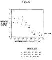
- The dependence of Q values of the above described microwave resonators that employ Tl2Ba2Ca1Cu2O as the superconducting film on the size of the sapphire dielectric is shown in Figure 6. As shown in Figure 6, the Q values increase from 3 million to 6 million with increasing size of the sapphire dielectric.
- Device 25 shown in Figure 1(a) that employs spring loading is only illustrative. Other means for holding microwave resonator 100 are shown below.
- Figures 7(a) and 7(b) show an alternative embodiment for holding the microwave resonators of the invention. As shown in Figure 7, the microwave resonator is held by holding device 27. Device 27 is indentical to device 25 except that, as shown in Figure 7(a), spring loaded holding device 27 employs three dielectric rods 35 positioned 120° relative to each other to further support dielectric 30. Dielectric rods 35 are inserted through side walls 47 of holding device 27 into cavity 95. Dielectric rods 35 have a low loss and a dielectric constant less than that of dielectric 30. The tips of rods 35 are pointed to minimize contact area with dielectric 30 to minimize loss power.
- A further embodiment of a device for holding the microwave resonators of the invention is shown in Figure 8. As set forth in Figure 8, the microwave resonator is retained in position by holding device 28. Holding device 28 is identical to holding device 25 except for the additional use of retainer 77. As shown in Figure 8, substrate 20 bearing superconducting film 10 is positioned on bottom-plate 50. Dielectric 30 is positioned on substrate 20. Retainer 77 is positioned about dielectric 30. Retainer 77 contacts sidewalls 45 and superconducting film 10 on substrate 20. Retainer 77 and side walls 45 have openings for receiving coaxial cables 18. Cables 18 have loops 21 for coupling of the resonator to an electric circuit(not shown). Retainer 77 is formed of materials that have low dielectric constant of nearly 1 and low
- Still yet another embodiment of a holder device for the microwave resonators of the invention is shown in Figure 9. Holding device 29 shown in Figure 9 is identical to holding device 25 except for the use of additional dielectric 65. As shown in Figure 9, cavity 91 between dielectric 30 and the interior surface of sidewall 45 of device 25 is filled with dielectric material 65. Dielectric material 65 has a
- Figure 10 shows a further embodiment of a holding device suitable for use with the superconducting microwave resonators of the invention. Holding device 24 shown in Figure 10 is identical to holding device 25 except for additional use of holding pins 71. As shown in Figure 10, pins 71, formed of low
- Figures 11(a) to 11(d) show alternative embodiments for coupling of the microwave resonators of the invention to an electronic circuit (not shown). Generally, the embodiments shown in Figures 11(a)-11(c) entail use of substrates that bear superconducting films on the surfaces of the substrate that directly contacts dielectric 30. Openings are provided on the superconducting film on the side which directly contacts dielectric 30. A coupling device is located over the opening on surface of the substrate that does not contact dielectric 30.
- Figure 11(a) shows a microstrip line coupling mechanism for coupling of the microwave resonators of the invention to an electronic circuit (not shown). In Figure 11(a), microstrip line 15 is formed by depositing superconducting film material on that surface of substrate 20 that is remote to dielectric 30. Microstrip line 15 serves as the lead to an electronic circuit (not shown). Opening 12 is provided in film 10 on the surface of substrate 20 that contacts dielectric 30. Opening 12 extends through film 10 but not through substrate 20. Opening 12 does not contact dielectric 30 in order to minimize the effects of magnetic fields on dielectric 30. Opening 12 is parallel to the local magnetic field. Coupling is achieved by magnetic field leakage through opening 12 to line 15. Microstrip line 15 extends over opening 12 by a distance of λ/4, where λ is the wavelength of the radio frequency field at the operating frequency of the resonator.
- Figure 11(b) shows a coplanar line coupling mechanism for coupling the microwave resonators of the invention to an electronic circuit (not shown). The coplanar line coupling is formed by depositing superconducting film material on that surface of substrate 20 that is remote to dielectric 30 to form center line 19 and ground plane 21. The coplanar line coupling serves as the lead to an electronic circuit (not shown). The coplanar line coupling extends over opening 12. Opening 12 is provided by film 10 on the surface of substrate 20 that contacts dielectric 30. Opening 12 extends through film 10 but not through substrate 20. Opening 12 does not contact dielectric 30.
- In the coplanar line coupling of Figure 11(b), center line 19 is short circuited to ground plane 21. Center line 19 extends across opening 12. Opening 12 is parallel to the local magnetic field. Coupling is achieved by magnetic field leakage through slot 12 to center line 19.
- Figure 11(c) shows a parallel line coupling mechanism for coupling dielectric 30 to an electronic circuit (not shown). The parallel line coupling includes parallel lines 31 and loop 32. The parallel line coupling is formed by depositing superconducting film material on that surface of substrate 20 that is remote to dielectric 30. The parallel line coupling mechanism serves as the lead to an electronic circuit (not shown). Parallel lines 31 and loop 32 extend over opening 12. Opening 12 is provided in film 10 on the surface of substrate 20 that contacts dielectric 30. Opening 12 extends through film 10 but not through substract 20. Opening 12 does not contact dielectric 30. Coupling is achieved by leakage of magnetic field through opening 12 which is captured by loop 32.
- Figure 11(d) shows a coupling mechanism useful for microwave resonators such as those used for a filter as shown in Figure 3(b). As shown in Figure 11(d), the coupling mechanism employs identical, congruent slots 12 through film 10 of both surfaces of substrate 20. Slots 12 extend through films 10 but terminate at the surfaces of substrate 20. Slots 12 on each surface of substrate 20 may be the same or different in size. Coupling is achieved by leakage of evanescent magnetic field through slots 12.
- Coupling of the microwave resonator also may be achieved through dual couplings. Figure 12 shows a dual coupling mechanism that utilizes dual identical coupling microstrip lines 44(a) and 44(b) that cross slots 12(a) and 12(b) on film 10. Slots 12(a) and 12(b) are provided in film 10 on that surface of the substrate 20 that contacts dielectric 30. Slots 12(a) and 12(b) terminate at the surface of substrate 20. Couplings 44(a) and 44(b) are connected by lead line 41 that is divided into equal length branches 42(a) and 42(b). Lines 44(a) and 44(b) and lead line 41 are formed by depositing superconductive material onto substrate 20. Coupling is achieved by leakage of evanescent magnetic field through slots 12(a) and 12(b). The dual coupling mechanism shown in Figure 12 enables selective coupling to the TE011 mode and suppresses competing electromagnetic field modes that have antisymmetrical magnetic field distribution.
- The coupling mechanisms of the invention also provide for ease of connection to circuits integrated onto substrate 20. As shown in Figure 13, a circuit is integrated onto the side of substrate 20 that bears coupling mechanisms 55(a) and 55(b). Couplings 55(a) and 55(b) may be formed by depositing superconductive film material onto substrate 20 over slots 12(a) and 12(b). Slots 12(a) and 12(b) are provided in the superconducting film (not shown) on that side of substrate 20 that contacts dielectric 30. Slots 12(a) and 12(b) extend through the superconductor film but terminate at the surface of substrate 20. Coupling is achieved by leakage of magnetic field through slots 12(a) and 12(b).
- Integration of circuits onto substrate 20 as shown in Figure 13 may be achieved by well known thin film printed circuit technology. If the circuit is a hybrid circuit that employs, for example, transistors, then the transistors can be integrated into the circuit by conventional wire bonding.
- Figure 14 shows an alternative embodiment of the superconducting microwave resonator of the invention that is retained by holding device 25. As shown in Figure 14, rings 61 with a dielectric constant much less than that of dielectric 30 are inserted between dielectric 30 and superconducting film 10. Rings 61, by placing dielectric 30 further from superconducting film 10, enable the microwave resonator to handle greater power levels.
Claims (18)
- A high temperature superconducting microwave resonator (100) operating in the TE0in mode, where i and n are integers of at least 1, the resonator (100) comprising a dielectric (30) and a plurality of substrates (20) bearing a coating of high temperature superconducting material (10), wherein said substrates are positioned relative to said dielectric to enable said coating to contact said dielectric, characterised in that said dielectric has a loss factor (
- The high temperature superconducting microwave resonator of Claim 1 wherein said dielectric (30) is selected from sapphire and quartz.
- The high temperature superconducting microwave resonator of Claim 2 wherein said dielectric (30) is sapphire.
- The high temperature superconducting microwave resonator of any preceding claim wherein said substrates (20) are single crystals that are lattice matched to said superconducting material.
- The high temperature superconducting microwave resonator of Claim 4 wherein said substrates (20) are selected from LaAlO3, NdGaO3 and MgO.
- The high temperature superconducting microwave resonator of any preceding claim 1 wherein said superconducting material (10) has a surface resistance at least ten times less than copper.
- The high temperature superconducting microwave resonator of Claim 6 wherein said superconducting material (10) is selected from YBaCuO (123), T1BaCaCuO (2212), T1BaCaCuO (2223), T1PbSrCaCuO (1212) or T1PbSrCaCuO (1223).
- The resonator of any preceding claim, wherein said holding device (25) is formed of conductive materials selected from copper, aluminium and silver.
- The resonator of any preceding claim, wherein springs (80) formed of non-magnetic material are positioned between and in contact with the device top (60) and the said plate (70).
- The high temperature superconducting microwave resonator of any preceding claim, further comprising dielectric rings (61) positioned between said dielectric (30) and said substrate (20).
- The resonator of any one of claims 1 to 9, wherein said holding device (25) further comprises a plurality of spaced dielectric rods (35) positioned to contact the dielectric (30) of said resonator (100) and maintain said dielectric (30) in position relative to the sidewalls (45) of said device (25), wherein the rods (35) comprise a dielectric material that is different from the dielectric material of the dielectric element (30) of said resonator (100).
- The resonator of any one of claims 1 to 9, wherein said holding device (25) includes an additional dielectric material (65) between said substrate and said dielectric of said microwave resonator, wherein said dielectric material is different from said dielectric of said microwave resonator.
- The resonator of any one of claims 1 to 9, wherein said holding device (25) further comprises a retainer (77) positioned between said substrates and contacting said dielectric.
- The resonator of any preceding claim, further comprising a coupling means for transferring electromagnetic energy between said dielectric to an electrical circuit.
- The resonator of Claim 14, wherein said coupling means comprises a coaxial cable (18) with coupling loops formed of extended inner conductor of said cable, said cable being positioned between said substrates (20) of said microwave resonator.
- A microwave filter comprising a high temperature superconducting microwave resonator as defined in any preceding claim, wherein said dielectric (30) comprises a plurality of resonant dielectric elements (30) each of which is positioned between a respective pair of said substrates (20) and in contact with said superconducting material (10), said filter further comprising coupling means (13; 18,21) connected to at least one of said resonant dielectric elements (30) and to an electronic circuit.
- A method for coupling to an electric circuit a superconducting microwave resonator according to Claim 1, wherein the substrates of the resonator have at least one opening (12) therein for passing electromagnetic fields generated by said dielectric, which method comprises employing a means positioned on said substrate for transferring said electromagnetic fields passing through said opening to an electrical circuit.
- The method of Claim 17, wherein said means is a microstrip line, coplanar line or parallel line.
Applications Claiming Priority (3)
| Application Number | Priority Date | Filing Date | Title |
|---|---|---|---|
| US07/788,063 US5324713A (en) | 1991-11-05 | 1991-11-05 | High temperature superconductor support structures for dielectric resonator |
| US788063 | 1991-11-05 | ||
| PCT/US1992/009635 WO1993009575A1 (en) | 1991-11-05 | 1992-11-05 | High-temperature superconductor-dielectric resonator |
Publications (2)
| Publication Number | Publication Date |
|---|---|
| EP0611489A1 EP0611489A1 (en) | 1994-08-24 |
| EP0611489B1 true EP0611489B1 (en) | 2000-05-03 |
Family
ID=25143338
Family Applications (1)
| Application Number | Title | Priority Date | Filing Date |
|---|---|---|---|
| EP92924372A Expired - Lifetime EP0611489B1 (en) | 1991-11-05 | 1992-11-05 | High-temperature superconductor-dielectric resonator |
Country Status (14)
| Country | Link |
|---|---|
| US (1) | US5324713A (en) |
| EP (1) | EP0611489B1 (en) |
| JP (1) | JP3463933B2 (en) |
| KR (2) | KR940703084A (en) |
| AT (1) | ATE192607T1 (en) |
| AU (1) | AU3070292A (en) |
| CA (1) | CA2122605C (en) |
| DE (1) | DE69231000T2 (en) |
| DK (1) | DK0611489T3 (en) |
| ES (1) | ES2148182T3 (en) |
| GR (1) | GR3033562T3 (en) |
| HK (1) | HK1003756A1 (en) |
| SG (1) | SG63630A1 (en) |
| WO (1) | WO1993009575A1 (en) |
Families Citing this family (33)
| Publication number | Priority date | Publication date | Assignee | Title |
|---|---|---|---|---|
| ES2092836T3 (en) * | 1992-08-21 | 1996-12-01 | Du Pont | APPARATUS FOR CHARACTERIZING THIN SUPERCONDUCTING FILMS AT HIGH TEMPERATURE. |
| WO1994028592A1 (en) * | 1993-05-27 | 1994-12-08 | E.I. Du Pont De Nemours And Company | High tc superconductor/ferroelectric tunable microwave circuits |
| US5585331A (en) * | 1993-12-03 | 1996-12-17 | Com Dev Ltd. | Miniaturized superconducting dielectric resonator filters and method of operation thereof |
| KR100389525B1 (en) * | 1994-06-03 | 2003-08-19 | 이.아이,듀우판드네모아앤드캄파니 | Fluoropolymer protectant layer for high temperature superconductor film and photo-definition thereof |
| US5759625A (en) * | 1994-06-03 | 1998-06-02 | E. I. Du Pont De Nemours And Company | Fluoropolymer protectant layer for high temperature superconductor film and photo-definition thereof |
| US5532210A (en) * | 1994-06-08 | 1996-07-02 | E. I. Du Pont De Nemours And Company | High temperature superconductor dielectric slow wave structures for accelerators and traveling wave tubes |
| GB9415923D0 (en) * | 1994-08-04 | 1994-09-28 | Secretary Trade Ind Brit | Method of and apparatus for calibration |
| US5616540A (en) * | 1994-12-02 | 1997-04-01 | Illinois Superconductor Corporation | Electromagnetic resonant filter comprising cylindrically curved split ring resonators |
| US5629266A (en) * | 1994-12-02 | 1997-05-13 | Lucent Technologies Inc. | Electromagnetic resonator comprised of annular resonant bodies disposed between confinement plates |
| GB9426294D0 (en) * | 1994-12-28 | 1995-02-22 | Mansour Raafat | High power soperconductive circuits and method of construction thereof |
| DE19524633A1 (en) * | 1995-07-06 | 1997-01-09 | Bosch Gmbh Robert | Waveguide resonator arrangement and use |
| GB2307355A (en) * | 1995-11-17 | 1997-05-21 | Pyronix Ltd | Dielectric resonator |
| US6083883A (en) * | 1996-04-26 | 2000-07-04 | Illinois Superconductor Corporation | Method of forming a dielectric and superconductor resonant structure |
| DE19617698C1 (en) * | 1996-05-03 | 1997-10-16 | Forschungszentrum Juelich Gmbh | Dual-mode two-pole filter |
| JP3331949B2 (en) * | 1998-02-20 | 2002-10-07 | 株式会社村田製作所 | Dielectric filter, dielectric duplexer and communication device |
| US6711394B2 (en) | 1998-08-06 | 2004-03-23 | Isco International, Inc. | RF receiver having cascaded filters and an intermediate amplifier stage |
| US6314309B1 (en) | 1998-09-22 | 2001-11-06 | Illinois Superconductor Corp. | Dual operation mode all temperature filter using superconducting resonators |
| WO2002058185A1 (en) * | 2001-01-19 | 2002-07-25 | Matsushita Electric Industrial Co., Ltd. | High frequency circuit element and high frequency circuit module |
| EP1527497A1 (en) * | 2002-04-10 | 2005-05-04 | South Bank University Enterprises Ltd. | Tuneable dielectric resonator |
| US20040021535A1 (en) * | 2002-07-31 | 2004-02-05 | Kenneth Buer | Automated dielectric resonator placement and attachment method and apparatus |
| US6894584B2 (en) | 2002-08-12 | 2005-05-17 | Isco International, Inc. | Thin film resonators |
| CN100466375C (en) * | 2005-01-21 | 2009-03-04 | 南京大学 | Composite resonant cavity for measuring microwave surface resistance of conductive material |
| KR100775859B1 (en) | 2005-03-31 | 2007-11-13 | 건국대학교 산학협력단 | Method for measuring the intrinsic surface impedance of superconducting materials in the microwave region |
| JP4711988B2 (en) * | 2007-03-15 | 2011-06-29 | 富士通株式会社 | Superconducting disk resonator, manufacturing method thereof, and evaluation method of dielectric anisotropy |
| WO2009027719A1 (en) * | 2007-08-31 | 2009-03-05 | Bae Systems Plc | Low vibration dielectric resonant oscillators |
| US20100171572A1 (en) * | 2007-08-31 | 2010-07-08 | Bae Systems Plc | Low vibration dielectric resonant oscillators |
| WO2009027721A1 (en) * | 2007-08-31 | 2009-03-05 | Bae Systems Plc | Low vibration dielecrick resonant oscillators |
| JP5115314B2 (en) * | 2008-05-08 | 2013-01-09 | 富士通株式会社 | Three-dimensional filter and tunable filter device |
| DE102009005468B4 (en) * | 2009-01-21 | 2019-03-28 | Rohde & Schwarz Gmbh & Co. Kg | Method and device for determining the microwave surface resistance |
| US8954125B2 (en) | 2011-07-28 | 2015-02-10 | International Business Machines Corporation | Low-loss superconducting devices |
| CN110089026B (en) * | 2016-12-22 | 2023-06-09 | 楼氏卡泽诺维亚公司 | Stable oscillator of microwave cavity resonator and implementation method thereof |
| RU192872U1 (en) * | 2019-05-31 | 2019-10-03 | Федеральное государственное автономное образовательное учреждение высшего образования "Санкт-Петербургский государственный университет аэрокосмического приборостроения" | THERMOSTABLE RESONATOR |
| CN116683262B (en) * | 2023-08-02 | 2023-11-03 | 苏州浪潮智能科技有限公司 | Microwave source, manufacturing method thereof and microwave laser generating method |
Family Cites Families (11)
| Publication number | Priority date | Publication date | Assignee | Title |
|---|---|---|---|---|
| FR2431773A1 (en) * | 1978-07-21 | 1980-02-15 | Thomson Csf | MICROWAVE FILTER WITH DIELECTRIC RESONATORS AND TELECOMMUNICATIONS EQUIPMENT PROVIDED WITH SUCH A FILTER |
| JPS63250201A (en) * | 1987-04-06 | 1988-10-18 | Murata Mfg Co Ltd | Dielectric resonator |
| JPS63266902A (en) * | 1987-04-23 | 1988-11-04 | Murata Mfg Co Ltd | Dielectric resonator |
| JPS63284902A (en) * | 1987-05-15 | 1988-11-22 | Murata Mfg Co Ltd | Dielectric resonator |
| JPH0691363B2 (en) * | 1987-05-29 | 1994-11-14 | 株式会社村田製作所 | Dielectric resonator device and cavity resonator device |
| FR2616594B1 (en) * | 1987-06-09 | 1989-07-07 | Thomson Csf | TUNABLE MICROWAVE FILTER DEVICE WITH DIELECTRIC RESONATOR, AND APPLICATIONS |
| JPS6420902A (en) * | 1987-07-17 | 1989-01-24 | Mazda Motor | Generating device |
| JPS6444104A (en) * | 1987-08-12 | 1989-02-16 | Nippon Telegraph & Telephone | Superconduction cavity resonator and its manufacture |
| US4963841A (en) * | 1989-05-25 | 1990-10-16 | Raytheon Company | Dielectric resonator filter |
| US5034711A (en) * | 1990-01-23 | 1991-07-23 | Hughes Aircraft Company | Dielectric resonator support system for a waveguide |
| US5179074A (en) * | 1991-01-24 | 1993-01-12 | Space Systems/Loral, Inc. | Hybrid dielectric resonator/high temperature superconductor filter |
-
1991
- 1991-11-05 US US07/788,063 patent/US5324713A/en not_active Expired - Fee Related
-
1992
- 1992-11-05 AU AU30702/92A patent/AU3070292A/en not_active Abandoned
- 1992-11-05 SG SG1996008241A patent/SG63630A1/en unknown
- 1992-11-05 DE DE69231000T patent/DE69231000T2/en not_active Expired - Fee Related
- 1992-11-05 AT AT92924372T patent/ATE192607T1/en not_active IP Right Cessation
- 1992-11-05 EP EP92924372A patent/EP0611489B1/en not_active Expired - Lifetime
- 1992-11-05 KR KR1019940701488A patent/KR940703084A/en not_active IP Right Cessation
- 1992-11-05 DK DK92924372T patent/DK0611489T3/en active
- 1992-11-05 CA CA002122605A patent/CA2122605C/en not_active Expired - Fee Related
- 1992-11-05 JP JP50877293A patent/JP3463933B2/en not_active Expired - Fee Related
- 1992-11-05 ES ES92924372T patent/ES2148182T3/en not_active Expired - Lifetime
- 1992-11-05 WO PCT/US1992/009635 patent/WO1993009575A1/en active IP Right Grant
-
1994
- 1994-05-04 KR KR940701488A patent/KR100300284B1/ko active
-
1998
- 1998-04-01 HK HK98102744A patent/HK1003756A1/en not_active IP Right Cessation
-
2000
- 2000-05-31 GR GR20000401255T patent/GR3033562T3/en not_active IP Right Cessation
Also Published As
| Publication number | Publication date |
|---|---|
| GR3033562T3 (en) | 2000-09-29 |
| EP0611489A1 (en) | 1994-08-24 |
| DK0611489T3 (en) | 2000-08-07 |
| WO1993009575A1 (en) | 1993-05-13 |
| JP3463933B2 (en) | 2003-11-05 |
| US5324713A (en) | 1994-06-28 |
| KR940703084A (en) | 1994-09-17 |
| KR100300284B1 (en) | 2001-10-22 |
| DE69231000D1 (en) | 2000-06-08 |
| ES2148182T3 (en) | 2000-10-16 |
| DE69231000T2 (en) | 2000-11-09 |
| HK1003756A1 (en) | 1998-11-06 |
| AU3070292A (en) | 1993-06-07 |
| CA2122605C (en) | 2002-10-08 |
| ATE192607T1 (en) | 2000-05-15 |
| CA2122605A1 (en) | 1993-05-13 |
| JPH07500956A (en) | 1995-01-26 |
| SG63630A1 (en) | 1999-03-30 |
Similar Documents
| Publication | Publication Date | Title |
|---|---|---|
| EP0611489B1 (en) | High-temperature superconductor-dielectric resonator | |
| Wilker et al. | A sapphire resonator for microwave characterization of superconducting thin films | |
| Krupka et al. | Measurements of permittivity, dielectric loss tangent, and resistivity of float-zone silicon at microwave frequencies | |
| Gallop | Microwave applications of high-temperature superconductors | |
| Cherpak et al. | Accurate microwave technique of surface resistance measurement of large-area HTS films using sapphire quasi-optical resonator | |
| JPH11507786A (en) | Tunable microwave device | |
| Anlage et al. | A current controlled variable delay superconducting transmission line | |
| Oates et al. | Tunable YBCO resonators on YIG substrates | |
| Hein | Progress, properties and prospects of passive high-temperature superconductive microwave devices in Europe | |
| Ginefri et al. | Comparison of radio-frequency and microwave superconducting properties of YBaCuO dedicated to magnetic resonance imaging | |
| Shanehsazzadeh et al. | Integrated Monolayer Planar Flux Transformer and Resonator Tank Circuit for High-$ T_ {c} $ RF-SQUID Magnetometer | |
| Oates et al. | Superconductor ferrite phase shifters and circulators | |
| Klein et al. | YBCO shielded LaAlO/sub 3/dielectric resonators for stable oscillators | |
| Zhang et al. | In-situ electron paramagnetic resonance studies of paramagnetic point defects in superconducting microwave resonators | |
| Oates | Microwave resonators and filters | |
| Mage et al. | Advances in the application of high Tc superconductors to microwave devices for analog signal processing | |
| Saito et al. | Dependence of surface resistance in HTS thin films on a DC magnetic field | |
| Hedges et al. | An extracted pole microstrip elliptic function filter using high temperature superconductors | |
| Yoshida et al. | Residual surface resistance of YBa/sub 2/Cu/sub 3/O/sub x/thin films-weakly coupled grain model | |
| Misra et al. | Laterally resolved microwave surface-resistance measurement of high-T/sub c/superconductor samples by cavity substitution technique | |
| Huang et al. | Dielectric waveguide resonator with a superconductive boundary layer | |
| Manzel et al. | High Q-value resonators for the SHF-region based on TBCCO-films | |
| Smith et al. | YBCO thick films for high Q resonators | |
| Chen et al. | The transition from the d-to s-state due to thermal fluctuation for high-T/sub c/superconductors as an evidence from the microwave penetration-depth measurement | |
| Barannik et al. | Hemispherical and aspheric wgm dielectric resonators with conducting endplates: radiation and conductivity losses depending on shape of the resonators surface |
Legal Events
| Date | Code | Title | Description |
|---|---|---|---|
| PUAI | Public reference made under article 153(3) epc to a published international application that has entered the european phase |
Free format text: ORIGINAL CODE: 0009012 |
|
| 17P | Request for examination filed |
Effective date: 19940428 |
|
| AK | Designated contracting states |
Kind code of ref document: A1 Designated state(s): AT BE CH DE DK ES FR GB GR IE IT LI LU MC NL SE |
|
| 17Q | First examination report despatched |
Effective date: 19950613 |
|
| GRAG | Despatch of communication of intention to grant |
Free format text: ORIGINAL CODE: EPIDOS AGRA |
|
| GRAG | Despatch of communication of intention to grant |
Free format text: ORIGINAL CODE: EPIDOS AGRA |
|
| GRAH | Despatch of communication of intention to grant a patent |
Free format text: ORIGINAL CODE: EPIDOS IGRA |
|
| GRAH | Despatch of communication of intention to grant a patent |
Free format text: ORIGINAL CODE: EPIDOS IGRA |
|
| GRAA | (expected) grant |
Free format text: ORIGINAL CODE: 0009210 |
|
| AK | Designated contracting states |
Kind code of ref document: B1 Designated state(s): AT BE CH DE DK ES FR GB GR IE IT LI LU MC NL SE |
|
| REF | Corresponds to: |
Ref document number: 192607 Country of ref document: AT Date of ref document: 20000515 Kind code of ref document: T |
|
| REG | Reference to a national code |
Ref country code: CH Ref legal event code: EP |
|
| REG | Reference to a national code |
Ref country code: IE Ref legal event code: FG4D |
|
| REF | Corresponds to: |
Ref document number: 69231000 Country of ref document: DE Date of ref document: 20000608 |
|
| REG | Reference to a national code |
Ref country code: CH Ref legal event code: NV Representative=s name: RITSCHER & SEIFERT |
|
| ITF | It: translation for a ep patent filed |
Owner name: MARIETTI E GISLON S.R.L. |
|
| ET | Fr: translation filed | ||
| REG | Reference to a national code |
Ref country code: DK Ref legal event code: T3 |
|
| REG | Reference to a national code |
Ref country code: ES Ref legal event code: FG2A Ref document number: 2148182 Country of ref document: ES Kind code of ref document: T3 |
|
| PG25 | Lapsed in a contracting state [announced via postgrant information from national office to epo] |
Ref country code: LU Free format text: LAPSE BECAUSE OF NON-PAYMENT OF DUE FEES Effective date: 20001105 |
|
| PG25 | Lapsed in a contracting state [announced via postgrant information from national office to epo] |
Ref country code: MC Free format text: THE PATENT HAS BEEN ANNULLED BY A DECISION OF A NATIONAL AUTHORITY Effective date: 20001130 |
|
| PLBE | No opposition filed within time limit |
Free format text: ORIGINAL CODE: 0009261 |
|
| STAA | Information on the status of an ep patent application or granted ep patent |
Free format text: STATUS: NO OPPOSITION FILED WITHIN TIME LIMIT |
|
| 26N | No opposition filed | ||
| REG | Reference to a national code |
Ref country code: GB Ref legal event code: IF02 |
|
| PGFP | Annual fee paid to national office [announced via postgrant information from national office to epo] |
Ref country code: SE Payment date: 20021106 Year of fee payment: 11 |
|
| PGFP | Annual fee paid to national office [announced via postgrant information from national office to epo] |
Ref country code: DK Payment date: 20021113 Year of fee payment: 11 Ref country code: AT Payment date: 20021113 Year of fee payment: 11 |
|
| PGFP | Annual fee paid to national office [announced via postgrant information from national office to epo] |
Ref country code: CH Payment date: 20021115 Year of fee payment: 11 |
|
| PGFP | Annual fee paid to national office [announced via postgrant information from national office to epo] |
Ref country code: IE Payment date: 20021120 Year of fee payment: 11 |
|
| PGFP | Annual fee paid to national office [announced via postgrant information from national office to epo] |
Ref country code: ES Payment date: 20021127 Year of fee payment: 11 |
|
| PGFP | Annual fee paid to national office [announced via postgrant information from national office to epo] |
Ref country code: GR Payment date: 20021128 Year of fee payment: 11 |
|
| PGFP | Annual fee paid to national office [announced via postgrant information from national office to epo] |
Ref country code: NL Payment date: 20021129 Year of fee payment: 11 |
|
| PGFP | Annual fee paid to national office [announced via postgrant information from national office to epo] |
Ref country code: BE Payment date: 20030117 Year of fee payment: 11 |
|
| PG25 | Lapsed in a contracting state [announced via postgrant information from national office to epo] |
Ref country code: IE Free format text: LAPSE BECAUSE OF NON-PAYMENT OF DUE FEES Effective date: 20031105 Ref country code: AT Free format text: LAPSE BECAUSE OF NON-PAYMENT OF DUE FEES Effective date: 20031105 |
|
| PG25 | Lapsed in a contracting state [announced via postgrant information from national office to epo] |
Ref country code: SE Free format text: LAPSE BECAUSE OF NON-PAYMENT OF DUE FEES Effective date: 20031106 Ref country code: ES Free format text: LAPSE BECAUSE OF NON-PAYMENT OF DUE FEES Effective date: 20031106 |
|
| PG25 | Lapsed in a contracting state [announced via postgrant information from national office to epo] |
Ref country code: LI Free format text: LAPSE BECAUSE OF NON-PAYMENT OF DUE FEES Effective date: 20031130 Ref country code: CH Free format text: LAPSE BECAUSE OF NON-PAYMENT OF DUE FEES Effective date: 20031130 Ref country code: BE Free format text: LAPSE BECAUSE OF NON-PAYMENT OF DUE FEES Effective date: 20031130 |
|
| PG25 | Lapsed in a contracting state [announced via postgrant information from national office to epo] |
Ref country code: DK Free format text: LAPSE BECAUSE OF NON-PAYMENT OF DUE FEES Effective date: 20031201 |
|
| BERE | Be: lapsed |
Owner name: E.I. *DU PONT DE NEMOURS AND CY Effective date: 20031130 |
|
| PG25 | Lapsed in a contracting state [announced via postgrant information from national office to epo] |
Ref country code: NL Free format text: LAPSE BECAUSE OF NON-PAYMENT OF DUE FEES Effective date: 20040601 |
|
| PG25 | Lapsed in a contracting state [announced via postgrant information from national office to epo] |
Ref country code: GR Free format text: LAPSE BECAUSE OF NON-PAYMENT OF DUE FEES Effective date: 20040603 |
|
| EUG | Se: european patent has lapsed | ||
| REG | Reference to a national code |
Ref country code: DK Ref legal event code: EBP |
|
| REG | Reference to a national code |
Ref country code: CH Ref legal event code: PL |
|
| NLV4 | Nl: lapsed or anulled due to non-payment of the annual fee |
Effective date: 20040601 |
|
| REG | Reference to a national code |
Ref country code: IE Ref legal event code: MM4A |
|
| PGFP | Annual fee paid to national office [announced via postgrant information from national office to epo] |
Ref country code: DE Payment date: 20041028 Year of fee payment: 13 |
|
| PGFP | Annual fee paid to national office [announced via postgrant information from national office to epo] |
Ref country code: GB Payment date: 20041104 Year of fee payment: 13 |
|
| PGFP | Annual fee paid to national office [announced via postgrant information from national office to epo] |
Ref country code: FR Payment date: 20041109 Year of fee payment: 13 |
|
| REG | Reference to a national code |
Ref country code: ES Ref legal event code: FD2A Effective date: 20031106 |
|
| PG25 | Lapsed in a contracting state [announced via postgrant information from national office to epo] |
Ref country code: IT Free format text: LAPSE BECAUSE OF NON-PAYMENT OF DUE FEES Effective date: 20051105 Ref country code: GB Free format text: LAPSE BECAUSE OF NON-PAYMENT OF DUE FEES Effective date: 20051105 |
|
| PG25 | Lapsed in a contracting state [announced via postgrant information from national office to epo] |
Ref country code: DE Free format text: LAPSE BECAUSE OF NON-PAYMENT OF DUE FEES Effective date: 20060601 |
|
| GBPC | Gb: european patent ceased through non-payment of renewal fee |
Effective date: 20051105 |
|
| PG25 | Lapsed in a contracting state [announced via postgrant information from national office to epo] |
Ref country code: FR Free format text: LAPSE BECAUSE OF NON-PAYMENT OF DUE FEES Effective date: 20060731 |
|
| REG | Reference to a national code |
Ref country code: FR Ref legal event code: ST Effective date: 20060731 |