EP0609999A1 - Differential process controller using artificial neural networks - Google Patents
Differential process controller using artificial neural networks Download PDFInfo
- Publication number
- EP0609999A1 EP0609999A1 EP94300417A EP94300417A EP0609999A1 EP 0609999 A1 EP0609999 A1 EP 0609999A1 EP 94300417 A EP94300417 A EP 94300417A EP 94300417 A EP94300417 A EP 94300417A EP 0609999 A1 EP0609999 A1 EP 0609999A1
- Authority
- EP
- European Patent Office
- Prior art keywords
- vector
- value
- accordance
- output
- summing amplifier
- Prior art date
- Legal status (The legal status is an assumption and is not a legal conclusion. Google has not performed a legal analysis and makes no representation as to the accuracy of the status listed.)
- Granted
Links
Images
Classifications
-
- G—PHYSICS
- G05—CONTROLLING; REGULATING
- G05B—CONTROL OR REGULATING SYSTEMS IN GENERAL; FUNCTIONAL ELEMENTS OF SUCH SYSTEMS; MONITORING OR TESTING ARRANGEMENTS FOR SUCH SYSTEMS OR ELEMENTS
- G05B13/00—Adaptive control systems, i.e. systems automatically adjusting themselves to have a performance which is optimum according to some preassigned criterion
- G05B13/02—Adaptive control systems, i.e. systems automatically adjusting themselves to have a performance which is optimum according to some preassigned criterion electric
- G05B13/0265—Adaptive control systems, i.e. systems automatically adjusting themselves to have a performance which is optimum according to some preassigned criterion electric the criterion being a learning criterion
- G05B13/027—Adaptive control systems, i.e. systems automatically adjusting themselves to have a performance which is optimum according to some preassigned criterion electric the criterion being a learning criterion using neural networks only
-
- Y—GENERAL TAGGING OF NEW TECHNOLOGICAL DEVELOPMENTS; GENERAL TAGGING OF CROSS-SECTIONAL TECHNOLOGIES SPANNING OVER SEVERAL SECTIONS OF THE IPC; TECHNICAL SUBJECTS COVERED BY FORMER USPC CROSS-REFERENCE ART COLLECTIONS [XRACs] AND DIGESTS
- Y10—TECHNICAL SUBJECTS COVERED BY FORMER USPC
- Y10S—TECHNICAL SUBJECTS COVERED BY FORMER USPC CROSS-REFERENCE ART COLLECTIONS [XRACs] AND DIGESTS
- Y10S706/00—Data processing: artificial intelligence
- Y10S706/902—Application using ai with detail of the ai system
- Y10S706/903—Control
Definitions
- This invention relates to a method and apparatus which employs at least one artificial neural network for iteratively controlling a process in accordance with both a set of optimal process output values and a set of actual process output values generated during a previous iteration.
- the manufacture of high quality product on a repeated basis requires accurate control of the manufacturing process.
- the fabrication of semiconductor wafers by the well-known planar process is no exception to this rule.
- the steps carried out to fabricate a semiconductor wafer by the planar process is that of epitaxial layer growth whereby a semiconductor wafer is subjected to chemical vapor deposition to grow up layers of atoms on the surface of the wafer.
- chemical vapor deposition is typically carried out by heating the wafers in a reactor while hydrogen and silicon tetrachloride are reacted, or alternatively, silane is decomposed, to deposit silicon atoms on the wafer surface.
- the thickness of each layer of atoms grown on the wafer by chemical vapor deposition should be uniform across the wafer surface.
- the conventional approach to controlling layer thickness is to fabricate a small batch of wafers and then measure the layer thickness uniformity. To compensate for any such non-uniformity, adjustments are then made to the process. Once such adjustments are made, another batch of wafers is fabricated and thereafter, the layer thickness again measured. Depending on the degree of layer thickness uniformity that is wanted, these steps may be carried out many times.
- artificial neural networks have been employed.
- Such artificial neural networks are comprised of a plurality of simple computing elements, a number of which function as simple, non-linear summing nodes, connected together with varying strengths, to mimic the operation of the human brain.
- a typical artificial neural network is comprised of a plurality of such nodes arranged in two or more layers, with the nodes in the first layer typically each serving to receive a separate one of the input signals and distribute the signal to a separate one of the nodes in the second layer.
- the nodes in the second layer each function as a non-linear summing node to transform the input signals supplied thereto from the nodes in the previous layer for receipt as an output of the network if only two layers are present, or if a third layer of nodes is present, for receipt at the input of the nodes in such a layer.
- the nodes in each subsequent layer transform the signal received thereto, with the nodes in the last layer yielding a separate one of the network output signals.
- Each node in the artificial neural network serves to: (1) multiply each incoming input signal by a separate scaling factor (referred to as a connection weight), (2) sum the resulting weighted signals, and (3) transform the sum according to a non-linear relationship, such as a sigmoid or tanhyperbolic function.
- the artificial neural network is "trained," that is to say, the connection weights of the nodes in the second and subsequent layers are adjusted in accordance with past data so that the network serves as an inverse model of the process being controlled.
- the artificial neural network functions to transform a set of actual output values of a process to yield a process-driving signal to control the process to produce output values more closely approximating a desired set of values.
- a differential process controller as recited in claim 1
- a differential process control method as recited in claim 6.
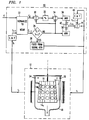
- FIG. 1 there is shown a block diagram of a differential process controller 10, in accordance with a preferred embodiment of the invention, for controlling a prior-art chemical vapor deposition reactor 12 which serves to epitaxially grow layers of atoms on a batch of semiconductor wafers 14.
- a prior-art chemical vapor deposition reactor 12 which serves to epitaxially grow layers of atoms on a batch of semiconductor wafers 14.
- the reactor 12 is merely exemplary of a wide variety of process equipment capable of being controlled by the controller 10 of FIG. 1.
- the chemical vapor deposition system 12 typically comprises a susceptor 16 situated in a glass bell jar-like enclosure 18.
- the susceptor 16 typically takes the form of a multi-sided, heated body that is rotatable about a vertical axis 20.
- the susceptor 16 is made from graphite or the like. Additional heating means (not shown), typically in the form of infrared lamps, surround the enclosure 18 to further heat the susceptor 16.
- each side of the susceptor 16 serves to hold three wafers 14a, 14b and 14c at the top, middle and the bottom, respectively.
- a greater or lesser number of wafers 14 could be accommodated.
- the wafers 14a, 14b and 14c on each susceptor side are exposed to reactant-containing gases admitted into the enclosure 18 through each of a pair of diametrically opposed nozzles 22 and 24 situated at the upper end of the enclosure.
- the nozzles 22 and 24 are each rotatable through both vertical and horizontal arcs that sweep out vertical and horizontal curved surfaces, respectively, that are each tangent to a successive one of the susceptor sides.
- layers of atoms typically silicon
- the parameters having the largest influence on the layer thickness variations are the flow of reactant-containing gases through each of the nozzles 22 and 24 as well as the vertical and horizontal nozzle angle orientation.
- the flow of reactant-containing gas through each of the nozzles 22 and 24 is determined by the degree to which each of a pair of control valves (not shown), associated with a separate one of the nozzles, is opened.
- the chemical vapor deposition reactor 12 is responsive to a control vector c r , generated at successive intervals ( r , r + 1, r + 2).
- the controller 10 operates to generate the control vector c r in accordance with two input vectors, t d , representing a desired set of process outputs, and the second vector t r , representing an actual set of process output values.
- the vector t d represents a set of desired layer thickness values
- the vector t r represents actual wafer thicknesses at a time r .
- the vectors t d and t r typically each contain five thickness measurements associated with each of the three wafers 14a, 14b and 14c, so that each vector contain fifteen values in all.
- the thickness is measured at the center of the wafer, and each of four other points north, east, west and south of the wafer center.
- the wafer thickness values can be obtained manually, using destructive sampling techniques, or could be obtained using automatic measurement techniques.
- the vector t d is typically generated by an external source (not shown) and is supplied to the controller for input to a processing element 22 that serves to normalize the vector to a mean value t ' d to facilitate processing thereof.
- the vector t r which is generated by the chemical vapor deposition reactor 12, is input to the controller 10 for receipt at a store and forward element 24.
- the store and forward element 24 acts to delay the receipt of the vector t r at the processing element 22 by a prescribed time so that the actual process output values received at the processing element effectively represent those process output values generated during the previous interval r -1. For this reason, the vector supplied by the store and forward element 24 to the processing element 22 is designated as t r-1 so that the normalized value thereof is designated as t ' r-1 .
- the purpose in having the processing element 22 normalize the vectors t d and t r-1 to a mean value is to transform the signals for representing the uniformity of layer thickness which is of concern in this process. (Note that the actual value of the mean layer thickness can be controlled by means of other process parameters.) Note that while desirable, normalization of the vectors t d and t r -1 is not critical. Therefore, the processing element 22 could be omitted from the controller 10.
- the vector t ' r -1 output by the processing element 22 is sampled and compared to the vector t ' d at a gate 26. Should the difference between two vectors fall within a preset tolerance limit, indicating that the actual wafer thicknesses closely correspond to the desired wafer thicknesses, then a signal generator 28 generates a control vector c r at a fixed level to maintain the chemical vapor deposition reactor 12 in a steady state, so that the reactor continues to produce wafers 14a, 14b and 14c having a substantially uniform thickness.
- the presence of the gate 26 and the signal generator 28 is not critical to the controller operation.
- the vector t ' r -1 is inverted and then summed with t ' d at a first summing amplifier 30 that computes the vector difference between them.
- a scaling amplifier 32 scales the output vector produced by the summing amplifier 30 by a constant k that is typically, although not necessarily, set equal to unity. It may be appropriate to set the value of ⁇ to 0.5 or less when a large difference between the actual process characteristics and the inverse model characteristics is expected.
- the output signal of the scalar 32 is input to a first non-invert input of a second summing amplifier 34 having a second non-invert input supplied with the vector t ' r -1 generated by the processing element 22.
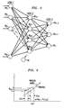
- the output signal of the summing amplifier 34 which varies with the vector t ' d , is input to a first artificial neural network 36 while the vector t ' r -1 generated by the processing element 22 is input to a second neural network 38.
- the artificial neural networks 36 and 38 are identical in structure and operation. (In fact, while the controller 10 has been described as comprising two artificial neural networks 34 and 36, a single one of the networks could be used to process the vectors t ' d and t r -1 on a successive basis.) Since the artificial neural networks are identical, only the artificial neural network 36 will be described in detail.
- the artificial neural network 36 is comprised of a plurality of nodes 401,402,403...40 n -2 ,40 n -1 and 40 n , where n is an integer dependent on the number of components of the vectors t d , t r -1 and c r .
- the network 36 also includes a bias signal generator 40 which supplies each the nodes 4016 - 40 n with a constant level signal, typically -1.
- the nodes 401 -40 n in the artificial neural network 36 are arranged in three separate layers, depicted in FIG. 2 as layers 1, 2 and 3, respectively. There are fifteen nodes (401-4015) in layer 1, which is designated as the input layer because each of the nodes in this layer is supplied with a separate one of the fifteen components of the input signal supplied by the summing amplifier 34 to the artificial neural network 36. In practice, the number of nodes in layer 1 may be greater or smaller than the fifteen nodes shown in FIG. 2 if there is a larger or smaller number of components in the input signal supplied to the artificial neural network 36.
- Layer 3 has three nodes 40 n -2 , 40 n -1 and 40 n and is designated as the output layer because each of the nodes 40 n -2 , 40 n -1 and 40 n in this layer generates a signal which serves as a separate one of the components of the vector c r produced by the controller 10.
- There are four nodes 4016-4019 in layer 2 which is designated as the "hidden” layer because the nodes therein neither receive an external input nor do they supply an external output signal. Instead, each of the nodes 4016-4019 in layer 2 is supplied with the output signal of each of the nodes 401-4015 in layer 1.
- each of the nodes 4016-4019 supplies its output signal to a separate one of the nodes 40 n -2 ,40 n -1 and 40 n .
- the nodes 401-4015 in layer 1 act simply to distribute each of the received input signals to a separate one of the nodes 4016-4019 in the second layer.
- the nodes 4016-4019 and 40 n -2 , 40 n -1 and 40 n serve to appropriately scale the signal supplied thereto, then sum the signals before transforming the sum according to a non-linear relationship, for instance a tan-hyperbolic function (tanh).
- tanh tan-hyperbolic function
- the network 36 is trained in accordance with a training data set obtained from experiments and/or operational data, so that the network serves as a model of the chemical vapor deposition reactor 12.
- the connection weight between the nodes 401-40 n is adjusted, based on the training data presented to the artificial neural network 36, so that the network generates the control vector c r to drive the chemical vapor deposition reactor 12 to yield the input signals supplied to the network.
- the error signal i.e., the difference between the actual process output and the estimated neural network output
- Such training techniques are well known in the art.
- the network 36 could be configured of three separate subnetworks (not shown) each having the same first and second layers but a single-node output layer generating a separate component of c r .
- the advantage of this approach is that each subnetwork can be more easily trained using a smaller training set.
- the disadvantage is that the overall network 36 is made larger.
- mapping procedure it is desirable to have a data set (training and test) with a one-to-one or many-to-one mapping where a given input always maps to a given output. This is true in training artificial neural networks as well.
- the invention is robust to the differences between the predictor and the process if the first and second order statistics do not change sign. This is due to the fact that the predictor output difference is used instead of the output values for predicting the control parameters for the next iteration.
- the output signal produced by the artificial neural network 36 is supplied to a non-invert input of a summing amplifier 42 that also has an invert input supplied with the output signal of the artificial neural network 38.
- the summing amplifier 42 generates an output signal in accordance with the difference between the output signals of the artificial neural networks 36 and 38. Since each of the artificial neural networks 36 and 38 generates a control signal in accordance with a separate one of the input vectors t ' d and t ' r -1 , respectively, the output of the summing amplifier 42 thus represents the difference between the two control signals. For this reason, the output signal of the summing amplifier 42 is given the designation ⁇ c r .
- the output signal produced by the summing amplifier 42 is input to a first non-invert input of a summing amplifier 44 whose output serves as the control signal c r .
- the summing amplifier 44 has a second non-invert which is supplied with the output of the summing amplifier, as delayed by a store and forward device 46, identical to the store and forward device 24.
- the store and forward device effectively serves to supply the second non-invert input of the summing amplifier 44 with the signal c r generated by the summing amplifier at a previous interval ( r -1).
- the signal supplied to the second input of the summing amplifier 44 is designated as c r -1 .
- the summing amplifier 44 produces the signal c r at its output in accordance with the sum of ⁇ c r and c r -1 .
- the controller 10 operates to produce a control signal c r in accordance with the sum of c r -1 , representing the control signal generated during the previous interval r -1, and ⁇ c r , representing the difference between the artificial neural network 36 and 38 output signals.
- each of the artificial neural networks 36 and 38 produces a control signal in accordance with a separate one of the input vectors t d and t r -1 , the latter representing actual process output values produced during the interval r -1.
- the controller 10 operates to control the chemical vapor deposition reactor 12 in accordance with both the actual and desired process output values, which, in the case of the chemical vapor deposition reactor 12, are the actual and desired thicknesses for the wafers 14a, 14b and 14c of FIG. 1, the actual thickness values representing process feedback.
- FIG. 3 shows a pair of plots graphically depicting the relationship between a scalar representation of the control vector c r input to the chemical vapor deposition reactor 12 and a scalar representation of the process output values (e.g., wafer 14a, 14b and 14c layer thicknesses).
- the solid plot represents the normally unknown actual relationship between c r and wafer thickness of the process itself whereas the dashed plot represents the ideal relationship between c r and wafer thickness, as modelled by each of the artificial neural networks 36 and 38.
- controller 10 for controlling a process using both desired and actual process values with at least one, and preferably a pair of artificial neural network 36 and 38.
- controller 10 has been described as being configured of individual hardware elements 22-46, the functions of these elements could easily be practiced collectively using a single, general purpose digital computer. Rather than configure the controller 10 of a pair of artificial neural networks 36 and 38 either in hardware or software, a single neural network could be employed to process the output signal of the summing amplifier 34 and the gate 26 in succession.
Abstract
Description
- This invention relates to a method and apparatus which employs at least one artificial neural network for iteratively controlling a process in accordance with both a set of optimal process output values and a set of actual process output values generated during a previous iteration.
- The manufacture of high quality product on a repeated basis requires accurate control of the manufacturing process. The fabrication of semiconductor wafers by the well-known planar process is no exception to this rule. Among the steps carried out to fabricate a semiconductor wafer by the planar process is that of epitaxial layer growth whereby a semiconductor wafer is subjected to chemical vapor deposition to grow up layers of atoms on the surface of the wafer. With silicon semiconductor devices, such chemical vapor deposition is typically carried out by heating the wafers in a reactor while hydrogen and silicon tetrachloride are reacted, or alternatively, silane is decomposed, to deposit silicon atoms on the wafer surface.
- To obtain high quality semiconductor devices, the thickness of each layer of atoms grown on the wafer by chemical vapor deposition should be uniform across the wafer surface. The conventional approach to controlling layer thickness is to fabricate a small batch of wafers and then measure the layer thickness uniformity. To compensate for any such non-uniformity, adjustments are then made to the process. Once such adjustments are made, another batch of wafers is fabricated and thereafter, the layer thickness again measured. Depending on the degree of layer thickness uniformity that is wanted, these steps may be carried out many times.
- In an effort to obtain more precise control of manufacturing processes, including the above-described chemical vapor deposition process, artificial neural networks have been employed. Such artificial neural networks are comprised of a plurality of simple computing elements, a number of which function as simple, non-linear summing nodes, connected together with varying strengths, to mimic the operation of the human brain. A typical artificial neural network is comprised of a plurality of such nodes arranged in two or more layers, with the nodes in the first layer typically each serving to receive a separate one of the input signals and distribute the signal to a separate one of the nodes in the second layer. The nodes in the second layer each function as a non-linear summing node to transform the input signals supplied thereto from the nodes in the previous layer for receipt as an output of the network if only two layers are present, or if a third layer of nodes is present, for receipt at the input of the nodes in such a layer. The nodes in each subsequent layer transform the signal received thereto, with the nodes in the last layer yielding a separate one of the network output signals.
- Each node in the artificial neural network (except those nodes in the first layer) serves to: (1) multiply each incoming input signal by a separate scaling factor (referred to as a connection weight), (2) sum the resulting weighted signals, and (3) transform the sum according to a non-linear relationship, such as a sigmoid or tanhyperbolic function. The artificial neural network is "trained," that is to say, the connection weights of the nodes in the second and subsequent layers are adjusted in accordance with past data so that the network serves as an inverse model of the process being controlled. In other words, the artificial neural network functions to transform a set of actual output values of a process to yield a process-driving signal to control the process to produce output values more closely approximating a desired set of values.
- The disadvantage of most present-day control schemes that employ artificial neural networks is that there is little, if any, feedback of the actual process output signals back into the neural network. As a result, process control is less precise, a distinct disadvantage. Further, most present day control schemes using artificial neural networks are not responsive to the differences between actual process values and a predictor of the process.
- In practice, there is generally a difference between the process characteristics and the predictor or estimator. These differences may be due to predictor error, process drift, the failure to account for the effect of an unknown or excluded parameter, or some other reason.
- Thus there is a need for an artificial neural network control system that is robust to the differences between the predictor and the process under the conditions where the first and second order statistics do not change.
- Briefly, in accordance with a preferred embodiment of the invention, there is provided a differential process controller, as recited in
claim 1, and a differential process control method as recited in claim 6. -
- FIGURE 1 is a block diagram of a differential process controller, in accordance with the invention, for controlling a chemical vapor deposition system;
- FIGURE 2 is a simplified block diagram of one of a pair of neural networks within the controller of FIG. 1; and
- FIGURE 3 is a graphical scalar representation of the relationship between the process input values and output values for the controller of FIG. 1
- In FIG. 1 there is shown a block diagram of a
differential process controller 10, in accordance with a preferred embodiment of the invention, for controlling a prior-art chemicalvapor deposition reactor 12 which serves to epitaxially grow layers of atoms on a batch of semiconductor wafers 14. As will be appreciated from a detailed discussion of the invention provided hereinafter, thereactor 12 is merely exemplary of a wide variety of process equipment capable of being controlled by thecontroller 10 of FIG. 1. - To understand the manner in which the
controller 10 operates to control the chemicalvapor deposition reactor 12, a brief overview of the chemical vapor deposition system will prove useful. In the illustrated embodiment, the chemicalvapor deposition system 12 typically comprises asusceptor 16 situated in a glass bell jar-like enclosure 18. Thesusceptor 16 typically takes the form of a multi-sided, heated body that is rotatable about a vertical axis 20. In practice, thesusceptor 16 is made from graphite or the like. Additional heating means (not shown), typically in the form of infrared lamps, surround theenclosure 18 to further heat thesusceptor 16. - On each of the sides of the
susceptor 16 are pockets, each holding a separate one of a set of wafers 14. In the illustrated embodiment, each side of thesusceptor 16 serves to hold threewafers susceptor 16, a greater or lesser number of wafers 14 could be accommodated. - As the
susceptor 16 rotates about its axis, thewafers enclosure 18 through each of a pair of diametrically opposednozzles 22 and 24 situated at the upper end of the enclosure. Thenozzles 22 and 24 are each rotatable through both vertical and horizontal arcs that sweep out vertical and horizontal curved surfaces, respectively, that are each tangent to a successive one of the susceptor sides. As the reactant-containing gases contact each of thewafers - To fabricate high quality wafers 14, uniformity of deposition is usually critical, not only across each wafer, but across the
wafers susceptor 16. Accordingly, it is desirable to control the chemicalvapor deposition reactor 12 to minimize such variation. In practice, the parameters having the largest influence on the layer thickness variations are the flow of reactant-containing gases through each of thenozzles 22 and 24 as well as the vertical and horizontal nozzle angle orientation. The flow of reactant-containing gas through each of thenozzles 22 and 24 is determined by the degree to which each of a pair of control valves (not shown), associated with a separate one of the nozzles, is opened. To control these parameters, and thereby minimize layer thickness variation, the chemicalvapor deposition reactor 12 is responsive to a control vector c r , generated at successive intervals (r,r + 1,r + 2...). The control vector c r includes the following three components c¹, c², and c³:
c² = angle of each ofnozzles 22 and 24 from horizontal plane
c³ = angle of each ofnozzles 22 and 24 from vertical plane - In general, the
controller 10 operates to generate the control vector c r in accordance with two input vectors, t d , representing a desired set of process outputs, and the second vector t r , representing an actual set of process output values. In the illustrated embodiment, the vector t d represents a set of desired layer thickness values whereas the vector t r represents actual wafer thicknesses at a time r. - The vectors t d and t r typically each contain five thickness measurements associated with each of the three
wafers wafers - The vector t d is typically generated by an external source (not shown) and is supplied to the controller for input to a
processing element 22 that serves to normalize the vector to a mean value t' d to facilitate processing thereof. Unlike the vector t d that is immediately normalized, the vector t r , which is generated by the chemicalvapor deposition reactor 12, is input to thecontroller 10 for receipt at a store and forward element 24. The store and forward element 24 acts to delay the receipt of the vector t r at theprocessing element 22 by a prescribed time so that the actual process output values received at the processing element effectively represent those process output values generated during the previous interval r-1. For this reason, the vector supplied by the store and forward element 24 to theprocessing element 22 is designated as t r-1 so that the normalized value thereof is designated as t' r-1 . - The purpose in having the
processing element 22 normalize the vectors t d and t r-1 to a mean value is to transform the signals for representing the uniformity of layer thickness which is of concern in this process. (Note that the actual value of the mean layer thickness can be controlled by means of other process parameters.) Note that while desirable, normalization of the vectors t d and t r-1 is not critical. Therefore, theprocessing element 22 could be omitted from thecontroller 10. - In practice, the vector t' r-1 output by the
processing element 22 is sampled and compared to the vector t' d at agate 26. Should the difference between two vectors fall within a preset tolerance limit, indicating that the actual wafer thicknesses closely correspond to the desired wafer thicknesses, then asignal generator 28 generates a control vector c r at a fixed level to maintain the chemicalvapor deposition reactor 12 in a steady state, so that the reactor continues to producewafers controller 10, the presence of thegate 26 and thesignal generator 28 is not critical to the controller operation. As will be appreciated from a description of the remaining portion of thecontroller 10 provided below, when t' d corresponds to t' r-1, even in the absence of thegate 26 andsignal generator 28, the controller will maintain the chemicalvapor deposition system 12 in a steady state. Thus, thegate 26 andsignal generator 28, while useful, could be deleted from the controller without any adverse effect on its operation. However, it helps to detect any undesired variation due to other parameter changes and to bring the process back in control. - In the absence of a close correspondence between t' d and t' r-1, the vector t' r-1 is inverted and then summed with t' d at a first summing
amplifier 30 that computes the vector difference between them. A scalingamplifier 32 scales the output vector produced by the summingamplifier 30 by a constant k that is typically, although not necessarily, set equal to unity. It may be appropriate to set the value of κ to 0.5 or less when a large difference between the actual process characteristics and the inverse model characteristics is expected. The output signal of the scalar 32 is input to a first non-invert input of a second summingamplifier 34 having a second non-invert input supplied with the vector t' r-1 generated by theprocessing element 22. The summingamplifier 34 adds the two input signals supplied to its two inputs and yields an output signal varying with t' d . (In fact when k = 1, the output signal of the summingamplifier 34 corresponds exactly to the signal t' d .) - The output signal of the summing
amplifier 34, which varies with the vector t' d , is input to a first artificialneural network 36 while the vector t' r-1 generated by theprocessing element 22 is input to a secondneural network 38. - The artificial
neural networks controller 10 has been described as comprising two artificialneural networks neural network 36 will be described in detail. - Referring to FIG. 2, the artificial
neural network 36 is comprised of a plurality ofnodes network 36 also includes abias signal generator 40 which supplies each the nodes 40₁₆ - 40 n with a constant level signal, typically -1. - The nodes 40₁ -40 n in the artificial
neural network 36 are arranged in three separate layers, depicted in FIG. 2 aslayers layer 1, which is designated as the input layer because each of the nodes in this layer is supplied with a separate one of the fifteen components of the input signal supplied by the summingamplifier 34 to the artificialneural network 36. In practice, the number of nodes inlayer 1 may be greater or smaller than the fifteen nodes shown in FIG. 2 if there is a larger or smaller number of components in the input signal supplied to the artificialneural network 36. -
Layer 3 has threenodes nodes controller 10. There are four nodes 40₁₆-40₁₉ inlayer 2 which is designated as the "hidden" layer because the nodes therein neither receive an external input nor do they supply an external output signal. Instead, each of the nodes 40₁₆-40₁₉ inlayer 2 is supplied with the output signal of each of the nodes 40₁-40₁₅ inlayer 1. By the same token, instead of generating an external output signal, each of the nodes 40₁₆-40₁₉ supplies its output signal to a separate one of thenodes - The nodes 40₁-40₁₅ in
layer 1 act simply to distribute each of the received input signals to a separate one of the nodes 40₁₆-40₁₉ in the second layer. The nodes 40₁₆-40₁₉ and 40 n-2, 40 n-1 and 40 n serve to appropriately scale the signal supplied thereto, then sum the signals before transforming the sum according to a non-linear relationship, for instance a tan-hyperbolic function (tanh). - The
network 36 is trained in accordance with a training data set obtained from experiments and/or operational data, so that the network serves as a model of the chemicalvapor deposition reactor 12. In other words, the connection weight between the nodes 40₁-40 n is adjusted, based on the training data presented to the artificialneural network 36, so that the network generates the control vector c r to drive the chemicalvapor deposition reactor 12 to yield the input signals supplied to the network. In this training method, the error signal (i.e., the difference between the actual process output and the estimated neural network output) is back-propagated through the neural network for modifying the connection weights. Such training techniques are well known in the art. - As an alternative implementation, the
network 36 could be configured of three separate subnetworks (not shown) each having the same first and second layers but a single-node output layer generating a separate component of c r . The advantage of this approach is that each subnetwork can be more easily trained using a smaller training set. The disadvantage is that theoverall network 36 is made larger. - As in any mapping procedure, it is desirable to have a data set (training and test) with a one-to-one or many-to-one mapping where a given input always maps to a given output. This is true in training artificial neural networks as well. The invention is robust to the differences between the predictor and the process if the first and second order statistics do not change sign. This is due to the fact that the predictor output difference is used instead of the output values for predicting the control parameters for the next iteration.
- Referring to FIG. 1, the output signal produced by the artificial
neural network 36 is supplied to a non-invert input of a summingamplifier 42 that also has an invert input supplied with the output signal of the artificialneural network 38. The summingamplifier 42 generates an output signal in accordance with the difference between the output signals of the artificialneural networks neural networks amplifier 42 thus represents the difference between the two control signals. For this reason, the output signal of the summingamplifier 42 is given the designation Δc r . - The output signal produced by the summing
amplifier 42, representing the difference between the control signals produced by the artificialneural networks forward device 46, identical to the store and forward device 24. The store and forward device effectively serves to supply the second non-invert input of the summing amplifier 44 with the signal c r generated by the summing amplifier at a previous interval (r-1). Thus the signal supplied to the second input of the summing amplifier 44 is designated as c r-1. In this way, the summing amplifier 44 produces the signal c r at its output in accordance with the sum of Δc r and c r-1. - In operation, the
controller 10 operates to produce a control signal c r in accordance with the sum of c r-1, representing the control signal generated during the previous interval r-1, and Δc r , representing the difference between the artificialneural network neural networks controller 10 operates to control the chemicalvapor deposition reactor 12 in accordance with both the actual and desired process output values, which, in the case of the chemicalvapor deposition reactor 12, are the actual and desired thicknesses for thewafers - To better understand the manner in which the
controller 10 operates, reference should be had to FIG. 3 which shows a pair of plots graphically depicting the relationship between a scalar representation of the control vector c r input to the chemicalvapor deposition reactor 12 and a scalar representation of the process output values (e.g.,wafer neural networks vapor deposition reactor 12 is c r-1, the actual wafer thicknesses vector corresponds to t r-1, not t d , the desired thickness. Using the model of the process, (as represented by the dashed line ), it thus becomes necessary to increase the value of the control vector by Δc r in order to achieve wafer thicknesses closer to the desired wafer thickness values t d . - The foregoing describes a
controller 10 for controlling a process using both desired and actual process values with at least one, and preferably a pair of artificialneural network - It is to be understood that the above-described embodiments are merely illustrative of the principles of the invention. Various modifications and changes may be made thereto by those skilled in the art.
- For example, while the
controller 10 has been described as being configured of individual hardware elements 22-46, the functions of these elements could easily be practiced collectively using a single, general purpose digital computer. Rather than configure thecontroller 10 of a pair of artificialneural networks amplifier 34 and thegate 26 in succession.
Claims (8)
- A differential process controller for controlling a process at a time r in accordance with both an optimal process output value vector (t d ), whose components represent desired process values, and an actual process value vector (t r-1), whose components represent actual process values measured during an immediately previous interval (r-1), CHARACTERIZED BY:
first processing means (22,30,32,34) responsive to the optimal process output value vector t d for generating a first vector varying in accordance therewith;
a first artificial neural network (36) for processing the first vector in accordance with past actual process values to yield a first intermediate control vector for controlling the process;
second processing means (26) responsive to the actual process value vector t r-1 for generating a second vector varying in accordance therewith;
a second artificial neural network (38) for processing the second vector in accordance with past actual process values to yield a second intermediate control vector for controlling the process;
a first summing amplifier (42) for producing an output signal varying in accordance with the difference between the first and second intermediate control vectors;
a second summing amplifier (44) having a first input supplied with the output of the first summing amplifier, and a second input, for generating a control vector for controlling the process in accordance with the sum of the signals at the first and second summing amplifier inputs; and
a store and forward means (46) supplied with the control signal from the second summing amplifier for storing said control signal and thereafter supplying said signal to said second input of said second summing amplifier at a later interval. - The apparatus according to claim 1 wherein each of the first and second artificial neural networks comprises:
a first layer of nodes (40₁-40₁₅), each receiving a separate one of the components of the input vector supplied to the network for distributing the vector component supplied thereto;
a second layer of nodes (40₁₆-40₁₉), each supplied with the signal distributed by each of the nodes in the first layer for transforming the signals supplied thereto; and
a third layer of nodes (40 n-2-40 n ), each supplied with the scaled signal produced by each of the nodes in the second layer for transforming the signals supplied thereto to yield a separate component of the intermediate control vector output by the network. - The apparatus according to claim 1 wherein said first processing means comprises:
a processing element (22) for normalizing each of the optimal process output vectors t d and the actual process value vectors t r-1 to a mean value;
a third summing amplifier (30) supplied with the normalized-to-mean values of the vectors t d and t r-1 and generating an output vector varying in accordance with the difference therebetween;
scaling means (32) for scaling the output vector produced by the third summing amplifier by a constant value;
a fourth summing amplifier (34) for summing the output of the scaling means and with the normalized value of the vector t r-1. - The apparatus according to claim 1 wherein the second processing means includes a processing element (22) for normalizing the actual process value vector to a mean value.
- The apparatus according to claim 3 further including:
means (22) for comparing the normalized value of the vector t r-1 to a vector representing the normalized value of the vector t d ; and
a signal generator (28) for generating a fixed-value control vector for controlling the process when the difference between the normalized values of the vectors t d and t r-1 is within a prescribed tolerance value. - A method for controlling a process at a time r in accordance with both an optimal process output value vector (t d ), whose components represent desired process values, and an actual process value vector (t r-1), whose components represent actual process values measured during a previous interval (r-1),
CHARACTERIZED BY the steps of:
processing the optimal output value vector t d to yield a first vector varying in accordance therewith;
applying the first vector to an artificial neural network (36) which sums and transforms the components of the first vector in accordance with past actual process output values to yield a first intermediate control vector;
applying the second vector to an artificial neural network (38) which sums and transforms the components of the second vector in accordance with past actual process output values to yield a second intermediate control vector;
generating a differential control vector varying in accordance with the difference between the first and second intermediate control vectors;
successively generating a control vector in accordance with the sum of the differential control vector and the control vector generated during the immediately previous interval. - The method according to claim 5 wherein the optimal process value vector is processed by the steps of:
normalizing the optimal process vector t d to a mean value;
normalizing the actual process output value vector t r-1 to a mean value;
generating a difference vector in accordance with the normalized-to-mean values of the vectors t d and t r-1;
scaling the difference vector by a constant; and
summing the scaled difference vector with the normalized-to-mean value of the vector t r-1; - The method according to claim 5 wherein the actual process output value vector is processed by normalizing the vector to a mean value.
Applications Claiming Priority (2)
| Application Number | Priority Date | Filing Date | Title |
|---|---|---|---|
| US08/011,568 US5388186A (en) | 1993-02-01 | 1993-02-01 | Differential process controller using artificial neural networks |
| US11568 | 1996-02-13 |
Publications (2)
| Publication Number | Publication Date |
|---|---|
| EP0609999A1 true EP0609999A1 (en) | 1994-08-10 |
| EP0609999B1 EP0609999B1 (en) | 1996-07-24 |
Family
ID=21750969
Family Applications (1)
| Application Number | Title | Priority Date | Filing Date |
|---|---|---|---|
| EP94300417A Expired - Lifetime EP0609999B1 (en) | 1993-02-01 | 1994-01-19 | Differential process controller using artificial neural networks |
Country Status (4)
| Country | Link |
|---|---|
| US (1) | US5388186A (en) |
| EP (1) | EP0609999B1 (en) |
| JP (1) | JPH07182010A (en) |
| DE (1) | DE69400317T2 (en) |
Cited By (5)
| Publication number | Priority date | Publication date | Assignee | Title |
|---|---|---|---|---|
| DE19624301A1 (en) * | 1996-06-18 | 1998-01-08 | Siemens Ag | Learning method for neural network |
| DE19727795C1 (en) * | 1997-06-30 | 1998-12-17 | Siemens Ag | Process modelling method for neural network |
| EP1253497A1 (en) * | 2001-04-27 | 2002-10-30 | Infineon Technologies SC300 GmbH & Co. KG | Method for adjusting processing parameters of plate-like objects in a processing tool |
| EP1396770A1 (en) * | 2002-08-16 | 2004-03-10 | Powitec Intelligent Technologies GmbH | Method of regulating a thermodynamic process |
| EP3474090A1 (en) | 2017-10-20 | 2019-04-24 | aixprocess GmbH | Method for regulating a process within a system, in particular the combustion process of a boiler or furnace |
Families Citing this family (46)
| Publication number | Priority date | Publication date | Assignee | Title |
|---|---|---|---|---|
| JPH07141005A (en) * | 1993-06-21 | 1995-06-02 | Hitachi Ltd | Manufacture of semiconductor integrated circuit device and the device for the same |
| US5586221A (en) * | 1994-07-01 | 1996-12-17 | Syracuse University | Predictive control of rolling mills using neural network gauge estimation |
| US5943660A (en) * | 1995-06-28 | 1999-08-24 | Board Of Regents The University Of Texas System | Method for feedback linearization of neural networks and neural network incorporating same |
| US6850874B1 (en) | 1998-04-17 | 2005-02-01 | United Technologies Corporation | Method and apparatus for predicting a characteristic of a product attribute formed by a machining process using a model of the process |
| US9906838B2 (en) | 2010-07-12 | 2018-02-27 | Time Warner Cable Enterprises Llc | Apparatus and methods for content delivery and message exchange across multiple content delivery networks |
| US9015093B1 (en) | 2010-10-26 | 2015-04-21 | Michael Lamport Commons | Intelligent control with hierarchical stacked neural networks |
| US8775341B1 (en) | 2010-10-26 | 2014-07-08 | Michael Lamport Commons | Intelligent control with hierarchical stacked neural networks |
| US20120150334A1 (en) * | 2010-12-10 | 2012-06-14 | L'air Liquide Societe Anonyme Pour L'etude Et L'exploitation Des Procedes Georges Claude | Integrated Fault Detection And Analysis Tool |
| US8990133B1 (en) | 2012-12-20 | 2015-03-24 | Brain Corporation | Apparatus and methods for state-dependent learning in spiking neuron networks |
| US9566710B2 (en) | 2011-06-02 | 2017-02-14 | Brain Corporation | Apparatus and methods for operating robotic devices using selective state space training |
| US20130151449A1 (en) * | 2011-12-07 | 2013-06-13 | Filip Ponulak | Apparatus and methods for implementing learning for analog and spiking signals in artificial neural networks |
| US9104186B2 (en) | 2012-06-04 | 2015-08-11 | Brain Corporation | Stochastic apparatus and methods for implementing generalized learning rules |
| US9156165B2 (en) | 2011-09-21 | 2015-10-13 | Brain Corporation | Adaptive critic apparatus and methods |
| US9213937B2 (en) | 2011-09-21 | 2015-12-15 | Brain Corporation | Apparatus and methods for gating analog and spiking signals in artificial neural networks |
| US9015092B2 (en) | 2012-06-04 | 2015-04-21 | Brain Corporation | Dynamically reconfigurable stochastic learning apparatus and methods |
| US9146546B2 (en) | 2012-06-04 | 2015-09-29 | Brain Corporation | Systems and apparatus for implementing task-specific learning using spiking neurons |
| US8943008B2 (en) | 2011-09-21 | 2015-01-27 | Brain Corporation | Apparatus and methods for reinforcement learning in artificial neural networks |
| US9256215B2 (en) | 2012-07-27 | 2016-02-09 | Brain Corporation | Apparatus and methods for generalized state-dependent learning in spiking neuron networks |
| US9189730B1 (en) | 2012-09-20 | 2015-11-17 | Brain Corporation | Modulated stochasticity spiking neuron network controller apparatus and methods |
| US9367798B2 (en) | 2012-09-20 | 2016-06-14 | Brain Corporation | Spiking neuron network adaptive control apparatus and methods |
| US9082079B1 (en) | 2012-10-22 | 2015-07-14 | Brain Corporation | Proportional-integral-derivative controller effecting expansion kernels comprising a plurality of spiking neurons associated with a plurality of receptive fields |
| US9195934B1 (en) | 2013-01-31 | 2015-11-24 | Brain Corporation | Spiking neuron classifier apparatus and methods using conditionally independent subsets |
| US9764468B2 (en) | 2013-03-15 | 2017-09-19 | Brain Corporation | Adaptive predictor apparatus and methods |
| US9008840B1 (en) | 2013-04-19 | 2015-04-14 | Brain Corporation | Apparatus and methods for reinforcement-guided supervised learning |
| US9242372B2 (en) | 2013-05-31 | 2016-01-26 | Brain Corporation | Adaptive robotic interface apparatus and methods |
| US9384443B2 (en) | 2013-06-14 | 2016-07-05 | Brain Corporation | Robotic training apparatus and methods |
| US9792546B2 (en) | 2013-06-14 | 2017-10-17 | Brain Corporation | Hierarchical robotic controller apparatus and methods |
| US9314924B1 (en) * | 2013-06-14 | 2016-04-19 | Brain Corporation | Predictive robotic controller apparatus and methods |
| US9436909B2 (en) | 2013-06-19 | 2016-09-06 | Brain Corporation | Increased dynamic range artificial neuron network apparatus and methods |
| US9296101B2 (en) | 2013-09-27 | 2016-03-29 | Brain Corporation | Robotic control arbitration apparatus and methods |
| US9579789B2 (en) | 2013-09-27 | 2017-02-28 | Brain Corporation | Apparatus and methods for training of robotic control arbitration |
| US9489623B1 (en) | 2013-10-15 | 2016-11-08 | Brain Corporation | Apparatus and methods for backward propagation of errors in a spiking neuron network |
| US9597797B2 (en) | 2013-11-01 | 2017-03-21 | Brain Corporation | Apparatus and methods for haptic training of robots |
| US9463571B2 (en) | 2013-11-01 | 2016-10-11 | Brian Corporation | Apparatus and methods for online training of robots |
| US9248569B2 (en) | 2013-11-22 | 2016-02-02 | Brain Corporation | Discrepancy detection apparatus and methods for machine learning |
| US9358685B2 (en) | 2014-02-03 | 2016-06-07 | Brain Corporation | Apparatus and methods for control of robot actions based on corrective user inputs |
| US9630317B2 (en) | 2014-04-03 | 2017-04-25 | Brain Corporation | Learning apparatus and methods for control of robotic devices via spoofing |
| US9613308B2 (en) | 2014-04-03 | 2017-04-04 | Brain Corporation | Spoofing remote control apparatus and methods |
| US9346167B2 (en) | 2014-04-29 | 2016-05-24 | Brain Corporation | Trainable convolutional network apparatus and methods for operating a robotic vehicle |
| US9849588B2 (en) | 2014-09-17 | 2017-12-26 | Brain Corporation | Apparatus and methods for remotely controlling robotic devices |
| US9821470B2 (en) | 2014-09-17 | 2017-11-21 | Brain Corporation | Apparatus and methods for context determination using real time sensor data |
| US9860077B2 (en) | 2014-09-17 | 2018-01-02 | Brain Corporation | Home animation apparatus and methods |
| US9579790B2 (en) | 2014-09-17 | 2017-02-28 | Brain Corporation | Apparatus and methods for removal of learned behaviors in robots |
| US9630318B2 (en) | 2014-10-02 | 2017-04-25 | Brain Corporation | Feature detection apparatus and methods for training of robotic navigation |
| US9717387B1 (en) | 2015-02-26 | 2017-08-01 | Brain Corporation | Apparatus and methods for programming and training of robotic household appliances |
| US10295972B2 (en) | 2016-04-29 | 2019-05-21 | Brain Corporation | Systems and methods to operate controllable devices with gestures and/or noises |
Family Cites Families (2)
| Publication number | Priority date | Publication date | Assignee | Title |
|---|---|---|---|---|
| US5159660A (en) * | 1990-08-09 | 1992-10-27 | Western Thunder | Universal process control using artificial neural networks |
| US5285377A (en) * | 1990-10-30 | 1994-02-08 | Fujitsu Limited | Control apparatus structuring system |
-
1993
- 1993-02-01 US US08/011,568 patent/US5388186A/en not_active Expired - Lifetime
-
1994
- 1994-01-19 DE DE69400317T patent/DE69400317T2/en not_active Expired - Fee Related
- 1994-01-19 EP EP94300417A patent/EP0609999B1/en not_active Expired - Lifetime
- 1994-01-31 JP JP6025905A patent/JPH07182010A/en active Pending
Non-Patent Citations (2)
| Title |
|---|
| M.PALANISWAMI, V. PANG AND G. FENG: "SOME ISSUES WITH THE INTELLIGENT CONTROL OF INDUSTRIAL PROCESSES", TENCON '89, November 1989 (1989-11-01), BOMBAY INDIA, pages 1021 - 1024 * |
| T. YAMADA AND T.YABUTA: "NON-LINEAR NEURAL NETWORK CONTROLLER FOR DYNAMIC SYSTEM", IECON '90, vol. II, November 1990 (1990-11-01), PACIFIC GROVE US, pages 1244 - 1249 * |
Cited By (8)
| Publication number | Priority date | Publication date | Assignee | Title |
|---|---|---|---|---|
| DE19624301A1 (en) * | 1996-06-18 | 1998-01-08 | Siemens Ag | Learning method for neural network |
| DE19624301B4 (en) * | 1996-06-18 | 2006-08-17 | Siemens Ag | Learning method for a neural network |
| DE19727795C1 (en) * | 1997-06-30 | 1998-12-17 | Siemens Ag | Process modelling method for neural network |
| EP1253497A1 (en) * | 2001-04-27 | 2002-10-30 | Infineon Technologies SC300 GmbH & Co. KG | Method for adjusting processing parameters of plate-like objects in a processing tool |
| WO2002088858A1 (en) * | 2001-04-27 | 2002-11-07 | Infineon Technologies Sc300 Gmbh & Co. Kg | Method for adjusting processing parameters of at least one plate-like object in a processing tool |
| US6892108B2 (en) | 2001-04-27 | 2005-05-10 | Infineon Technologies Sc300 Gmbh & Co. Kg | Method for adjusting processing parameters of at least one plate-shaped object in a processing tool |
| EP1396770A1 (en) * | 2002-08-16 | 2004-03-10 | Powitec Intelligent Technologies GmbH | Method of regulating a thermodynamic process |
| EP3474090A1 (en) | 2017-10-20 | 2019-04-24 | aixprocess GmbH | Method for regulating a process within a system, in particular the combustion process of a boiler or furnace |
Also Published As
| Publication number | Publication date |
|---|---|
| EP0609999B1 (en) | 1996-07-24 |
| DE69400317D1 (en) | 1996-08-29 |
| JPH07182010A (en) | 1995-07-21 |
| DE69400317T2 (en) | 1996-12-05 |
| US5388186A (en) | 1995-02-07 |
Similar Documents
| Publication | Publication Date | Title |
|---|---|---|
| EP0609999B1 (en) | Differential process controller using artificial neural networks | |
| US5649063A (en) | Feedback process control using a neural network parameter estimator | |
| Ingolfsson et al. | Stability and sensitivity of an EWMA controller | |
| US5467883A (en) | Active neural network control of wafer attributes in a plasma etch process | |
| US6162488A (en) | Method for closed loop control of chemical vapor deposition process | |
| US6289508B1 (en) | Method and apparatus for dynamic optimization | |
| Adivikolanu et al. | Extensions and performance/robustness tradeoffs of the EWMA run-to-run controller by using the internal model control structure | |
| EP0879547A2 (en) | Model-based predictive control of thermal processing | |
| CN106521459B (en) | A kind of optimization method of MOCVD device growth uniformity technological parameter | |
| US6726767B1 (en) | Layer processing | |
| EP0119765B1 (en) | Sampled-data 1-pd control apparatus | |
| US20040173599A1 (en) | Multi-parameter process and control method | |
| US5244500A (en) | Process control system of semiconductor vapor phase growth apparatus | |
| Yusupbekov et al. | Stable algorithms for adaptive control and adaptation of uncertain dynamic objects based on reference models | |
| EP0602855A1 (en) | Active neural network control of wafer attributes in a plasma etch process | |
| Saraswat et al. | Rapid thermal multiprocessing for a programmable factory for adaptable manufacturing of ICs | |
| Camacho et al. | Implementation of self‐tuning generalized predictive controllers for the process industry | |
| Sherwin et al. | The optimization of InxGa1− xAs and InP growth conditions by CBE | |
| El-Awady et al. | Improvements in C/sub pk/using real-time feedback control | |
| Ingolfsson | Run by run process control | |
| Boyd et al. | Run by run (generalized SPC) control of semiconductor processes on the production floor | |
| EP1123562B1 (en) | Layer processing | |
| Winn | Optimal estimation of unmodeled accelerations on the ONERA navigational satellite | |
| Phillips | A very simple application of Kalman filtering to meteorological data assimilation | |
| Balakrishnan et al. | Comparison of controller tuning methods for temperature uniformity control in a rapid thermal processor |
Legal Events
| Date | Code | Title | Description |
|---|---|---|---|
| PUAI | Public reference made under article 153(3) epc to a published international application that has entered the european phase |
Free format text: ORIGINAL CODE: 0009012 |
|
| AK | Designated contracting states |
Kind code of ref document: A1 Designated state(s): DE FR GB IT |
|
| 17P | Request for examination filed |
Effective date: 19950126 |
|
| 17Q | First examination report despatched |
Effective date: 19951129 |
|
| GRAH | Despatch of communication of intention to grant a patent |
Free format text: ORIGINAL CODE: EPIDOS IGRA |
|
| GRAH | Despatch of communication of intention to grant a patent |
Free format text: ORIGINAL CODE: EPIDOS IGRA |
|
| GRAA | (expected) grant |
Free format text: ORIGINAL CODE: 0009210 |
|
| AK | Designated contracting states |
Kind code of ref document: B1 Designated state(s): DE FR GB IT |
|
| ITF | It: translation for a ep patent filed |
Owner name: JACOBACCI & PERANI S.P.A. |
|
| ET | Fr: translation filed | ||
| REF | Corresponds to: |
Ref document number: 69400317 Country of ref document: DE Date of ref document: 19960829 |
|
| PLBE | No opposition filed within time limit |
Free format text: ORIGINAL CODE: 0009261 |
|
| STAA | Information on the status of an ep patent application or granted ep patent |
Free format text: STATUS: NO OPPOSITION FILED WITHIN TIME LIMIT |
|
| 26N | No opposition filed | ||
| PGFP | Annual fee paid to national office [announced via postgrant information from national office to epo] |
Ref country code: FR Payment date: 19981215 Year of fee payment: 6 |
|
| PGFP | Annual fee paid to national office [announced via postgrant information from national office to epo] |
Ref country code: GB Payment date: 19981224 Year of fee payment: 6 |
|
| PGFP | Annual fee paid to national office [announced via postgrant information from national office to epo] |
Ref country code: DE Payment date: 19990331 Year of fee payment: 6 |
|
| PG25 | Lapsed in a contracting state [announced via postgrant information from national office to epo] |
Ref country code: GB Free format text: LAPSE BECAUSE OF NON-PAYMENT OF DUE FEES Effective date: 20000119 |
|
| GBPC | Gb: european patent ceased through non-payment of renewal fee |
Effective date: 20000119 |
|
| PG25 | Lapsed in a contracting state [announced via postgrant information from national office to epo] |
Ref country code: FR Free format text: LAPSE BECAUSE OF NON-PAYMENT OF DUE FEES Effective date: 20000929 |
|
| PG25 | Lapsed in a contracting state [announced via postgrant information from national office to epo] |
Ref country code: DE Free format text: LAPSE BECAUSE OF NON-PAYMENT OF DUE FEES Effective date: 20001101 |
|
| REG | Reference to a national code |
Ref country code: FR Ref legal event code: ST |
|
| PG25 | Lapsed in a contracting state [announced via postgrant information from national office to epo] |
Ref country code: IT Free format text: LAPSE BECAUSE OF NON-PAYMENT OF DUE FEES;WARNING: LAPSES OF ITALIAN PATENTS WITH EFFECTIVE DATE BEFORE 2007 MAY HAVE OCCURRED AT ANY TIME BEFORE 2007. THE CORRECT EFFECTIVE DATE MAY BE DIFFERENT FROM THE ONE RECORDED. Effective date: 20050119 |