EP0609898B1 - Electronic trip unit having a display module - Google Patents
Electronic trip unit having a display module Download PDFInfo
- Publication number
- EP0609898B1 EP0609898B1 EP94101732A EP94101732A EP0609898B1 EP 0609898 B1 EP0609898 B1 EP 0609898B1 EP 94101732 A EP94101732 A EP 94101732A EP 94101732 A EP94101732 A EP 94101732A EP 0609898 B1 EP0609898 B1 EP 0609898B1
- Authority
- EP
- European Patent Office
- Prior art keywords
- trip unit
- processor
- data
- module
- ground fault
- Prior art date
- Legal status (The legal status is an assumption and is not a legal conclusion. Google has not performed a legal analysis and makes no representation as to the accuracy of the status listed.)
- Expired - Lifetime
Links
- 230000007246 mechanism Effects 0.000 claims description 13
- 238000012546 transfer Methods 0.000 claims description 7
- 230000004044 response Effects 0.000 claims description 6
- 230000000007 visual effect Effects 0.000 claims 2
- 230000001419 dependent effect Effects 0.000 claims 1
- 238000004422 calculation algorithm Methods 0.000 description 12
- 239000000872 buffer Substances 0.000 description 10
- 238000010586 diagram Methods 0.000 description 6
- 238000004364 calculation method Methods 0.000 description 4
- 230000006870 function Effects 0.000 description 3
- 238000002955 isolation Methods 0.000 description 3
- 238000012806 monitoring device Methods 0.000 description 3
- 230000004048 modification Effects 0.000 description 2
- 238000012986 modification Methods 0.000 description 2
- 238000012544 monitoring process Methods 0.000 description 2
- 230000009471 action Effects 0.000 description 1
- 238000006243 chemical reaction Methods 0.000 description 1
- 230000000295 complement effect Effects 0.000 description 1
- 230000003750 conditioning effect Effects 0.000 description 1
- 230000000694 effects Effects 0.000 description 1
- 238000001914 filtration Methods 0.000 description 1
- 238000000034 method Methods 0.000 description 1
- 230000008569 process Effects 0.000 description 1
- 238000012545 processing Methods 0.000 description 1
- 238000006467 substitution reaction Methods 0.000 description 1
- 238000012360 testing method Methods 0.000 description 1
Images





Classifications
-
- H—ELECTRICITY
- H02—GENERATION; CONVERSION OR DISTRIBUTION OF ELECTRIC POWER
- H02H—EMERGENCY PROTECTIVE CIRCUIT ARRANGEMENTS
- H02H3/00—Emergency protective circuit arrangements for automatic disconnection directly responsive to an undesired change from normal electric working condition with or without subsequent reconnection ; integrated protection
- H02H3/006—Calibration or setting of parameters
-
- H—ELECTRICITY
- H02—GENERATION; CONVERSION OR DISTRIBUTION OF ELECTRIC POWER
- H02H—EMERGENCY PROTECTIVE CIRCUIT ARRANGEMENTS
- H02H3/00—Emergency protective circuit arrangements for automatic disconnection directly responsive to an undesired change from normal electric working condition with or without subsequent reconnection ; integrated protection
- H02H3/003—Emergency protective circuit arrangements for automatic disconnection directly responsive to an undesired change from normal electric working condition with or without subsequent reconnection ; integrated protection responsive to reversal of power transmission direction
-
- H—ELECTRICITY
- H02—GENERATION; CONVERSION OR DISTRIBUTION OF ELECTRIC POWER
- H02H—EMERGENCY PROTECTIVE CIRCUIT ARRANGEMENTS
- H02H3/00—Emergency protective circuit arrangements for automatic disconnection directly responsive to an undesired change from normal electric working condition with or without subsequent reconnection ; integrated protection
- H02H3/02—Details
- H02H3/04—Details with warning or supervision in addition to disconnection, e.g. for indicating that protective apparatus has functioned
-
- H—ELECTRICITY
- H01—ELECTRIC ELEMENTS
- H01H—ELECTRIC SWITCHES; RELAYS; SELECTORS; EMERGENCY PROTECTIVE DEVICES
- H01H71/00—Details of the protective switches or relays covered by groups H01H73/00 - H01H83/00
- H01H2071/006—Provisions for user interfaces for electrical protection devices
Definitions
- the present invention relates to a trip unit for a circuit breaker. More specifically, the present invention relates to a trip unit which is coupleable to one of a plurality of different display or monitor modules, where the trip unit is configured to automatically recognize the type of display or monitor module to which it is coupled and apply signals to the module which are compatible with the module.
- U.S. Patent No. 4,870,531 issued to Robert J. Danek, there is shown a circuit interrupter having a display module for viewing circuit interrupter settings.
- the display module removably connects to the electronic trip unit of the interrupter by means of connectors, and displays interrupter values and settings when in operation.
- a security cover may be positioned within a recess which is adapted to accept the display module.
- an operator actuates keys provided on the display module to select, through a process of the trip unit, the data to be displayed on the display module.
- U.S. Patent No. 4,870,531 corresponds to the preamble of claim 1.
- U.S. Patent No. 4,751,605 issued to Mertz et al., also discloses a trip unit for a circuit interrupter having a display module.
- the display module is portable and is coupleable to the trip unit to display various circuit interrupter values.
- the display module includes an alphanumeric display, a microprocessor, memory, and an apparatus associable with complementary apparatus in the trip unit to transfer the contents of memory areas in the trip unit to the memory of the display module.
- the content of the memory is selectively displayed by actuating keys provided on the display module.
- each display module is configured to display a range of values for a given variable monitored by the trip unit e.g. current, temperature, energy, power, etc. Accordingly, depending upon the application for a circuit breaker, only a display module configured to display the variables which are needed for the application is provided.
- the present invention provides a trip unit as specified in claim 1.
- the trip unit includes a first connector, a processor; a data bus coupled between the first connector and the processor; and a display or monitor module.
- the module includes a memory which stores configuration data that identifies the module and a second connector coupled to the memory and connected to the first connector of the trip unit.
- the processor reads the configuration data, accesses a respective portion of program code based upon the configuration data read from the module, and transfers data between the processor and the module based upon the configuration data.
- a circuit breaker 10 includes a circuit breaker contact and operating mechanism 12, an electronic trip unit 14, and a removable and interchangeable display unit or module 16.
- Mechanism 12 may be a conventional mechanism including the operating linkages and energy storing devices for opening the contacts of circuit breaker 10. Additionally, mechanism 12 includes monitoring devices, such as current transformers and temperature sensors, which produce status signals representative of the current flows and various temperatures in circuit breaker 10. The monitoring devices are electrically coupled to a connector 18 of the trip unit 14 such that the status signals for the monitoring devices are applied to connector 18. Additionally, mechanism 12 includes tripping devices which are coupled to connector 18 and cause mechanism 12 to open the circuit breaker contacts in response to the application of control signals at connector 18.
- Electronic trip unit 14 is of the type including a programmed micro-controller 20 (processor) which has circuitry coupled to a connector 22 for monitoring the status signals applied to connector 18.
- the circuitry includes devices for performing conditioning functions such as analog-to-digital conversion and filtering so that processor 20 may properly monitor and analyze the status signals at connector 18.
- Unit 14 also includes a plurality of limit set inputs such as rotary switches or potentiometers 24.
- Rotary switches 24 allow variables such as long time delay, short time pick-up, short time delay, instantaneous pickup, ground fault pickup and ground fault delay to be adjusted.
- processor 20 Based upon the values of the status signals and the settings at rotary switches 24, processor 20 applies the appropriate control signals and display signals to connectors 18 and 26,respectively.
- Connector 26 is connected to processor 20 by a data bus 34 and appropriate interface circuitry.
- Connector 22 is mechanically and electrically connected to connector 18 when circuit breaker 10 is assembled.
- Display unit (module) 16 may have a plurality of configurations, and, generally, includes a multi-digit display 28, a multi-position switch 30, a connector 32, and a memory 36 for storing configuration data (address).
- Memory 36 may take the form of dip switches, a set of jumpers (presently preferred embodiment), PROM or other types of ROM.
- Display 28, switch 30 and memory 36 are coupled to connector 32 such that data may be transferred between unit 14 and units 16 along data bus 34 when units 14 and 16 are mechanically connected, and connectors 26 and 32 are mechanically and electrically connected.
- unit 14 When unit 14 is operating, and coupled to unit 16, unit 14 reads the data in memory 36 (e.g. 4 bits, one associated with each of 4 jumpers 46, 48, 50 and 52) to determine the configuration of unit 16. All of the 4 bits of data are available for configuration data, thus unit 14 can automatically recognize up to 15 configurations of display unit 16. A 16th jumper/data configuration (all 4 data bits high) is recognized by the trip unit 14 as indicating that a display unit 16 is not present. Upon recognizing the unit 16 configuration, processor 20 operates under the control of the portion of the program stored in unit 14 associated with the particular configuration.
- memory 36 e.g. 4 bits, one associated with each of 4 jumpers 46, 48, 50 and 52
- one unit 16 may be programmed to display amperage, where each switch 30 setting is associated with different amperage readings while other units may be configured to display a circuit breaker variable such as temperature, power or energy use.
- display unit 16 may be configured such that trip unit 14 reads switch 30 to acquire control or limit values such as alarm limits.
- switch 30 may include 10 settings thus allowing the display of 10 different characteristics (values) of a given variable, control value or limit value.
- switch 30 settings may include:
- processor 20 reads the status of switch 30, and transmits display data to unit 16 over data bus 34, where the display data is representative of the characteristic selected at switch 30 and the particular configuration of unit 16 (i.e. the data in memory 36).
- the display data is representative of the characteristic selected at switch 30 and the particular configuration of unit 16 (i.e. the data in memory 36).
- processor 20 will access the appropriate programming and apply the appropriate display data to display 28 via data bus 34 to display the RMS current value for phase A in digital form (alphanumeric) on display 28.
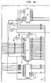
- FIG. 3 illustrates the circuitry for display unit 16.
- Unit 16 includes switch 30 coupled to the four low order bits (lines) of data bus 34 by buffers 38, 40, 42 and 44.
- the presently preferred embodiment of memory 36 may include a set for four jumpers 46, 48, 50 and 52. Jumpers 46, 48, 50 and 52 are coupled to the four high order bits (lines) of data bus 34 by buffers 54, 56, 58 and 60, respectively.
- address select line 62 of bus 34 (address 2A00 hex) goes low, switch 30 and memory 36 settings are read by processor 20 over data bus 34.
- Display unit 16 also includes four seven segment LED's 64, 66, 68 and 70, and a display driver 72.
- Data bus 80 couples display driver 72 to displays 64, 66, 68 and 70.
- Display driver 72 is coupled to data bus 34 and is controlled by address select lines 74 (address 2800 hex) and 76 (address 2900 hex).
- a data line 78 is the processor 20 read/write line. When processor 20 writes to address 2800, lines 74 and 78 go low. Address 2800 is used to send data to display driver 72. When processor 20 writes to address 2900, lines 76 and 78 go low. This address is used to sent control commands to display driver 72.
- data line J8-19, J8-17, J8-15, J8-13, J8-2, J8-4, J8-6, and J8-8 (DO-D7) connect unit 16 to trip unit 14 via data lines J2-19, J2-17, J2-15, J2-13, J2-2, J2-4, J2-6, and J2-8 (DO-D7), respectively.
- address select lines 74, 76, 62, and 78 are connected to trip unit 14 via address select lines J2-16, J2-14, J2-12 and the read/write line J2-10, respectively.
- the trip unit's processor/interface logic 15 includes a processor 20 (Motorola 68HC11F1) coupled to data bus 34, and buffer 82 also coupled to data bus 34. Buffer 82 acts as an isolation buffer between display unit 16 and trip unit 14 for data lines DO-D7.
- the processor/interface logic 15 of unit 14 also includes art isolation buffer 84 coupled to a decoder 86 which in turn is coupled to an address bus 88 coupled to processor 20. Buffer 84 acts as an isolation buffer between display unit 16 and trip unit 14 address select and read/write lines.
- the processor/interace logic 15 of trip unit 14 includes an EPROM 90 coupled to data bus 34 and address bus 88.
- the programming for processor 20, which controls the transfer of data between display unit 16 and trip unit 14, is stored in the memory of processor 20 and EPROM 90.
- processor 20 In operation, when processor 20 reads address 2AOO (address line 62), data bits 4 through 7, (data lines J8-2, J8-4, J8-6 and J8-8) are tested for a high state. If they do not all test high, then processor 20 assumes that trip unit 14 and display unit 16 are connected via connectors 26 and 32. In response, a portion of the display module control code is activated. Subsequently, the type of display unit 16 is determined by decoding data lines J8-8, J8-6, J8-4 and J8-2. After the type of display unit 16 is determined, the position of switch 30 is determined by decoding data lines J-8-13, J8-15, J8-17, and J8-19. Based upon this data, processor 20 then selects the function from the display module software (code) which is to be activated such that data is applied to display 28 to provide proper alphanumeric information at the display.
- display module software code
- processor 20 When the values displayed at display 28 are to be flashed due to a maximum phase current exceeding a set point, as discussed above, processor 20 alternately ends a display data command and a display blanking command to the display driver 72, thus causing the display 28 to flash.
- ground fault monitor module An example of a particularly useful type of display unit 16 is a ground fault monitor module.
- the internal circuitry of the ground fault module is identical to that of the general display unit of Figure 3.
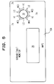
- the display unit 16 is configured as a ground fault monitor module by setting the jumpers 46-52 to a predetermined configuration (one that is recognized by the trip unit is being indicative of a ground fault monitor module) and by providing the module 16 with an appropriate face plate for indicating the functions associated with each of the positions of the rotary switch 30.
- a ground fault monitor module 16A The externals of such a ground fault monitor module 16A are shown Figures 5.
- the program code in the trip unit's EPROM 90 recognizes the jumper configuration as indicating that the display module 16 is a ground fault monitor module 16A.
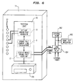
- the processor/interface logic 15 includes program code (executed by the processor 20) for performing ground fault level calculations 9.
- the processing/interface logic also includes code for a ground fault protection algorithm 17 (for the display module 16A) and can include program code for performing a separate and independent trip unit ground fault protection algorithm 11.
- Rotary switches 24 set the ground fault pickup and delay.
- the trip unit 14 includes an internal switch (not shown) the setting of which determines the ground fault calculation method. This switch is readable by the microprocessor 20. If the ground fault monitor module 16A is installed in a trip unit with a ground fault protection, the round fault type switch setting on the trip unit determines the calculation method (residual or source ground). In a non-ground fault trip unit, the ground fault type switch is set to the residual setting. If the module 16A is installed in a trip unit that does not include ground fault protection, the display module ground fault algorithm uses the residual current calculation method. The pickup and delay settings of the ground fault monitor module 16A work independently of the trip unit's internal ground fault pickup and delay settings set by the rotary switches 24.
- the ground fault pickup within the trip unit is divided into three levels; "Lo”, which is defined as 20 percent of the frame rating; "Hi”, which is defined as the frame rating or 1200 amps, whichever is less; and “Med”, which is defined as the average of the "Lo” and "Hi”.
- the ground fault trip delay is divided into three fixed times. These times are .1, .3 and .5 seconds.
- An additional monitoring option has a 1200 amp pickup and a .5 second delay.
- the rotary switch 30 of the ground fault monitor module 16A has ten positions.
- the switch 30 is read by the program code in the EPROM 90 to determine the user selected pickup and delay options.
- the user selects a Lo, Med or Hi pickup level, by way of the rotary switch 30, when selecting a time delay.
- the tenth position (MAX) indicates that the user has selected the 1200 amp pickup and a .5 second delay.
- the alarm line (LMA) is set to its "ON” state and remains in that state as long as the current is above the selected pickup.
- the alarm line is also set to its "ON” state if no module is installed or a module 16 is removed after the trip unit is powered up. Preferably, there is a delay before the alarm line is set to its "ON" state.
- the ground fault monitor 16A displays the ground fault current in amps when there is enough power to drive the display LEDs (3 phase - 8% frame rating, 2 phase - 12% frame rating, 1 phase 24% frame rating). When the ground fault current reaches a level 12 percent below the selected pickup, the amps displayed start to flash. This acts as an early warning alarm. When the ground fault current exceeds the selected ground fault pickup, the display will flash "OL".
- the ground fault monitor 16A can be used in conjunction with a local load monitor relay 604 to provide hard wired contacts for external ground fault protection 606 such as a shunt trip mechanism and/or an external alarm 602.
- the load monitor relay is driven by the alarm signal (LMA).
- FIG. 7 is a functional block diagram of the ground fault algorithms/mechanisms of Figure 6.
- the ground fault current level calculation algorithm 9 calculates the ground fault values based on either residual ground fault samples 704 or source ground fault samples 706 as directed by the setting of the ground fault type switch 708.
- the ground fault values calculated in block 702 are provided to the ground fault module algorithm (routines) 17 and the trip unit ground fault algorithm 11.
- the trip unit ground fault algorithm 11 compares the ground fault values with the settings of the trip unit ground fault pickup and delay rotary switches 24 and generates control signal on the trip line 712 when the ground fault values exceed the selected pickup setting for the selected delay time.
- the ground fault display module algorithm 17 In parallel with the activity of the trip unit ground fault algorithm 11, the ground fault display module algorithm 17 generates display data indicative of the ground fault values (and sends it to the module display 28) and compares the ground fault values to the pickup and delay settings of the rotary switch 30 of the ground fault display unit 16A. When the ground fault values exceed the thresholds set by the rotary switch 30 on the module 16A, the ground fault display module routines 17 generate a signal on the trip alarm line 716.
Landscapes
- Emergency Protection Circuit Devices (AREA)
- Breakers (AREA)
Description
- The present invention relates to a trip unit for a circuit breaker. More specifically, the present invention relates to a trip unit which is coupleable to one of a plurality of different display or monitor modules, where the trip unit is configured to automatically recognize the type of display or monitor module to which it is coupled and apply signals to the module which are compatible with the module.
- In general, display modules for circuit breaker trip units are known. Referring to U.S. Patent No. 4,870,531 issued to Robert J. Danek, there is shown a circuit interrupter having a display module for viewing circuit interrupter settings. The display module removably connects to the electronic trip unit of the interrupter by means of connectors, and displays interrupter values and settings when in operation. When the display module is not in place, a security cover may be positioned within a recess which is adapted to accept the display module. When the display module is in place, an operator actuates keys provided on the display module to select, through a process of the trip unit, the data to be displayed on the display module. Thus the prior art disclosed in U.S. Patent No. 4,870,531 corresponds to the preamble of
claim 1. - U.S. Patent No. 4,751,605, issued to Mertz et al., also discloses a trip unit for a circuit interrupter having a display module. The display module is portable and is coupleable to the trip unit to display various circuit interrupter values. The display module includes an alphanumeric display, a microprocessor, memory, and an apparatus associable with complementary apparatus in the trip unit to transfer the contents of memory areas in the trip unit to the memory of the display module. The content of the memory is selectively displayed by actuating keys provided on the display module.
- While various display module configurations are available for circuit interrupters (breakers), it would be useful and desirable to provide a trip unit useable with a plurality of different display modules, where each display module is configured to display a range of values for a given variable monitored by the trip unit e.g. current, temperature, energy, power, etc. Accordingly, depending upon the application for a circuit breaker, only a display module configured to display the variables which are needed for the application is provided.
- The present invention provides a trip unit as specified in
claim 1. The trip unit includes a first connector, a processor; a data bus coupled between the first connector and the processor; and a display or monitor module. The module includes a memory which stores configuration data that identifies the module and a second connector coupled to the memory and connected to the first connector of the trip unit. - The processor reads the configuration data, accesses a respective portion of program code based upon the configuration data read from the module, and transfers data between the processor and the module based upon the configuration data.
-
- Figure 1 is an exploded, schematic view of a circuit breaker contact and operating mechanism unit, a trip unit and a display module;
- Figure 2 is a side, schematic view of the circuit breaker contact and operating mechanism, trip unit and display module when coupled;
- Figure 3, which includes Figures 3A and 3B, is the circuit diagram for the display module;
- Figure 4, which includes Figures 4A, 4B, 4C and 4D, is the circuit diagram for the circuitry of the trip unit which interfaces with the display module;
- Figure. 5 is a block diagram of a ground fault display module according to an embodiment of the present invention;
- Figure 6 is a block diagram of a trip unit having a ground fault display module connected to an external load monitor relay according to an embodiment of the present invention; and,
- Figure 7 is a functional block diagram of the ground fault algorithms/mechanisms of Figure 6.
-
- Referring to Figures 1 and 2, a
circuit breaker 10 includes a circuit breaker contact andoperating mechanism 12, anelectronic trip unit 14, and a removable and interchangeable display unit ormodule 16.Mechanism 12 may be a conventional mechanism including the operating linkages and energy storing devices for opening the contacts ofcircuit breaker 10. Additionally,mechanism 12 includes monitoring devices, such as current transformers and temperature sensors, which produce status signals representative of the current flows and various temperatures incircuit breaker 10. The monitoring devices are electrically coupled to aconnector 18 of thetrip unit 14 such that the status signals for the monitoring devices are applied toconnector 18. Additionally,mechanism 12 includes tripping devices which are coupled toconnector 18 and causemechanism 12 to open the circuit breaker contacts in response to the application of control signals atconnector 18. -
Electronic trip unit 14 is of the type including a programmed micro-controller 20 (processor) which has circuitry coupled to aconnector 22 for monitoring the status signals applied toconnector 18. The circuitry includes devices for performing conditioning functions such as analog-to-digital conversion and filtering so thatprocessor 20 may properly monitor and analyze the status signals atconnector 18.Unit 14 also includes a plurality of limit set inputs such as rotary switches orpotentiometers 24.Rotary switches 24 allow variables such as long time delay, short time pick-up, short time delay, instantaneous pickup, ground fault pickup and ground fault delay to be adjusted. Based upon the values of the status signals and the settings atrotary switches 24,processor 20 applies the appropriate control signals and display signals toconnectors Connector 26 is connected toprocessor 20 by adata bus 34 and appropriate interface circuitry. -
Connector 22 is mechanically and electrically connected toconnector 18 whencircuit breaker 10 is assembled. - Display unit (module) 16 may have a plurality of configurations, and, generally, includes a
multi-digit display 28, amulti-position switch 30, aconnector 32, and amemory 36 for storing configuration data (address).Memory 36 may take the form of dip switches, a set of jumpers (presently preferred embodiment), PROM or other types of ROM.Display 28,switch 30 andmemory 36 are coupled toconnector 32 such that data may be transferred betweenunit 14 andunits 16 alongdata bus 34 whenunits connectors - When
unit 14 is operating, and coupled tounit 16,unit 14 reads the data in memory 36 (e.g. 4 bits, one associated with each of 4jumpers unit 16. All of the 4 bits of data are available for configuration data, thusunit 14 can automatically recognize up to 15 configurations ofdisplay unit 16. A 16th jumper/data configuration (all 4 data bits high) is recognized by thetrip unit 14 as indicating that adisplay unit 16 is not present. Upon recognizing theunit 16 configuration,processor 20 operates under the control of the portion of the program stored inunit 14 associated with the particular configuration. For example, oneunit 16 may be programmed to display amperage, where eachswitch 30 setting is associated with different amperage readings while other units may be configured to display a circuit breaker variable such as temperature, power or energy use. Furthermore,display unit 16 may be configured such thattrip unit 14 readsswitch 30 to acquire control or limit values such as alarm limits. By way of example,switch 30 may include 10 settings thus allowing the display of 10 different characteristics (values) of a given variable, control value or limit value. - Referring more specifically to the characteristics (values) associated with the ten switch positions of
switch 30, whenswitch 30 is associated with adisplay unit 16 configured to display amperage, switch 30 settings may include: - Present demand, which provides data for
processor 20 so that the average amperage load for the last 15 minute period is displayed; - Maximum demand, which provides data for
processor 20 so that the maximum amperage load since power was applied to the circuit breaker is displayed; - Phase A current, which provides data for
processor 20 so that the amperage load for phase A is displayed; - Phase B current, which provides data for
processor 20 so that the amperage load for phase B is displayed; - Phase C current, which provides data for
processor 20 so that the amperage load for phase C is displayed; - 60% load monitor set point, which provides data for
processor 20 so that the maximum phase current is displayed and flashed when the current exceeds 60% of the rated value; - 70% load monitor set point, which provides data for
processor 20 so that the maximum phase current is displayed and flashed when the current exceeds 70% of the rated value; - 80% load monitor set point, which provides data for
processor 20 so that the maximum phase current is displayed and flashed when the current exceeds 80% of the rated value; - 90% load monitor set point, which provides data for
processor 20 so that the maximum phase current is displayed and flashed when the current exceeds 90% of the rated value; and - 100% load monitor set point, which provides data for
processor 20 so that the maximum phase current is displayed and flashed when the current exceeds 100% of the rated value. -
- Subsequent to determining the configuration of a
particular display unit 16,processor 20 reads the status ofswitch 30, and transmits display data tounit 16 overdata bus 34, where the display data is representative of the characteristic selected atswitch 30 and the particular configuration of unit 16 (i.e. the data in memory 36). Thus, ifprocessor 20 readsmemory 36 and determines thatunit 16 is an amperage display unit, readsswitch 30 and determines that the RMS current for phase A is to be displayed,processor 20 will access the appropriate programming and apply the appropriate display data to display 28 viadata bus 34 to display the RMS current value for phase A in digital form (alphanumeric) ondisplay 28. - Referring to Figure 3, Figure 3 illustrates the circuitry for
display unit 16.Unit 16 includesswitch 30 coupled to the four low order bits (lines) ofdata bus 34 bybuffers memory 36 may include a set for fourjumpers Jumpers data bus 34 bybuffers select line 62 of bus 34 (address 2A00 hex) goes low,switch 30 andmemory 36 settings are read byprocessor 20 overdata bus 34. -
Display unit 16 also includes four seven segment LED's 64, 66, 68 and 70, and adisplay driver 72. (By way of modification, displays 64, 66, 68 and 70, anddisplay driver 72 may be replaced by a single chip unit depending upon the application.)Data bus 80 couples displaydriver 72 todisplays Display driver 72 is coupled todata bus 34 and is controlled by address select lines 74 (address 2800 hex) and 76 (address 2900 hex). Adata line 78 is theprocessor 20 read/write line. Whenprocessor 20 writes to address 2800,lines Address 2800 is used to send data to displaydriver 72. Whenprocessor 20 writes to address 2900,lines driver 72. - When
display unit 16 is plugged intotrip unit 14, data line J8-19, J8-17, J8-15, J8-13, J8-2, J8-4, J8-6, and J8-8 (DO-D7)connect unit 16 totrip unit 14 via data lines J2-19, J2-17, J2-15, J2-13, J2-2, J2-4, J2-6, and J2-8 (DO-D7), respectively. Also, addressselect lines unit 14 via address select lines J2-16, J2-14, J2-12 and the read/write line J2-10, respectively. - Referring to Figure 4, the trip unit's processor/
interface logic 15 includes a processor 20 (Motorola 68HC11F1) coupled todata bus 34, and buffer 82 also coupled todata bus 34.Buffer 82 acts as an isolation buffer betweendisplay unit 16 andtrip unit 14 for data lines DO-D7. The processor/interface logic 15 ofunit 14 also includesart isolation buffer 84 coupled to adecoder 86 which in turn is coupled to anaddress bus 88 coupled toprocessor 20.Buffer 84 acts as an isolation buffer betweendisplay unit 16 andtrip unit 14 address select and read/write lines. - In addition to
processor 20,buffer 82,buffer 84 anddecoder 86, the processor/interace logic 15 oftrip unit 14 includes anEPROM 90 coupled todata bus 34 andaddress bus 88. The programming forprocessor 20, which controls the transfer of data betweendisplay unit 16 andtrip unit 14, is stored in the memory ofprocessor 20 andEPROM 90. - In operation, when
processor 20 reads address 2AOO (address line 62),data bits 4 through 7, (data lines J8-2, J8-4, J8-6 and J8-8) are tested for a high state. If they do not all test high, thenprocessor 20 assumes thattrip unit 14 anddisplay unit 16 are connected viaconnectors display unit 16 is determined by decoding data lines J8-8, J8-6, J8-4 and J8-2. After the type ofdisplay unit 16 is determined, the position ofswitch 30 is determined by decoding data lines J-8-13, J8-15, J8-17, and J8-19. Based upon this data,processor 20 then selects the function from the display module software (code) which is to be activated such that data is applied to display 28 to provide proper alphanumeric information at the display. - When the values displayed at
display 28 are to be flashed due to a maximum phase current exceeding a set point, as discussed above,processor 20 alternately ends a display data command and a display blanking command to thedisplay driver 72, thus causing thedisplay 28 to flash. - An example of a particularly useful type of
display unit 16 is a ground fault monitor module. Advantageously, the internal circuitry of the ground fault module is identical to that of the general display unit of Figure 3. - The
display unit 16 is configured as a ground fault monitor module by setting the jumpers 46-52 to a predetermined configuration (one that is recognized by the trip unit is being indicative of a ground fault monitor module) and by providing themodule 16 with an appropriate face plate for indicating the functions associated with each of the positions of therotary switch 30. The externals of such a groundfault monitor module 16A are shown Figures 5. - When the
ground fault module 16A is plugged into thetrip unit 14, the program code in the trip unit'sEPROM 90 recognizes the jumper configuration as indicating that thedisplay module 16 is a groundfault monitor module 16A. - As illustrated in Figure 6, the processor/
interface logic 15 includes program code (executed by the processor 20) for performing groundfault level calculations 9. The processing/interface logic also includes code for a ground fault protection algorithm 17 (for thedisplay module 16A) and can include program code for performing a separate and independent trip unit groundfault protection algorithm 11. Rotary switches 24 set the ground fault pickup and delay. When the trip unit groundfault protection algorithm 11 detects that the ground fault current has exceeded the pickup setting for the selected time delay, it takes appropriate action (e.g. causes a trip) in response thereto. - The
trip unit 14 includes an internal switch (not shown) the setting of which determines the ground fault calculation method. This switch is readable by themicroprocessor 20. If the groundfault monitor module 16A is installed in a trip unit with a ground fault protection, the round fault type switch setting on the trip unit determines the calculation method (residual or source ground). In a non-ground fault trip unit, the ground fault type switch is set to the residual setting. If themodule 16A is installed in a trip unit that does not include ground fault protection, the display module ground fault algorithm uses the residual current calculation method. The pickup and delay settings of the groundfault monitor module 16A work independently of the trip unit's internal ground fault pickup and delay settings set by the rotary switches 24. - The ground fault pickup within the trip unit is divided into three levels; "Lo", which is defined as 20 percent of the frame rating; "Hi", which is defined as the frame rating or 1200 amps, whichever is less; and "Med", which is defined as the average of the "Lo" and "Hi". The ground fault trip delay is divided into three fixed times. These times are .1, .3 and .5 seconds. An additional monitoring option has a 1200 amp pickup and a .5 second delay.
- Turning again to FIG. 5, the
rotary switch 30 of the groundfault monitor module 16A has ten positions. Theswitch 30 is read by the program code in theEPROM 90 to determine the user selected pickup and delay options. The user selects a Lo, Med or Hi pickup level, by way of therotary switch 30, when selecting a time delay. The tenth position (MAX) indicates that the user has selected the 1200 amp pickup and a .5 second delay. - When the ground fault exceeds the selected pickup and delay, the alarm line ("LMA") is set to its "ON" state and remains in that state as long as the current is above the selected pickup. The alarm line is also set to its "ON" state if no module is installed or a
module 16 is removed after the trip unit is powered up. Preferably, there is a delay before the alarm line is set to its "ON" state. - The
ground fault monitor 16A displays the ground fault current in amps when there is enough power to drive the display LEDs (3 phase - 8% frame rating, 2 phase - 12% frame rating, 1phase 24% frame rating). When the ground fault current reaches alevel 12 percent below the selected pickup, the amps displayed start to flash. This acts as an early warning alarm. When the ground fault current exceeds the selected ground fault pickup, the display will flash "OL". - As illustrated in FIG. 6, the
ground fault monitor 16A can be used in conjunction with a localload monitor relay 604 to provide hard wired contacts for externalground fault protection 606 such as a shunt trip mechanism and/or anexternal alarm 602. The load monitor relay is driven by the alarm signal (LMA). - Figure 7 is a functional block diagram of the ground fault algorithms/mechanisms of Figure 6. In
block 702, the ground fault currentlevel calculation algorithm 9 calculates the ground fault values based on either residualground fault samples 704 or sourceground fault samples 706 as directed by the setting of the groundfault type switch 708. The ground fault values calculated inblock 702 are provided to the ground fault module algorithm (routines) 17 and the trip unitground fault algorithm 11. The trip unitground fault algorithm 11 compares the ground fault values with the settings of the trip unit ground fault pickup and delay rotary switches 24 and generates control signal on thetrip line 712 when the ground fault values exceed the selected pickup setting for the selected delay time. In parallel with the activity of the trip unitground fault algorithm 11, the ground faultdisplay module algorithm 17 generates display data indicative of the ground fault values (and sends it to the module display 28) and compares the ground fault values to the pickup and delay settings of therotary switch 30 of the groundfault display unit 16A. When the ground fault values exceed the thresholds set by therotary switch 30 on themodule 16A, the ground faultdisplay module routines 17 generate a signal on thetrip alarm line 716. - It will be understood that the above description is of the preferred exemplary embodiment of the invention, and that the invention is not limited to the specific form shown. For example, various components of the above-described trip unit and display unit may be modified to combine various discreet components into single multi-function components. Furthermore, it is contemplated that portions of the software may be replaced with appropriately configured hardware, and, alternatively, depending upon the microprocessor or controller used as
processor 20, the software may be modified such that hardware in the circuits may be eliminated. Various other substitutions, modifications, changes and omissions may be made without departing from the scope of the invention, as defined in the appended claims.
Claims (16)
- A trip unit (14) comprising:a first connector (26);a processor (20);a data bus (34) coupled between the first connector (26) and the processor (20); anda display or monitor module (16, 16A) including a second connector (32) connected to said first connector (26);
characterised in that the display or monitor module (16, 16A) includes a memory (36) which stores configuration data that identifies the module (16, 16A), which memory (36) is coupled to said second connector (32);
wherein the processor (20) is arranged for reading the configuration data, accessing a respective portion of program code based upon the configuration data read from the memory (36) of the display or monitor module (16, 16A), and transferring data between the processor (20) and the display or monitor module (16, 16A) based upon the configuration data. - Trip unit according to Claim 1, characterized in that the trip unit (14) is arranged to operate a circuit breaker.
- Trip unit according to Claim 1 characterized in that the trip unit (14) is arranged to operate a ground fault circuit breaker and the display or monitor module is a ground fault monitor module (16A).
- Trip unit according to Claim 1, where the memory (36)is a set of jumpers (46-52).
- Trip unit according to Claim 3 where the ground fault monitor module(16A) comprises a digital display (28) which displays alphanumeric data in response to data transferred from the processor (20) to the module (16A).
- Trip unit according to Claim 5, where the ground fault monitor module (16A) comprises a switch (30) coupled to the second connector (32) to provide control data to the processor (20), the processor providing display data to the digital display (28) which is dependent upon the control data.
- Trip unit according to Claim 3, where the ground fault monitor module (16A) comprises a switch (30) coupled to the second connector (32) to provide control data to the processor (20), where the processor sets limit values in the trip unit (14) based upon the control data.
- Trip unit according to Claim 7, wherein the control data comprises pick-up and delay settings and wherein the trip unit comprises (14) means for generating a first alarm signal (714) when detected ground fault parameters exceed the pick-up and delay settings.
- Trip unit according to Claim 8, wherein the trip unit comprises an internal ground fault protection mechanism having an internal set of pickup and delay settings and wherein the means for generating the alarm signal (714) operates independent of the internal set of pickup and delay settings.
- Trip unit according to Claim 8, further comprising means for generating a second alarm signal responsive to ground fault parameters exceeding internal pickup and delay settings, wherein the second alarm signal is operable independently of the first alarm signal.
- Trip unit according to Claim 10, wherein the second alarm signal is connected to operate a shunt trip mechanism (606).
- Trip unit according to Claim 1, characterized in that the module (16A) comprises a plug-in ground fault monitor module having:means for mechanically seating the module in the trip unit;said memory (36) for storing the configuration data (36);a digital display (28) which displays alphanumeric data, in response to the data transferred from the processor (20) to the module; andsaid second connector (32) coupled to the memory means (36) for providing a data transfer path between the processor (20)and the module (16A) wherein the data transfer path provides the processor (20) with access to the configuration data and the digital display (28).
- The unit of Claim 12, where the memory (36) is a set of jumpers(46-52).
- The unit of Claim 12, where the ground fault monitor module (16A) comprises a switch (30) coupled to the connector (32) to provide control data to the processor (20).
- The unit of Claim 12, where the ground fault monitor module (16A) further comprises:a switch (30) coupled to the connector (32) to provide control data to the processor (20); anda visual indicator which indicates levels at which the trip unit will set limit values based upon the control data generated by a position of the switch.
- Trip unit according to Claim 1, characterized in that the module comprises a plug-in ground fault monitor module having:means for mechanically seating the module in the trip unit;at least one jumper (46-52) for storing the configuration data;a digital display (28) which displays alphanumeric data in response to the data transferred from the processor (20) to the module;said second connector (32) coupled to the memory (36) for providing a data transfer path between the processor (20)and the module (16A) wherein the data transfer path provides the processor (20) with access to the configuration data and the digital display (28);a user operable switch (30) coupled to the connector (32) to provide control data to the processor (20); anda visual indicator which indicates levels at which the trip unit will set limit values based upon the control data generated by a position of the switch.
Applications Claiming Priority (2)
| Application Number | Priority Date | Filing Date | Title |
|---|---|---|---|
| US14306 | 1993-02-05 | ||
| US08/014,306 US5490086A (en) | 1992-03-06 | 1993-02-05 | Plug-in ground fault monitor for a circuit breaker |
Publications (2)
| Publication Number | Publication Date |
|---|---|
| EP0609898A1 EP0609898A1 (en) | 1994-08-10 |
| EP0609898B1 true EP0609898B1 (en) | 2000-09-20 |
Family
ID=21764689
Family Applications (1)
| Application Number | Title | Priority Date | Filing Date |
|---|---|---|---|
| EP94101732A Expired - Lifetime EP0609898B1 (en) | 1993-02-05 | 1994-02-04 | Electronic trip unit having a display module |
Country Status (5)
| Country | Link |
|---|---|
| US (1) | US5490086A (en) |
| EP (1) | EP0609898B1 (en) |
| CA (1) | CA2114889C (en) |
| DE (1) | DE69425916T2 (en) |
| ES (1) | ES2152267T3 (en) |
Families Citing this family (38)
| Publication number | Priority date | Publication date | Assignee | Title |
|---|---|---|---|---|
| US5691897A (en) * | 1995-05-30 | 1997-11-25 | Roy-G-Biv Corporation | Motion control systems |
| US5706204A (en) * | 1996-02-28 | 1998-01-06 | Eaton Corporation | Apparatus for triggering alarms and waveform capture in an electric power system |
| US5706153A (en) * | 1996-06-03 | 1998-01-06 | Eaton Corporation | Programmer for starter |
| US5796636A (en) * | 1996-07-12 | 1998-08-18 | Andrews; Lowell B. | Apparatus for and method of testing an electrical ground fault circuit interrupt device |
| US5859596A (en) * | 1996-08-30 | 1999-01-12 | Csi Technology, Inc. | Switchyard equipment monitoring system and communications network therefor |
| US5877925A (en) * | 1996-12-17 | 1999-03-02 | General Electric Company | Ground fault-rating plug for molded case circuit breakers |
| FI965176A0 (en) * | 1996-12-20 | 1996-12-20 | James Nimmo | The programmer saws as well as the programming steps above |
| ES2163275T3 (en) * | 1997-03-27 | 2002-01-16 | Siemens Ag | COMMAND DEVICE FOR CONDUCTING SWITCHING OPERATIONS IN A SWITCHING INSTALLATION. |
| US6169651B1 (en) * | 1998-06-05 | 2001-01-02 | General Electric Company | Protective relay with modular control panel |
| US6018451A (en) * | 1998-09-28 | 2000-01-25 | Siemens Energy & Automation, Inc. | Circuit breaker trip unit and method for real-time fault indication |
| US6191947B1 (en) | 1998-09-28 | 2001-02-20 | Siemens Energy & Automation, Inc. | Electronic trip unit and mounting method |
| US6459370B1 (en) | 1998-11-03 | 2002-10-01 | Adt Services Ag | Method and apparatus for determining proper installation of alarm devices |
| US6121886A (en) * | 1999-05-18 | 2000-09-19 | General Electric Company | Method for predicting fault conditions in an intelligent electronic device |
| GB0120748D0 (en) | 2001-08-25 | 2001-10-17 | Lucas Aerospace Power Equip | Generator |
| US6678135B2 (en) * | 2001-09-12 | 2004-01-13 | General Electric Company | Module plug for an electronic trip unit |
| US6804101B2 (en) * | 2001-11-06 | 2004-10-12 | General Electric Company | Digital rating plug for electronic trip unit in circuit breakers |
| US6546342B1 (en) * | 2001-12-10 | 2003-04-08 | General Electric Company | Adaptive algorithm to prevent nuissance tripping |
| US7532955B2 (en) * | 2002-02-25 | 2009-05-12 | General Electric Company | Distributed protection system for power distribution systems |
| AU2003217663A1 (en) * | 2002-02-25 | 2003-09-09 | General Electric Company | Method and system for conditionally triggered system data capture |
| US7747356B2 (en) | 2002-02-25 | 2010-06-29 | General Electric Company | Integrated protection, monitoring, and control system |
| US7058482B2 (en) * | 2002-02-25 | 2006-06-06 | General Electric Company | Data sample and transmission modules for power distribution systems |
| US7111195B2 (en) * | 2002-02-25 | 2006-09-19 | General Electric Company | Method and system for external clock to obtain multiple synchronized redundant computers |
| US7636616B2 (en) * | 2003-02-25 | 2009-12-22 | General Electric Company | Protection system for power distribution systems |
| US7039822B2 (en) * | 2003-02-27 | 2006-05-02 | Promos Technologies Inc. | Integrated circuit memory architecture with selectively offset data and address delays to minimize skew and provide synchronization of signals at the input/output section |
| GB2401467B (en) * | 2003-05-09 | 2006-01-25 | Autoliv Dev | Improvements in or relating to a movable or removable unit for a motor vehicle |
| US20050047045A1 (en) * | 2003-08-29 | 2005-03-03 | Puskar Michael P. | Circuit breaker and trip unit employing multiple function time selector switch |
| US20080157776A1 (en) * | 2006-12-28 | 2008-07-03 | Adil Jaffer | Measurement of analog coil voltage and coil current |
| US20080158762A1 (en) * | 2006-12-29 | 2008-07-03 | Brian Patrick Lenhart | Circuit breaker trip unit rating selection plug |
| US7633399B2 (en) * | 2007-02-27 | 2009-12-15 | Eaton Corporation | Configurable arc fault or ground fault circuit interrupter and method |
| PL2079091T3 (en) | 2008-01-10 | 2014-07-31 | Schneider Electric Ind Sas | Voltage trigger case for a circuit breaker, voltage trigger device and assembly method |
| US20090195337A1 (en) * | 2008-01-31 | 2009-08-06 | Carlino Harry J | Manually selectable instantaneous current settings for a trip unit and electrical switching apparatus including the same |
| US20110087383A1 (en) * | 2009-10-08 | 2011-04-14 | Eaton Corporation | Network protection with control health monitoring |
| DE102011085601A1 (en) * | 2011-11-02 | 2013-05-02 | Siemens Aktiengesellschaft | Trigger unit for triggering a triggering element of an electrical switching device and electrical switching device |
| US9054513B2 (en) | 2012-10-17 | 2015-06-09 | General Electric Company | Circuit protection device and methods of configuring a circuit protection device |
| US9991693B2 (en) | 2012-10-17 | 2018-06-05 | General Electric Company | Circuit protection device and methods of configuring a circuit protection device |
| DE102014201501A1 (en) | 2014-01-28 | 2015-07-30 | Siemens Aktiengesellschaft | External control of an electromagnetic release |
| DE102015210937A1 (en) * | 2015-06-15 | 2016-12-15 | Tridonic Gmbh & Co Kg | Building services equipment with display module |
| US20230291206A1 (en) * | 2022-03-14 | 2023-09-14 | Eflex, Inc. | Energy management system and method |
Family Cites Families (39)
| Publication number | Priority date | Publication date | Assignee | Title |
|---|---|---|---|---|
| DE193732C (en) * | 1906-01-26 | |||
| FR493272A (en) * | 1918-11-23 | 1919-08-05 | Henri Adrien Mortier | Hand washing apparatus, particularly suitable for people deprived of the use of one hand |
| US4143417A (en) * | 1976-10-21 | 1979-03-06 | The Singer Company | Portable data-gathering apparatus formed by modular components having operate-standby modes |
| US4245318A (en) * | 1979-05-07 | 1981-01-13 | General Electric Company | Circuit breaker demonstrator and distribution circuit protection coordinator apparatus |
| US4351012A (en) * | 1980-04-15 | 1982-09-21 | Westinghouse Electric Corp. | Circuit interrupter with digital trip unit and means to enter trip settings |
| US4377837A (en) * | 1980-04-15 | 1983-03-22 | Westinghouse Electric Corp. | Circuit interrupter with overtemperature trip device |
| US4377836A (en) * | 1980-04-15 | 1983-03-22 | Westinghouse Electric Corp. | Circuit interrupter with solid state digital trip unit and positive power-up feature |
| US4431988A (en) * | 1981-01-23 | 1984-02-14 | Bristol Babcock Inc. | Microprocessor-based keyboard/display unit for configuring control instruments |
| DE3104535C2 (en) * | 1981-02-09 | 1986-07-03 | Dieter Gräßlin Feinwerktechnik, 7742 St Georgen | Time switch |
| US4467434A (en) * | 1981-09-18 | 1984-08-21 | Mcgraw-Edison Co. | Solid state watt-hour meter |
| US4535409A (en) * | 1981-09-18 | 1985-08-13 | Mcgraw-Edison Company | Microprocessor based recloser control |
| US4527285A (en) * | 1982-03-29 | 1985-07-02 | International Business Machines Corporation | Pluggable terminal architecture |
| US4481512A (en) * | 1982-12-29 | 1984-11-06 | Audio Systems, Inc. | Theft-resistant audio system for vehicle |
| US4628397A (en) * | 1984-06-04 | 1986-12-09 | General Electric Co. | Protected input/output circuitry for a programmable controller |
| US4672501A (en) * | 1984-06-29 | 1987-06-09 | General Electric Company | Circuit breaker and protective relay unit |
| US4589052A (en) * | 1984-07-17 | 1986-05-13 | General Electric Company | Digital I2 T pickup, time bands and timing control circuits for static trip circuit breakers |
| US4631625A (en) * | 1984-09-27 | 1986-12-23 | Siemens Energy & Automation, Inc. | Microprocessor controlled circuit breaker trip unit |
| FR2578113B1 (en) * | 1985-02-25 | 1988-04-15 | Merlin Gerin | DIGITAL STATIC TRIGGER WITH OPTIONAL FUNCTIONS FOR AN ELECTRIC CIRCUIT BREAKER |
| FR2592737B1 (en) * | 1986-01-03 | 1988-03-18 | Merlin Gerin | READER FOR A DIGITAL TRIGGER ASSOCIATED WITH A POWER CUT-OFF APPARATUS |
| AU594385B2 (en) * | 1986-03-20 | 1990-03-08 | Wang Laboratories, Inc. | Display attachment apparatus |
| FR2602610B1 (en) * | 1986-08-08 | 1994-05-20 | Merlin Et Gerin | STATIC TRIGGER OF AN ELECTRIC CIRCUIT BREAKER WITH CONTACT WEAR INDICATOR |
| US4897756A (en) * | 1987-01-30 | 1990-01-30 | Square D Company | Add-on ground fault module |
| US4794484A (en) * | 1987-02-20 | 1988-12-27 | Westinghouse Electric Corp. | Circuit interrupter apparatus with a style saving override circuit |
| US4752853A (en) * | 1987-02-20 | 1988-06-21 | Westinghouse Electric Corp. | Circuit interrupter apparatus with an integral trip curve display |
| US4827369A (en) * | 1987-02-20 | 1989-05-02 | Westinghouse Electric Corp. | Circuit interrupter apparatus with a selectable display means |
| US4728914A (en) * | 1987-05-04 | 1988-03-01 | General Electric Company | Rating plug enclosure for molded case circuit breakers |
| US4814712A (en) * | 1987-06-17 | 1989-03-21 | General Electric Company | Test kit for a circuit breaker containing an electronic trip unit |
| US4794356A (en) * | 1987-12-16 | 1988-12-27 | General Electric Company | Molded case circuit breaker auxiliary switch unit |
| US5166887A (en) * | 1988-03-31 | 1992-11-24 | Square D Company | Microcomputer-controlled circuit breaker system |
| US4870531A (en) * | 1988-08-15 | 1989-09-26 | General Electric Company | Circuit breaker with removable display and keypad |
| US4991105A (en) * | 1988-12-21 | 1991-02-05 | Accu-Scan, Inc. | Microprocessor controlled ground system monitor |
| US4979070A (en) * | 1989-06-13 | 1990-12-18 | Bodkin Lawrence E | Automatic reset circuit for GFCI |
| US5136457A (en) * | 1989-08-31 | 1992-08-04 | Square D Company | Processor controlled circuit breaker trip system having an intelligent rating plug |
| US4945443A (en) * | 1989-09-14 | 1990-07-31 | General Electric Company | Electronic circuit interrupter with combined keypad and display |
| US5051861A (en) * | 1990-01-09 | 1991-09-24 | General Electric Company | Multiple circuit interrupter address identification system |
| US4958252A (en) * | 1990-01-16 | 1990-09-18 | Westinghouse Electric Corp. | Circuit breaker with rating plug having memory |
| JP3151490B2 (en) * | 1990-07-13 | 2001-04-03 | 松下電工株式会社 | Setting method of ID code in wireless transmitter |
| US5204798A (en) * | 1991-07-22 | 1993-04-20 | General Electric Company | Metering accessory for molded case circuit breakers |
| US5311392A (en) * | 1991-08-30 | 1994-05-10 | Siemens Energy & Automation, Inc. | Dual processor electric power trip unit |
-
1993
- 1993-02-05 US US08/014,306 patent/US5490086A/en not_active Expired - Fee Related
-
1994
- 1994-02-03 CA CA002114889A patent/CA2114889C/en not_active Expired - Fee Related
- 1994-02-04 ES ES94101732T patent/ES2152267T3/en not_active Expired - Lifetime
- 1994-02-04 EP EP94101732A patent/EP0609898B1/en not_active Expired - Lifetime
- 1994-02-04 DE DE69425916T patent/DE69425916T2/en not_active Expired - Fee Related
Also Published As
| Publication number | Publication date |
|---|---|
| DE69425916D1 (en) | 2000-10-26 |
| EP0609898A1 (en) | 1994-08-10 |
| ES2152267T3 (en) | 2001-02-01 |
| CA2114889A1 (en) | 1994-08-06 |
| CA2114889C (en) | 1999-08-31 |
| US5490086A (en) | 1996-02-06 |
| DE69425916T2 (en) | 2001-03-29 |
Similar Documents
| Publication | Publication Date | Title |
|---|---|---|
| US5490086A (en) | Plug-in ground fault monitor for a circuit breaker | |
| CA2150198C (en) | Digitally controlled circuit interrupter with improved automatic selection of sampling interval for 50 hz and 60 hz power systems | |
| US5220479A (en) | Electronic trip device whose front panel is formed by a flat screen display | |
| US4428022A (en) | Circuit interrupter with digital trip unit and automatic reset | |
| US6678135B2 (en) | Module plug for an electronic trip unit | |
| US4331999A (en) | Circuit interrupter with digital trip unit and power supply | |
| US4351012A (en) | Circuit interrupter with digital trip unit and means to enter trip settings | |
| US4377837A (en) | Circuit interrupter with overtemperature trip device | |
| US4331998A (en) | Circuit interrupter with digital trip unit and style designator circuit | |
| US4331997A (en) | Circuit interrupter with digital trip unit and potentiometers for parameter entry | |
| EP0957556A2 (en) | Electrical switching device or trip unit acquiring predetermined settings from another electrical switching device or trip unit | |
| US5699222A (en) | Apparatus and method for programming and reviewing a plurality of parameters of electrical switching device | |
| US20030193767A1 (en) | Electronic trip unit capable of analog and digital setting of circuit breaker setpoints | |
| US6246928B1 (en) | Electrical interruption device comprising a communication module | |
| US4670812A (en) | System for monitoring the operating condition of a switch to prevent overstress | |
| US6836396B1 (en) | World wide web enabled and digital rating plug | |
| AU749406B2 (en) | Electrical switching apparatus employing interlocks for first and second trip functions | |
| US5426592A (en) | Circuit breaker trip unit which automatically adapts to operated with a particular display module | |
| CN1589516A (en) | Control and protection module of a switch device | |
| EP1101155A1 (en) | An intelligent electronic device for monitoring non-electrical characteristics | |
| US5331501A (en) | Electrical switching apparatus with digital trip unit and memory reset | |
| CA2145471C (en) | Overcurrent trip unit with separately adjustable neutral protection | |
| US20020183871A1 (en) | Hand-held device for a programmable control unit | |
| EP0333412B1 (en) | Circuit breakers test device | |
| EP0774821A2 (en) | Test circuit for electrical switching device |
Legal Events
| Date | Code | Title | Description |
|---|---|---|---|
| PUAI | Public reference made under article 153(3) epc to a published international application that has entered the european phase |
Free format text: ORIGINAL CODE: 0009012 |
|
| AK | Designated contracting states |
Kind code of ref document: A1 Designated state(s): DE ES FR GB IT |
|
| 17P | Request for examination filed |
Effective date: 19950208 |
|
| 17Q | First examination report despatched |
Effective date: 19980317 |
|
| GRAG | Despatch of communication of intention to grant |
Free format text: ORIGINAL CODE: EPIDOS AGRA |
|
| RTI1 | Title (correction) |
Free format text: ELECTRONIC TRIP UNIT HAVING A DISPLAY MODULE |
|
| GRAG | Despatch of communication of intention to grant |
Free format text: ORIGINAL CODE: EPIDOS AGRA |
|
| GRAH | Despatch of communication of intention to grant a patent |
Free format text: ORIGINAL CODE: EPIDOS IGRA |
|
| GRAH | Despatch of communication of intention to grant a patent |
Free format text: ORIGINAL CODE: EPIDOS IGRA |
|
| GRAA | (expected) grant |
Free format text: ORIGINAL CODE: 0009210 |
|
| AK | Designated contracting states |
Kind code of ref document: B1 Designated state(s): DE ES FR GB IT |
|
| REF | Corresponds to: |
Ref document number: 69425916 Country of ref document: DE Date of ref document: 20001026 |
|
| ITF | It: translation for a ep patent filed | ||
| ET | Fr: translation filed | ||
| REG | Reference to a national code |
Ref country code: ES Ref legal event code: FG2A Ref document number: 2152267 Country of ref document: ES Kind code of ref document: T3 |
|
| PLBE | No opposition filed within time limit |
Free format text: ORIGINAL CODE: 0009261 |
|
| STAA | Information on the status of an ep patent application or granted ep patent |
Free format text: STATUS: NO OPPOSITION FILED WITHIN TIME LIMIT |
|
| 26N | No opposition filed | ||
| REG | Reference to a national code |
Ref country code: GB Ref legal event code: IF02 |
|
| PGFP | Annual fee paid to national office [announced via postgrant information from national office to epo] |
Ref country code: GB Payment date: 20040205 Year of fee payment: 11 |
|
| PGFP | Annual fee paid to national office [announced via postgrant information from national office to epo] |
Ref country code: ES Payment date: 20040213 Year of fee payment: 11 |
|
| PGFP | Annual fee paid to national office [announced via postgrant information from national office to epo] |
Ref country code: FR Payment date: 20040226 Year of fee payment: 11 |
|
| PGFP | Annual fee paid to national office [announced via postgrant information from national office to epo] |
Ref country code: DE Payment date: 20040419 Year of fee payment: 11 |
|
| PG25 | Lapsed in a contracting state [announced via postgrant information from national office to epo] |
Ref country code: IT Free format text: LAPSE BECAUSE OF NON-PAYMENT OF DUE FEES;WARNING: LAPSES OF ITALIAN PATENTS WITH EFFECTIVE DATE BEFORE 2007 MAY HAVE OCCURRED AT ANY TIME BEFORE 2007. THE CORRECT EFFECTIVE DATE MAY BE DIFFERENT FROM THE ONE RECORDED. Effective date: 20050204 Ref country code: GB Free format text: LAPSE BECAUSE OF NON-PAYMENT OF DUE FEES Effective date: 20050204 |
|
| PG25 | Lapsed in a contracting state [announced via postgrant information from national office to epo] |
Ref country code: ES Free format text: LAPSE BECAUSE OF NON-PAYMENT OF DUE FEES Effective date: 20050205 |
|
| PG25 | Lapsed in a contracting state [announced via postgrant information from national office to epo] |
Ref country code: DE Free format text: LAPSE BECAUSE OF NON-PAYMENT OF DUE FEES Effective date: 20050901 |
|
| GBPC | Gb: european patent ceased through non-payment of renewal fee |
Effective date: 20050204 |
|
| PG25 | Lapsed in a contracting state [announced via postgrant information from national office to epo] |
Ref country code: FR Free format text: LAPSE BECAUSE OF NON-PAYMENT OF DUE FEES Effective date: 20051031 |
|
| REG | Reference to a national code |
Ref country code: FR Ref legal event code: ST Effective date: 20051031 |
|
| REG | Reference to a national code |
Ref country code: ES Ref legal event code: FD2A Effective date: 20050205 |